

Pioneer DVR-225-S, DVR-225 Service manual
Training Guide
DVR-65H-S / DVR-520H-S
DVR-320-S / DVR-225-S
DVR-220-S
Technical Training Department
1925 East Dominguez Street
Long Beach, CA 90810


Contents
Overview
Block Diagrams
Recording Block 6~7 Service Modes 29~51
Preview Block 8~9 Service Mode Screens 29~35
Overall Board Layout 10 Error Codes 36~39
Main Board 11~12 Key Codes 40~42
HDD Unit 13 Simple DV Diagnosis 43
Overall Block Diagrams 14~17 Error Rate Measurements 44~45
System Configuration 15 Channel Setting Mode 46~49
Complete Block 16~17 Aging Modes 50~51
Adjustments & Data Setting Modes 18~52 Start-Up Sequence 52
4 Model Number Setting 26
5~9 Disc Download Procedure 27~28
Tuner & Main PCB Adjustments 19~20 Disassembly Section 53~58
Service Diagnosis List 21 LSI_NG & Flash_NG Diagnosis 60~66
CPRM ID Number & Data Setting 22~25 HDD Diagnosis Method 68~74

Overview
4
All five models covered in this guide have the same basic construction, board layout
and electronic circuit design. Block diagrams shown will be of the DVR-520H-S and
DVR-65H-S. The adjustment and test mode sections will be the same for all models
with the exception of additional test modes for the hard drive models.
Basic differences in models from the DVR-520H-S & DVR-65H-S are as follows:
• DVR-320-S………..No hard drive.
• DVR-225-S & DVR-220-S………..No hard drive or DV in/out terminal.
All models listed use the (R-7) DVDR/RW writer drive

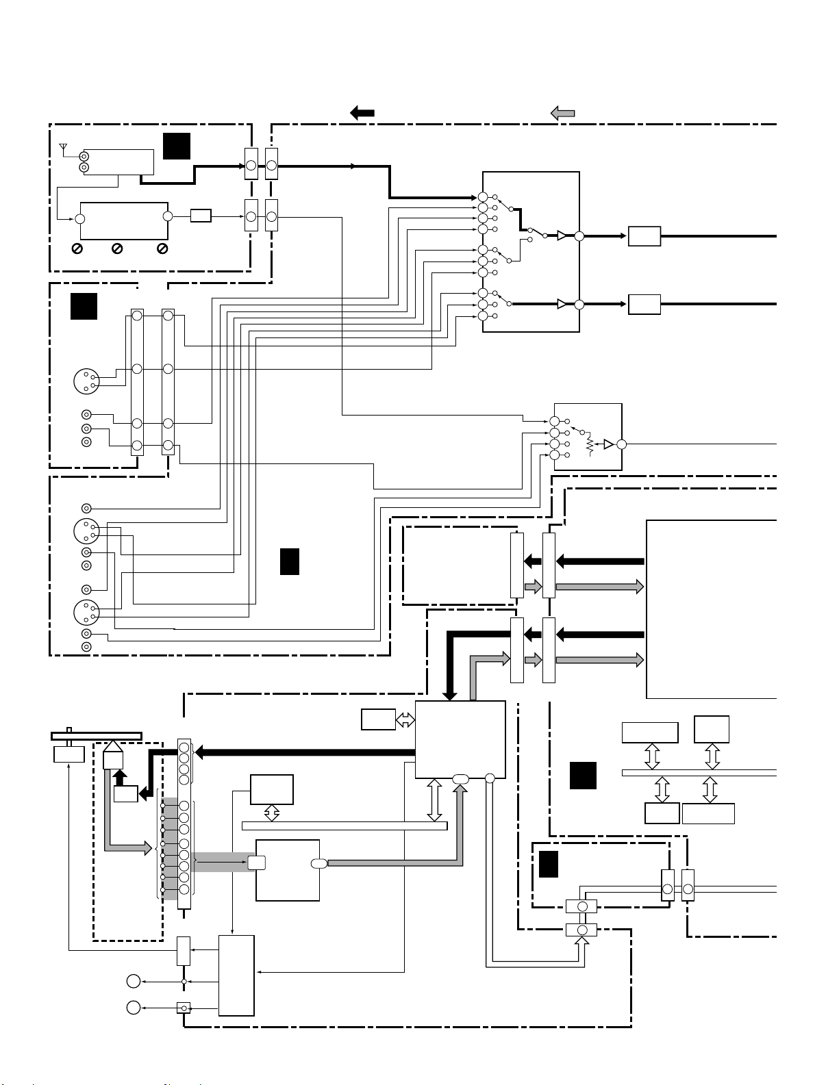
Block Diagrams
Tuner & Line Input Recording
6
SIGNAL FLOW
DVD-R/RW Drive
Hard Disk Drive
ATA
SDRAM
Frame
AV-Enc.
ATA I/F
256Mb
TBC
ENC
128Mb
SDRAM
3D Y/C
DNR
(REC)
AV-codec
LSI
M65672WG
DEC
64Mb
SDRAM
1394 Link
DV-codec
Video
ADC
PAL/NTSC
Decoder
32bit RISC
CPU
1394
Phy.
SRC
Audio
A/D
S
1
F
B
S
Stereo
Video
Input
Selector
Audio
U
P
C
D
R
A
M
M
8
2
b
A
S
L
H
M
b
4
6
k
c
a
p
u
A
R
M
M
b
4
Decoder
Tuner/FL
Control CPU
TV
Tuner
Line-In
Select
INPUT
OUTPUT
AV-Dec.
Graphics
Engine
3D DNR
(PB)
Progressive
Converter
Video
DAC
PAL/NTSC
Encoder
Audio
D/A
Y/C/CVBS Video Out
Y/Cb/Cr Video Out
Audio Analog Out
DIF Out (Opt.)

Signal flow Record Mode
7
All video and audio record signals from tuner assembly, composite or S inputs pass
through the jack panel assembly with the exception of the DV input/output.
The Tuner/FL Control CPU instructs an input selector based on user settings and
sends the audio and video analog signals to the AV-codec IC .
This AV-codec IC will take the analog audio and video input signals convert them
to a digital DVD format and interface with the DVD-R/RW drive or the Hard Disk
for recording.
In normal recording mode the video output signal from the AV-codec IC is basically
a direct loop through the processing IC.
DV input/output record and playback line enter the AV-codec IC from the DV jack
assembly. An audio sampling rate converter (SRC) is used to convert all incoming
DV audio to 48kh
z.
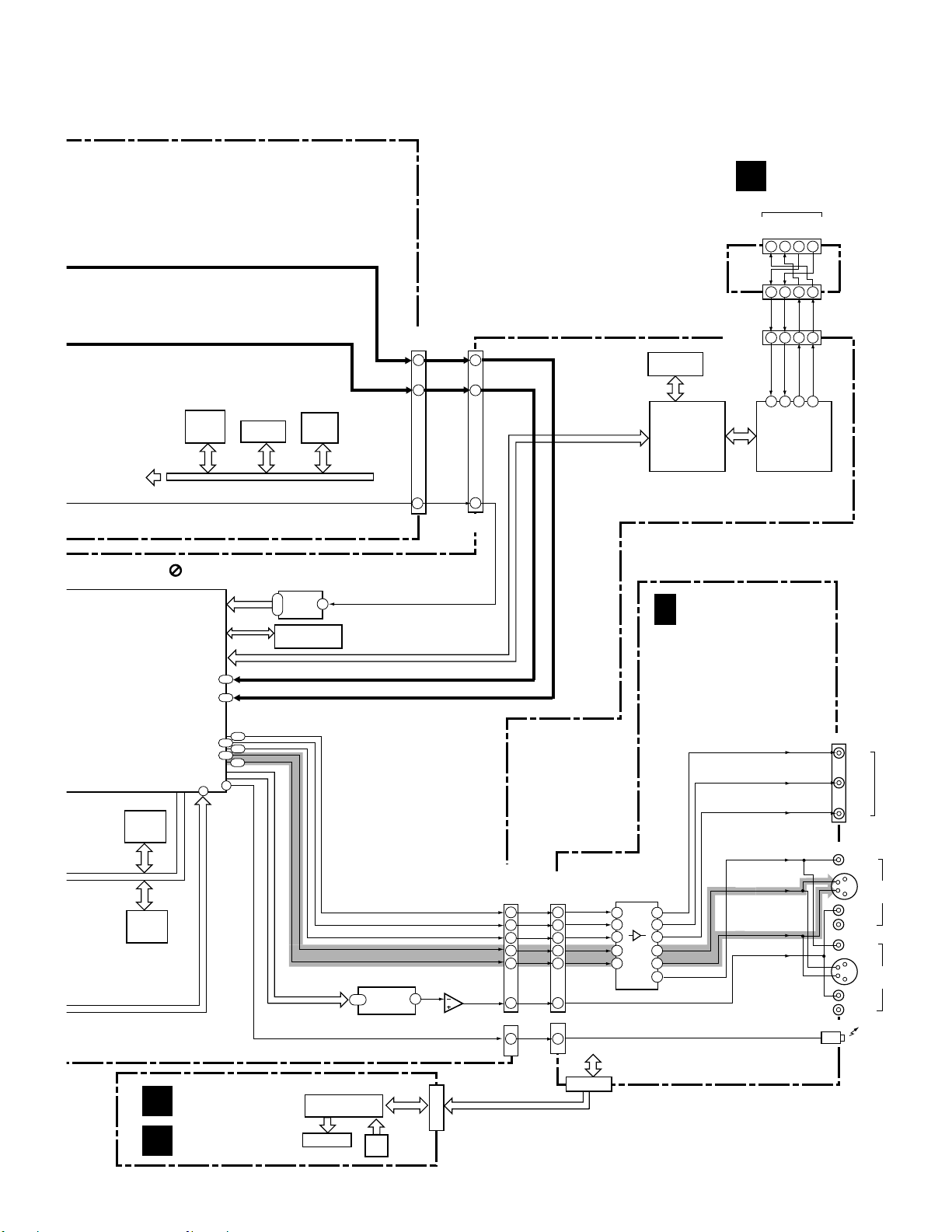
Recording Preview Mode
8
SIGNAL FLOW
DVD-R/RW Drive
Hard Disk Drive
ATA
SDRAM
Frame
AV-Enc.
ATA I/F
256Mb
TBC
ENC
128Mb
SDRAM
3D Y/C
DNR
(REC)
AV-codec
LSI
M65672WG
DEC
64Mb
SDRAM
1394 Link
DV-codec
Video
ADC
PAL/NTSC
Decoder
32bit RISC
CPU
1394
Phy.
SRC
Audio
A/D
S
1
F
B
S
Stereo
Video
Input
Selector
Audio
U
P
C
D
R
A
M
M
8
2
b
A
S
L
H
M
b
4
6
k
c
a
p
u
A
R
M
M
b
4
Decoder
Tuner/FL
Control CPU
TV
Tuner
Line-In
Select
INPUT
OUTPUT
AV-Dec.
Graphics
Engine
3D DNR
(PB)
Progressive
Converter
Video
DAC
PAL/NTSC
Encoder
Audio
D/A
Y/C/CVBS Video Out
Y/Cb/Cr Video Out
Audio Analog Out
DIF Out (Opt.)

Signal flow Record Preview Mode
9
In the normal viewing mode (non record) or recording modes the video signal passes
through the AV-codec IC on the main board with very little processing visible at the
monitor output.
If the user selects Preview Mode the video output at the monitor will show the
effects of all encoding, 3D Y/C separation, decoding and record mode settings.
This preview mode was designed to provide the user a way of viewing the record
quality prior to making a disc.
All models have the capability to select different recording quality based on time
from one to six hours.
LAYOUT
10
Power Supply
Power Supply
Unit
Unit
BOARD LAYOUT
REAR
REAR
FAN
FAN
JCKB ASSY
JCKB ASSY
TUNER
TUNER
Front--
Front
TUNB ASSY
TUNB ASSY
end
end
MAIN ASSY
MAIN ASSY
(under HDD)
(under HDD)
FRJB ASSY
FRJB ASSY
Writer Unit
Writer Unit
Æ
DRIVE ASSY R7 (520H)
Æ
DRIVE ASSY R7 (520H)
Æ
DRIVE ASSY R7R (320)
Æ
DRIVE ASSY R7R (320)
8mm space
8mm space
420mm
420mm
FRONT
FRONT
HDD
HDD
80GB (520H)
80GB (520H)
160GB (720H)
160GB (720H)
FL
FL
FLKY
FLKY
ASSY
ASSY
mm
mm
59
59
Æ
Æ
69
69
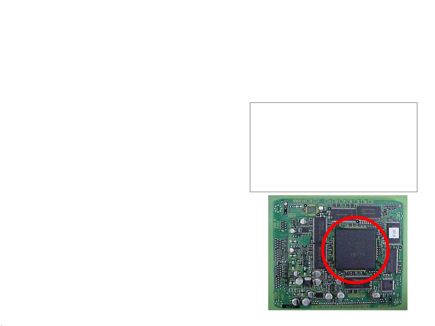
MAIN BOARD
11
1 Chip CODEC LSI (M65672WG)
MAIN FUNCTIONS
・ 10bit*27MHz(1ch),8bit*27MHz(3ch) Video ADC
・ PAL/NTSC Decoder
Process
・ 3-Dimensional YC Separation
Æ 0.13μm、CMOS 6 Layers (6Cu)
・ Frame TBC
・ 3-Dimensional DNR
・ MPEG Video Encoder
・ Dolby Digital Consumer Encoder
・ Graphics Engine (OSD, Scaling, Mixing)
・ MPEG Video Decoder
・ Audio Decoder (AC-3, MPEG)
・ PAL/NTSC Encoder
・ 10bit*54MHz(5ch) Video DAC
・ Progressive Conversion
・ Audio I/F
・ Drive I/F(ATA/ATAPI, 2ch)
・ Main CPU (32bit RISC, 54MHz)
Gate Scale
Æ about 4 million gate (Except memory)
Supply voltage
Æ Internal 1.2V, External 3.3V (Voltage-proof 5V)
Package
Æ 576pin PBGA
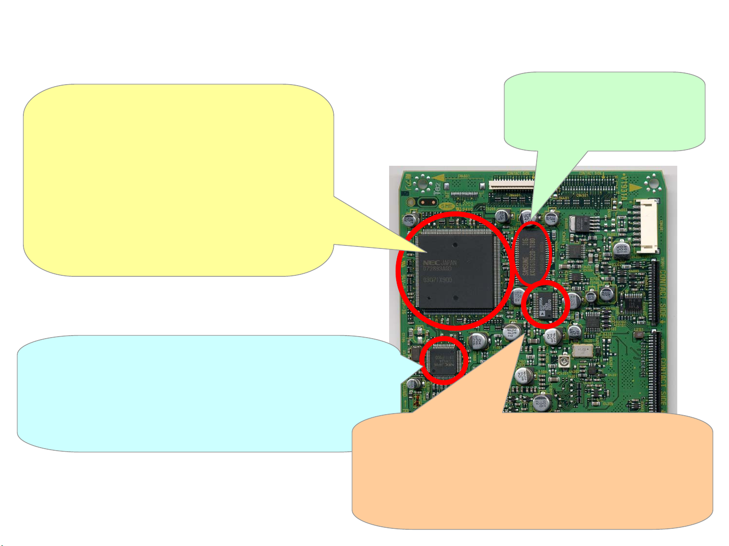
DV Device
12
1. DV CODEC / IEEE1394 Link LSI (IC5202)
Voltage I/O: 3.3V
Internal: 2.5V
Function DV Decode
DV Encode
IEEE1394 Link Layer Control
IEC61883 AV/C Command Control
(The control command sending
function to a DV camcorder etc.)
CPU (For IEEE1394 processing)
MAIN BOARD
IC5204
IC5204
DV SDRAM
DV SDRAM
Function: Working area for
Function: Working area for
DV link and the
DV link and the
codec
codec
2. IEEE1394 PHY LSI (IC5101)
Voltage 3.3V
Function IEEE1394 conformity physical layer control LSI
24.576MHz (PLL for IEEE1394)
built-in Crystal oscillation circuit
(Crystal oscillator is external)
3. Audio Sampling Rate Converter (IC3301)
Voltage 3.3V
Function the following sampling rates are converted
in order to absorb frequency deflection.
48kHz (DV Clock) Æ 48kHz (Recorder Clock)
32kHz (DV Clock) Æ 48kHz (Recorder Clock)
HDD UNIT
13
Factory Installed Built-In HDD’s could be one of three models. Replacement will be limited to one type.
1. TYPE
< DVR-520H-S > < DVR-65H-S >
VXF1010 80GB VXF1028 160GB
VXF1043 80GB (NSP) VXF1055 160GB (NSP)
VXF1036 80GB (NSP) VXF1040 160GB (NSP)
2. Other Info
MODEL PART#
VXF1010 5,400 Replacement
DVR-520H-S
DVR-65H-S
VXF1043 7,200 Factory
VXF1036 7,200 Factory
VXF1028 7,200 Replacement
VXF1055 7,200 Factory
VXF1040 7,200 Factory
ROTATIONAL SPEED
REMARKS
[rpm]
Maxtor
Western Digital
Seagate
Maxtor
Western Digital
Seagate

Overall Block
Diagrams
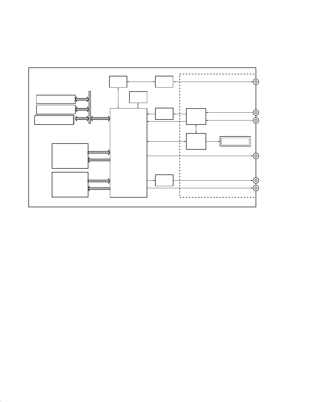
System configuration
15
DVR-520H-S
DVR-520H-S , DVR-320-S & DVR-65H-S
In each signal-processing LSI of the main function blocks,
various processes have been integrated into one chip, which
enables simpler system configuration. With the AV-signalprocessing LSI at the center, video inputs/outputs, audio
inputs/outputs, DV inputs/outputs, writer and various
memory cells are connected to it.
IC1102
Flash
IC1103
SRAM
IC1101, IC1201, IC1301
IC1401 SDRAM
Drive Assy
(DVD-R/RW)
HDD
UPD72893BGD-LML
Playback
Record
Playback
Record
UPD72852AGB-8EU
IC5202
1394 Link /
DV Codec
IC3301
SRC
IC1001
AV Signal
Processing
LSI
Fig2. System configuration
IC5101
1394 Phy
IC3101
Audio A/D
AK5357VT
IC3201
Audio D/A
PCM1742KE
Video : IC701 LA73033
Audio : IC601 LC75342M
Tuner / Line
Select
IC202
Tuner / FL
Control
CPU
1394 (DV)
FL
CVBS/YC/YCbCr
Analog Audio
DIF
[Memorized Data]
• EEPROM (IC204 JCKB ASSY)
The information about Tuner is backed up.
(Pre-set CH, AFT ON/OFF, Skip CH, etc)
Information about timed recording
Other information
(The state of Volume, remote control mode and
last positions (Line/Tuner, etc)
• CPU SDRAM (IC1101 MAIN ASSY)
The execution area and working area of a program
• FLASH ROM (IC1102 MAIN ASSY)
The storing area of a program code and setting information
• SRAM (IC1103 MAIN ASSY)
The working area for record and the storing area of setting
information (backup RAM)
• DEC SDRAM (IC1201 MAIN ASSY)
The working area of MPEG playback and OSD/Thumbnail
(OSD is mainly for Disc Menu creation in Video mode)
• ENC SDRAM (IC1301 MAIN ASSY)
The working area of MPEG recording and analog input and output (AVIO)
• ATA SDRAM (IC1401 MAIN ASSY)
The working area of ATA/OSD2/Audio TBC (OSD2 is for all GUI.)
• ATA SDRAM (IC1421 MAIN ASSY)
This is only for HDD model.
The working area about HDD operation.
• DV SDRAM (IC5204 MAIN ASSY)
The working area of Link and DV Codec
U301 VXF1022
16
Video
Audio
Audio
Video
DVR-520H-S
CD Audio
ANT
TV FRONT-END
RF IN
RF
OUT
IC451 CXA2020M
MPX
7
IN
ATT WIDEBAND SPECTRAL
F
VOUT
AOUT
16
Audio MPX
Decoder
CN1301
(15P)
19
6 8
FRJB
ASSY
Y/C
VIDEO
INPUT3
INPUT1
VIDEO
Y/C
INPUT3
VIDEO
Y/C
SPDL
MOTOR
JA1301
JA1302
L
R
L
R
L
R
STEPPIONG
JA601
LOADING
MOTOR
MOTOR
Y
C
Y
C
Y
C
Pickup
LD
DRIVE
PICKUP
ASSY
M
M
4
8
12
TUNB
A
ASSY
CN301
UVL UVL
L
21
(15P)
10
6
2
A
B
C
D
S4
S3
S2
S1
CN101
(45P)
5
4
3
2
33
34
35
36
38
37
40
39
CN501
(12P)
CN502
LPF
CN451
PB DVD/CD
OUT
CN705
CIN2
YIN2
VIN2
LIN2
VIN1
VIN3
YIN1
YIN3
CIN1
CIN3
LIN1
LIN3
UVV
17 3
CN401
7 7
(19P)
CN402
(13P)
(19P)
(13P)
B
JCKB ASSY(1/3)
IC301
M30700FKLGP
Writer
CPU
7-10
13-16
RF IC
IC101
UPC3330GC
6CH
Driver
IC501
BD7907FS
1/3
76
: Recording system signal route
UVV
19
2V
17
1V
15
3V
13
3Y
79
1Y
77
2Y
75
3C
7
1C
5
2C
3
LIN4
LIN2
LIN1
LIN3
HDD
DSP
IC201
201
DVD-VR
48
IC202
SDRAM
16Mbit
UPD63630GM
DRIVE ASSY
Video Selector
Video Driver
IC701
LA73033(1/2)
Audio Selector with Electirc ATT
CN401
(40P)
DVD-Video
11
13
14
12
1
8
CN4401
(40P)
IC601
LC75342M
CN4501
(40P)
DVD-VR
DVD-Video
C
MAIN ASSY
B
2/3
CD Digital
: Playback system signal route
V/Y
27
25
[ATAPI]
C
[ATA]
IC1421
IC1401
LPF
LPF
5
ATA SDRAM
256Mbit
JCKB ASSY
CN703
CN201
(2P)
CN702
(2P)
(2/3)
2
2
L
Flash
64Mbit
IC1102 IC1101
(1/2)
(21P)
V/Y
C
IC1001
M65673WG
1 Chip
System Codec
IC1103
SRAM
4Mbit
×2
CPU SDRAM
128Mbit
CN3001
(1/2)
CD Digital
13 13
(21P)
• R ch is same as L ch.
17
DVR-65H-S
DVR-520H-S
DVR-320-S
I
C202
PEG034A
Tuner
U-com
Control
Data
I
C204
BR24L32F-W
EEPROM
I
C203
RS5C372A
Real
Time
Clock
CN701(1/2)
(32P)
L
9
7
5
SEL.V/Y
SEL.C
SEL.L
9
7
5
CN2001
(32P)
IC5204
DV SDRAM
16Mbit
IC5202
UPD72893BGD-LML
IEEE1394
Link IC
J
DV TERMINAL
JA1401
CN1401
(7P)
1,3 2 6 7
CN5102
1,3 2 6 7
(7P)
38 39 37 36
UPD72852AGB-8EU
Physical IC
DVJB ASSY
XTPB
TPB
XTPA
TPA
1 2 3 4
TPA
TPB
XTPA
XTPB
IC5101
IEEE1394
Master Clock Freerun
• MPEG2 PS Encode
• AC-3/Linear PCM
Audio Encode
• 2ch ATA/ATAPI Interface
• MPEG2 PS Decode
• AC-3/MPEG1/Linear
PCM Audio Decode
IC1301
ENC
SDRAM
128Mbit
DEC
SDRAM
128Mbit
IC1201
D
F5
FLKY ASSY
AF23
AG25
IC3101
AK5357VT
9
Audio
10
12
C IN
T26
CVBS IN
V27
AG24
AD21
AE24
D2
2
A/D
48KHz 20Bit
Sampling Rate
Converter
IC1001 PT6315
FL Driver
IC3301
SM5950AM
IC3201
PCM1742KE
Audio
1-3
D/A Conv.
7
IC3251-1/2
UPC4570G2
B
CN2001
(2/2)
Cr/R
Cb/B
Y/G
Y
C
2
1
3
CN3001(2/2)
(32P)
21
23
25
29
27
17 17
SPDIF
1 1
(21P)
(21P)
CN701
(2/2)
(32P)
Cr OUT
21
Cb OUT
23
Y(G) OUT
25
29
27
L OUT
CN702(2/2)
Tuner U-com
Y OUT
C OUT
IC701
LA73033(2/2)
51
53
45
43
41
CN201
(19P)
60
56
58
63
65
68
JCKB ASSY(3/3)
3/3
Y(G)
Cb
Cr
Y
C
V
Y(G)
Cb
Cr
VOUT
YOUT
COUT
LOUT
JA701
JA702
Y
C
Y
C
JA651
Y(G)
Cb
Cr
VIDEO
LINE
OUT 1
L
R
VIDEO
LINE
OUT 2
L
R
OPTICAL
AC-3/PCM
DIGITAL
AUDIO
OUT
COMPONENT
VIDEO OUT
KIRB ASSY
E
V1001
Key
SW
CN1001
(19P)
FL

Adjustments
Test Modes
&
Service Modes
* It is not necessary to adjust the ASSY normaly when exchanging the ASSY. But the adjustment is
19
necessary when exchanging the Tuner Module and IC451 stereo decoder IC.
No. Adjustment Name
Stereo Decoder ATT adjustment
1
(Input system adjustment)
Adj. Point Measurement Point
VR453
Audio ouput (L)
(Rear panel)
Adjustment Value
370mVrms ± 18.5mV
Adjustment State
Input a signal of Mono 1kHz/100% modulation
to
terrestrial tuner input. /through output.
Stereo Decoder Wideband
2
adjustment (Input system adjustment)
Stereo Decoder Spectral adjustment
3
(Input system adjustment).
VR451
VR452
Audio ouputs (L/R)
(Rear panel)
Audio ouputs (L/R)
(Rear panel)
Best point of separation
≥30dB Note 1
Best point of separation
≥25dB Note 1
Input a signal of Stereo 300Hz/30% modulation
(NR-ON/L ch only) to terrestrial tuner input.
Note 2
Input a signal of Stereo 3kHz/30% modulation
(NR-ON) to terrestrial wave input. /through output
Note 2
Note 1 : The values for channel separation is defined as those having passed through the following filters :
100Hz – 10kHz : +0/–0.5dB
15.75kHz – 100kHz : -40dB or more
Note 2 : The adjustment No.2 and No.3 should be repeated 2 times for good adjustment.
(Steps : No.1 → No.2 →No.3 →No.2 →No.3)
TUNB ASSY
C326
R318
C327
R307
R306
VNP1963-A
C451
C462
VR452
C456
19
191
VR452
SEPA
ADJAST
SPECTRUM
C465
VR451
SEPA
ADJAST
VR451
WIDE
C471
FCICT
VR453
C453
R453
R454
C459
R455
1
INPUT
LAVEL
ADJAST
C458
1
V+9
C468
PC
VR453
GND
V+9
NP
543
PYKC F4X
C328
U301
C306
C305
C329
21
R317
R316
GND
JA301
R325
Q306
LF
or
R
C318
R315
C316
R328
VWV
R326
C319
V+5TU
L303
C301 C302
D301
R301
Q301
C309
1
D302
G-Link TUNB
NP
C313
C303
R324
R312
C304
Q302
L306
Q304
CN301
R463
C467
C461
C460
Q451
C474
R471
C472
CN451
R468
C473
13
13
KN300
E2B2C
C2BE
R467
R466
Fig.1 Adjustment Points (TUNB ASSY)
* It is not necessary to adjust the ASSY normaly when exchanging the ASSY, but confirm the data.
20
No. Adjustment Name
Master clock free-running adjustment
1
(Clock system adjustment)
C
MAIN ASSY
CN5102
1
Q1102
R1052
C4107
4
1
R4109
X4102
3
2
R4107
R4106
C1104
L1102
C2317
TP1067
TP14
TP15
TP49
TP50
TP4305
TP4304
8
2
R4305
1
CN4301
1
82
R4302
R1901
CN1901
TP48
28
R4306
8
R4303
R1903
71
TP4306
2
TP4301
R1902
R1905
R4307
TP4307
717
71717
2
8
R4304
TP4303
TP4302
R1904
C2333
7
C5132
L5103
L5104
L5101
L5105
L5106
L5102
D1111
C1114
C4106
R1111
C4105
R4105
C4102
8
1
IC4101
5
4
R4103
R4102
R4104
C4103
C4104
R4101
C2319
R2312
R2314
Q2312
R2313
C2301
R2307
R2201
R2202
C2209
C2204
C2202
Q2201
Q2202
R2203
C2205
R2204
C2201
Q2203
R2209
Q2204
R2305
C2206
R2334
R2208
R2333
R2332
R2331
4
3
C2332
IC2331
1
6
4
1
C2334
IC2301
58
R2306
C2311
R2409
R2502
17
28
R2408
TP2503
TP2502
TP2501
R2311
R2407
C5136
R2206
C2305
C4032
C5137
C5138
TP28
R2210
R2205
C2308
C2407
TP2504
R4110
Q2311
R2303
C2331
R4108
C2265
C2246
C2208
Q2403
C1061
R2266
R2252
Q2302
Q2301
TP2505
IC4007
R2304
C2222
R2207
D4002
TP4015
C4033
C4034
L1009
L1008
R1012
VR2104
R2112
VR2105
R1023
R2115 R1024
R2116
R5265
R2113
Q2105
C2106
R2105
R2102
Q2101
R2301
C2102
R2302
C2306
C2104
R2235
R2233
C2101
Q2222
R2239R2221
C1013
TP1031 TP1033
C2221
R4213
C2220
C2223
R2214
8
1
IC2211
5
4
R2308
C2302
1
8
IC2302
4
5
C2406
R2404
R2406
Q2402
R2411
R2405
TP2018
TP2506
R2025
R2040
Adj. Point Measurement Point
MAIN ASSY
VC4201
L5501
R5108
R5103
C5105
C5110
C5111
C1011
R1071
VR1002
C1032
R2114
R2109
Q2104
C2105
R2106
R2103
C2103
R2111
R2107
2
R1048
R1080
1
R4206
C4206
R4207
C2210
TP2020
R2412
TP2019
TP2001
R1021
Q2102
Q2103
TP1026
TP1032
8
3
R4202
4
C2405
TP2002
F5101
TP1060
7
R4211
R4212
IC4206
C1054
TP1002
TP1027
1
R4208
TP2003
C1031
R1022
R5107
R5106
R5105
R5104
TP1050
TP1051
R1011
TP1024
717
C4207
C2241
R2255
TP2021
IC3402 Pin8 (XTO)
(SM8707KV)
R5120
R5116
R5122
R5114
R5110
R5121
R5117
R5115
R5109
C5120
C5112
IC5101
C5113
R5113
R5112
C1003
C1510
C1509
C1004
C1002
C1028
C1037
C1034
R1006
C1055
L1003
C1035
C1030
R1005
VC4201
L1004
R2227
R5223
VC4201
R5222
TP4202
C4202
C4201
F4201
1
8
IC4205
4
5
C4210
D4202
D4201
R2254
R3270
TP2008
TP2009
X5101
R5125 R5126
C5119
C5118
R1009
C1041
L1005
R1004
C1036
C1038
R1074
3
R4201
X4201
R4210
4
R4204
R3271
R2011
TP2012
TP2011
C5102
C5101
33
48 1
C1014
VR1001
R1090
C1001
TP1041
C1508
C1016
C1025
C1027
R1034
C1017
C1018
C1019
C1012
C1021 C1048
C1022
C1023
C1029
C1026
C1024
C1056
TP1028
TP1029
TP1030
2
8
R104582R1043
R4205
L4201
1
C4208
C4209
5
C4203
R4209
Q2241
R2253
C2243
TP2022
R2027
R2047
TP2004
TP2006
TP2005
R5123
L4202
C5122
C1052
C1053
R2012
1732
6449
C1044
C1045
C1047
C1049
C1039
C5123
L1007
TP1013
TP1012
C3255
TP2016
C1042
R2013
16
R5124
R5127
L1001
C5127
C4211
C5124
R5130
C1059
2
1
C3251
TP2023
TP2013
R3108
R3107
R3106
R3105
C5125
R2014
C1006
C3107
R5132
C1060
R1066
TP2024
TP2014
C1058
C5103
R5128
R5129
C5126
R1003
L5502C5121
R5131
L1006
R2015
1
7
TP5106
R5289
R5290
R5285
R2026
TP2015
C5104
17
1
728
C1057
C1051C1005
R1031
R5273
1
R5274
7
R3104
9
16
C1050
TP2017
TP2025
R3024
R3023
R3022
R3003
Adjustment Value
27.000000MHZ
± 130Hz
R525117R5249
R5252
R5253
R5256
R5254
208
2
8
R5259
1717
R5261
TP3303
IC3301
R3309
C3101
C3105
R3103
IC3001
TP3013
TP3010
28
R5258
C3301
C3106
1
TP3009
C5204
R3304
R3409
828
C3302
F3401
C3102
10
C3004
TP3008
17
2
8
2
R5255
C5225
17
12
C5231
1
C3303
C3408
C3404
8
R3411
R3408
R3203
R3202
Q3201
R3205
IC4003 IC4005
R4004
TP3007
1
TP4008
C4010
F3102
IC3403
TP3006
28
R5250
17
C5213
C5230
C5229
R3410
5
C4013
R3204
R3406
1
Q3202
IC5202
C4014
IC4004
TP3005
C5214
R5262
R5263
R5260
R5257
1
C5216
C5215
R5272
2
8
2
28
1
R5275
7
8
C5217
R5276
R5286
R5277
R5287
R5288
R5278
28
R5279
R5280
R5281
52
R5282
53 104
R5283
C5218
R5284
R5296
R5295
R3303
13
R3310
R1008
R3307
R3311
R3312
24
R3306
R3313
R3305
L3301
C1040
R3102
C3108
8
IC3101
1
D3104
D3103
D3101
D3102
R3001R3025
D3001 D3002
11
C3002
20
C3001
R3002
TP3011
R5247
7
7
1
1
28
28
C5212
R5243
R5246
C5211
R5248
R5293 R5294
C5222
IC5204
R5298
C5224
TP3401
C3403
R3405
16
C3405
5
IC3402
F3403
1
4
C3407
C3402
IC3402 Pin8
F3402
4
3
C4018
C4006
TP4011
R2017
TP4012TP2007
Q2001
C4021
R4008
TP3002
TP3004
Adjustment State
No signal input
L5504
C5210
C5209
157
156
TP5201
TP5202
C5226
R5237
R5238
C5227
C5228
R5229
R5230
105
C5208
R5242
R5245
R5239
R5241
R5244
R5240
C5223
L5508
R5297
R3407
R3403
9
R4019
D4001
R4017
8
C4028
TP3403
C3406
R4020
TP3402
R2019
F4001
C4005
C4027
R4015
R4010
C4024
TP4002
TP4201
R4001
C4004
TP3014TP3001TP3003
TP3012
SIDE A
C5207
R5231
R5233
R5216
R5217
1
2
8
R5218
1
7
7
1
28
1728
R5220
7
17
28
R5313
1
R5314
728
L5507
TP5204
C5329
C5221
IC4008
R4018
TP4009
F4003
R4009
C4023
R5224
R5225
R5227
R5228
C5205
C5321
TP4001
TP4005
R4014
R5232
R5214
R5215
R5234
R5235
R5236
C4031
2
8
C5206
R4531
TP4010
R5219
R5221
R4504
17
R4405
17
R4406
1
7
R4407
71
R4408
R4428
R4429
R4432
R4435
1
R4507
7
1
R4508
7
R4509
71
R4510
1
7
1
7
TP32 TP38
TP31
2
8
28
2
8
CN4401
2
8
2
17
R4436
8
C4401
C4020
R4503
R4501
2
8
2
8
82
2
CN4501
8
R4530
R4534R4537
2
R4538
8
R4541
D4501
1
C4029
CN4001
8
TP41
TP40
TP42

Service Diagnosis List
21
CPRM ID NUMBER AND DATA SETTING
The Setting is necessary
• " CPRM ERR" is displayed on the FL display immediately after the power is turned on or in Stop mode.
• When the MAIN ASSY , DRIVE ASSY or the FLASH ROM is exchanged.
MODEL SETTING
DOWNLOAD METHOD
The Setting is necessary
• When the MAIN ASSY is replaced.
• When the JCKB ASSY is replaced.
• When the MAIN ASSY and JCKB ASSY is replaced.
SERVICE MODE
[First Screeen] (Version information, etc)
[Sub Screen 1] (Result of error-rate measurement : Video mode/VR mode)
[Sub Screen 2] (HDD information)
[Second Screen] (ATA/ATAPI debug screen)
[Sub Screen 3] (writer maintenance information of ATA/ATAPI DEBUG OSD)
[Sub Screen 4] (ATA/ATAPI DEBUG OSD_LD degradation judgement)
[Fourth Screen] (VR-recording error log)
[Sub Screen 4] (Error log for VR recording)
[Fifth Screen] (Error log for VR playback)
[Sub Screen 2] (Error log for VR playback)
DV DEBUG MODE
[Third Screeen] (DV debug information)
ERROR RATE MEASUREMENT
Only Video mode measurement
VIDEO ADJUSTMENT FOR SPECIFIC AREA
Purposes:
Depending on the area, jitter may appear in a picture received by the tuner, as conditions of signals received by
the tuner are different from area to area. To correct this kind of problem, the function of the System Codec AVIO
control section for adjusting signals received by the tuner can be used.
AGING MODE
CPRM ID NUMBER AND DATA SETTING
22
Entering the ID Number and ID Data for DVD Recorder
For the DVD recorder,it is necessary with the recoding/playback of DVD–RW disc to set an individual number (ID number) and ID data to
each recorder. If the number and data are not set correctly with the following procedure, operations in the future may not be guaranteed.
You will find the ID number to be set on the ID label on the rear panel.
Important: If no ID label is found on the rear panel, write down the specified ID number by checking it according to "How to
confirm the ID number" shown below.
The Input is Necessary When:
• " CPRM ERR" is displayed on the FL display immediately after the power is turned on or in Stop mode.
• When the MAIN ASSY , DRIVE ASSY or the HDD is exchanged.
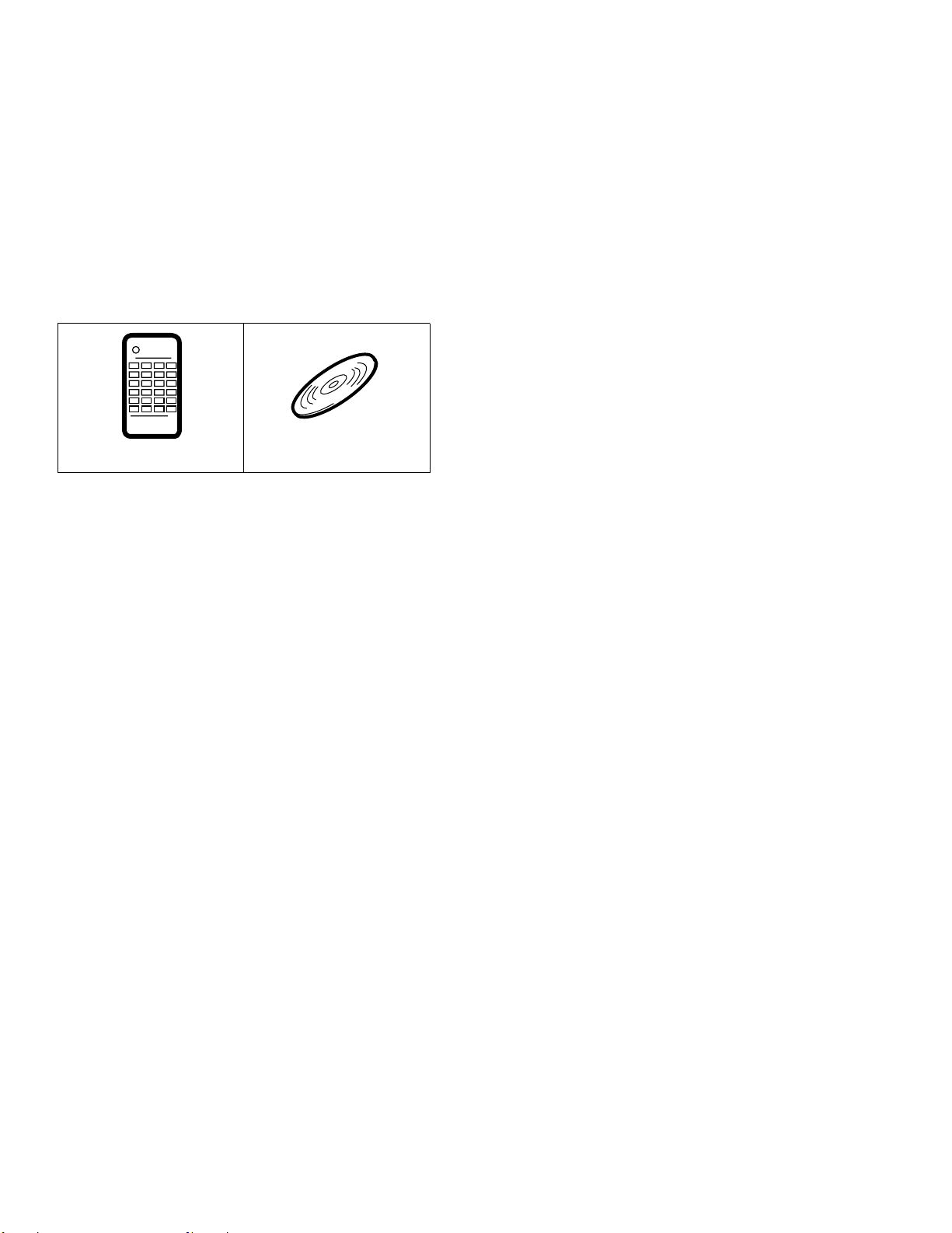
JIGS AND MEASURING INSTRUMENTS
Service Remote Control
Unit (GGF1381)
DVD Recorder Data Disc
(GGV1179)
(*) Refer to P138.
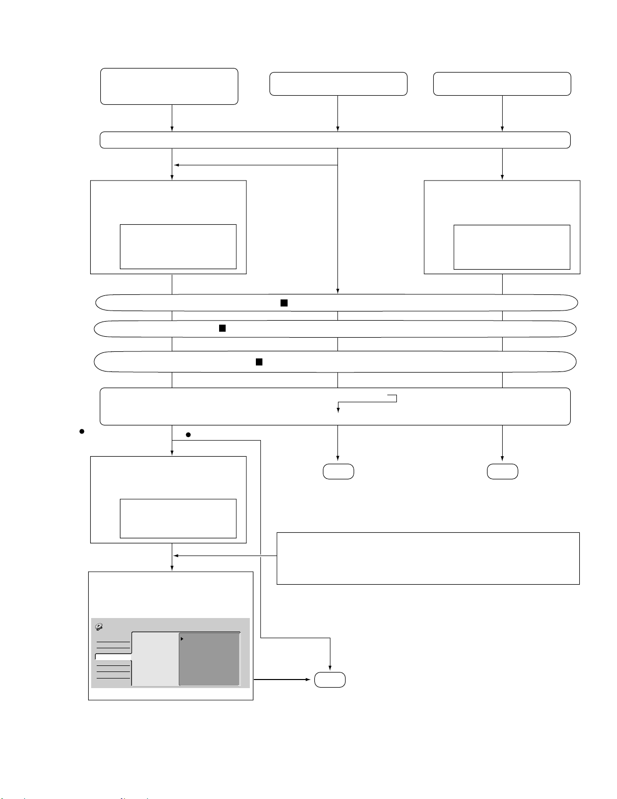
Input Flow of the ID No. and ID data when exchanging HDD, MAIN Assy or Drive Assy
23
DVR-65H-S
DVR-520H-S
DVR-65H-S
DVR-520H-S
• When exchanging HDD or MAIN
Assy, or both exchanged
• When exchanging HDD
Also exchanging DRIVE Assy simultaneously
When displayed following message at
Power on
FL Tube : [HDD ERR]
CRT display :
HDD information is not correct.
When exchanging Drive Assy
Power → ON
Only exchanging
Drive Assy
Confirmation of the CPRM ID No.
Deletion of the CPRM ID No.(when ID No. is registered.)
Input of the CPRM ID No. and ID data
When displayed "CPRM ERR"
When displayed following message at
Power on
FL Tube : [CPRM ERR]
CRT display :
CPRM information is not correct.
New HDD/when
there is error
on recorded contents
When displayed following message at
Power on
FL Tube : [HDD ERR]
CRT display :
HDD information is not correct.
Execute HDD Initialize from
the Disc Setup menu.
*Use Remote Control of
the model
Execute
HOME MENU → Disc Setup → Intialize
HDD → Start
Disc Setup
Basic
Initialize
Finalize
Initialize HDD
Initialize
Exchanging to the original HDD(when
there is no error on
the recorded
contents.)
Start
Power → OFF → ON
Normal operation mode
End
End
[CAUTION]
All recorded data are deleted if the HDD is intialized.
Take care that restoration of the user's data recorded on the HDD is totally
impossible.
Before servicing, OBTAIN THE USER'S PRIOR CONSENT to that effect.
*Goes to normal operation
with no caution
End
 Loading...