Pioneer DV-3500, DV-3501 Repair manual

DVD PLAYER
DV-3500
DV-3500-G
DV-3501
THIS MANUAL IS APPLICABLE TO THE FOLLOWING MODEL(S) AND TYPE(S).
Model Power Requirement
DV-3500 AC110-127V/220-240V 6
DV-3500-G AC110-127V/220-240V 6
DV-3501 AC110-127V/220-240V 6
RAMXU
RAMXU
RAMXU
Type
Regional restriction
codes (Region No.)
ORDER NO.
RRV2622
Remarks
¶ This service manual should be used together with the following manual(s):
Model No. Order No. Remarks
DV-353-K/KUXJ RRV2592
Confirm it
Serial No.
PIONEER CORPORATION 4-1, Meguro 1-chome, Meguro-ku, Tokyo 153-8654, Japan
PIONEER ELECTRONICS (USA) INC. P.O. Box 1760, Long Beach, CA 90801-1760, U.S.A.
PIONEER EUROPE NV Haven 1087, Keetberglaan 1, 9120 Melsele, Belgium
PIONEER ELECTRONICS ASIACENTRE PTE. LTD. 253 Alexandra Road, #04-01, Singapore 159936
PIONEER CORPORATION 2002
T – ZZE JUNE 2002 Printed in Japan

1
23
1. CONTRAST OF MISCELLANEOUS PARTS
NOTES : ÷ Parts marked by “ NSP ” are generally unavailable because they are not in our Master Spare Parts List.
A
÷ The
÷ Reference Nos. indicate the pages and Nos. in the service manual for the base model.
÷ When ordering resistors, first convert resistance values into code form as shown in the following examples.
B
7 CONTRAST TABLE
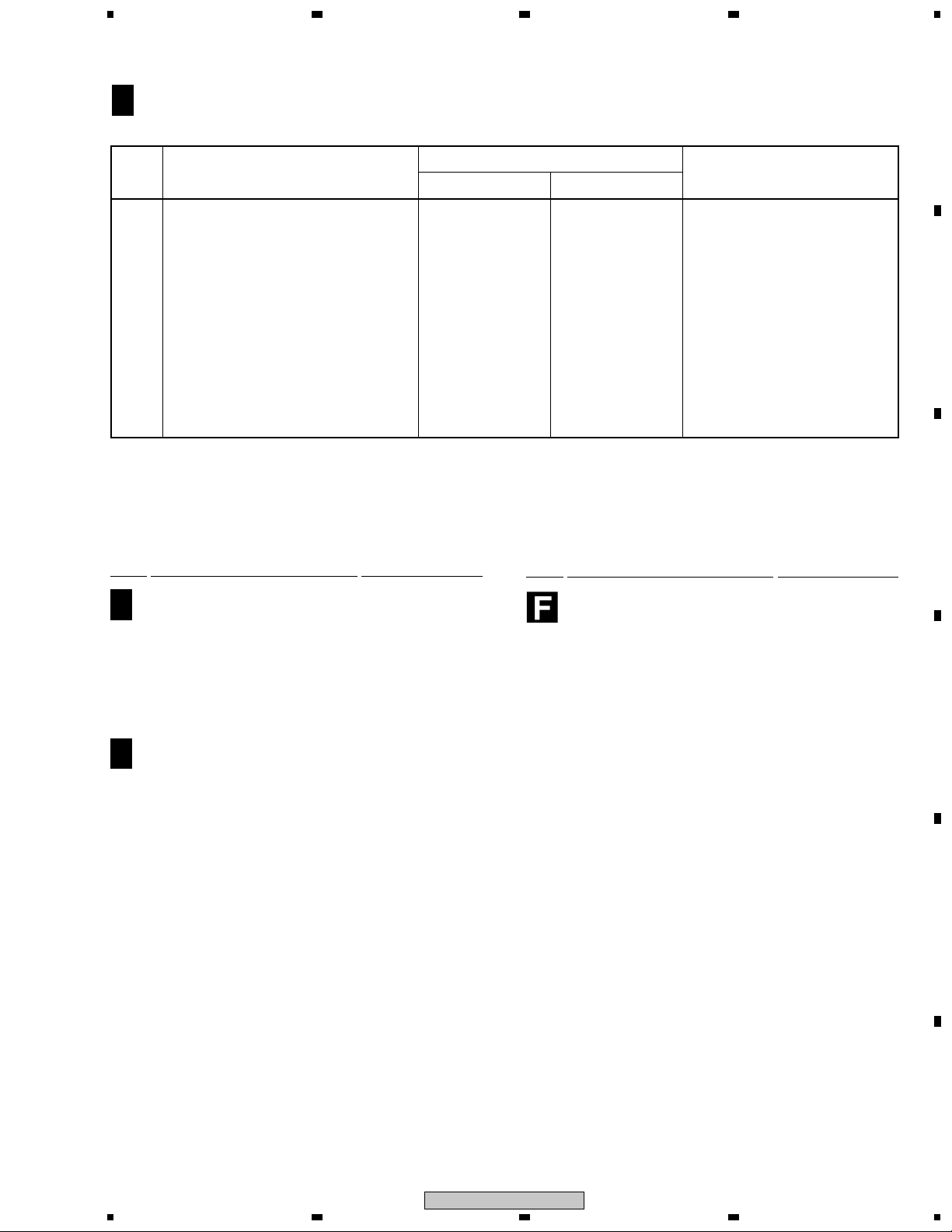
DV-3500/RAMXU, DV-3500-G/RAMXU, DV-3501/RAMXU and DV-353-S/KUXU/CA are constructed the same
except for the following:
Ref.
Mark
No.
C
P9 - 1 NSP IRKY ASSY VWG2344 VWG2344 VWG2344 VWG2344
P9 - 2 NSP PSWB ASSY VWG2345 VWG2345 VWG2345 VWG2345
NSP KEYB ASSY VWM2122 VWM2123 VWM2123 VWM2123
NSP DOUT ASSY Not used VWV1901 VWV1901 VWV1901 No. 1
mark found on some component parts indicates the importance of the safety factor of the part.
Therefore, when replacing, be sure to use parts of identical designation.
Ex. 1 When there are 2 effective digits (any digit apart from 0), such as 560 ohm and 47k ohm (tolerance is shown by
J = 5%, and K = 10%).
1
560 Ω = 56 × 10
47k Ω = 47 × 10
= 561 ................................................... RD1/4PU 5 6 1 J
3
= 473 .................................................. RD1/4PU 4 7 3 J
0.5 Ω = R50 ...................................................................... RN2H Â 5 0 K
1 Ω = 1R0 ......................................................................... RS1P 1 Â 0 K
Ex. 2 When there are 3 effective digits (such as in high precision metal film resistors).
5.62k Ω = 562 × 10 1 = 5621 ........................................... RN1/4PC 5 6 2 1 F
Part No.
Symbol and Description
DV-353-S DV-3500 DV-3500-G DV-3501
KUXU/CA RAMXU RAMXU RAMXU
PCB ASSEMBLIES
4
Remarks
P9 - 3 FJMB ASSY VWS1515 VWS1520 VWS1520 VWS1520
P9 - 7 > POWER SUPPLY Unit VWR1351 VWR1352 VWR1352 VWR1352
(or VWR1353) (or VWR1354) (or VWR1354) (or VWR1354)
PACKING
P7 - 1 > Power Cable ADG7022 ADG7018 ADG7018 ADG7018
D
E
P7 - 2 NSP Warranty Card ARY7057 ARY7046 ARY7046 ARY7046
P7 - 3 NSP AA/R6P Dry Cell Battery VEM1010 VEM1030 VEM1030 VEM1030
P7 - 5 Operating Instructions (English) VRB1285 Not used Not used Not used
P7 -12 Packing Case VHG2169 VHG2184 VHG2265 VHG2266
Operating Instructions (Simp-Chinese) Not used VRC1148 VRC1148 VRC1148
EXTERIOR SECTION
P9 -13 Rear Panel VNA2437 VNA2448 VNA2512 VNA2513
P9 -15 DVD V Plate VAM1121 VAM1120 VAM1123 VAM1121
P9 -18 Tray Panel VNK4973 Not used Not used VNK5042
P9 -19 Front Panel Assy VXA2496 VXA2512 VXA2535 VXA2536
P9 -20 Pioneer Badge VAM1129 VAM1129 VAM1112 VAM1112
P9 -21 NSP Energy Star Label AAX7876 Not used Not used Not used
P9 -26 Bonnet Case S VXX2823 VXX2823 VXX2820 VXX2820
Flexible Cable (08P) Not used VDA1887 VDA1887 VDA1887 No. 2
Tray Panel Assy Not used VXA2506 VXA2540 Not used No. 3
Tray Panel Not used VNK4979 VNK5145 Not used No. 4
Sub Panel Not used VNK4977 VNK4977 Not used No. 5
Label (Rear) Not used VRW1739 VRW1739 VRW1739 for Rear Panel
RAM Caution Label Not used VRW1904 VRW1904 VRW1904 for Bonnet
• The numbers in the remarks column correspond to the numbers on the “EXPLODED VIEWS”.
F
• For PCB assemblies, Refer to “CONTRAST OF PCB ASSEMBLIES”, “PCB PARTS LIST”, “2. SCHEMATIC DIAGRAM” and “3. PCB CONNECTION
DIAGRAM”.
2
1234
DV-3500

5
678
7 CONTRAST OF PCB ASSEMBLIES
B
FJMB ASSY
F
VWS1520 and VWS1515 are constructed the same except for the following:
A
Mark Symbol and Description
IC301 L6315ATXXTY L6315ATXXT
IC603 VYW1978 VYW1963
C733, C753 CKSRYB272K50 CCSRCH331J50
C734, C754 VCH1226 (330P/50V) CCSRCH330J50
R27 RS1/16S333J RS1/16S562J
R28 RS1/16S562J RS1/16S333J
R731, R751 RN1/16SE2201D RN1/16SE1602D
R733, R753 RS1/16S102J RS1/16S223J
R734, R754 RN1/16SE4301D RN1/16SE2702D
R736, R737, R756, R757 RS1/16S471J RS1/16S221J
CN902 CONNECTOR Not used 52045-0845 ∗1
∗1: Refer to “2. SCHEMATIC DIAGRAM”.
7 PCB PARTS LIST
Mark No. Description Part No.
Part No.
Remarks
VWS1515 VWS1520
B
C
Mark No. Description Part No.
E
POWER SUPPLY UNIT (VWR1352)
F
OTHERS
> P103 PROTECTOR (1.6A) AEK7012
> P101 PROTECTOR (800mA) AEK7063
> P102 PROTECTOR (1.6A) AEK7066
> P104 PROTECTOR (2A) AEK7067
> F1 FUSE (2A) REK1101
E
F
POWER SUPPLY UNIT (VWR1354)
OTHERS
> CP5 PROTECTOR (800mA) AEK7063
> CP2, CP3 PROTECTOR (1.6A) AEK7066
> CP1 PROTECTOR (2A) AEK7067
> F1 FUSE (2.5A) REK1102
DOUT ASSY
COILS AND FILTERS
L201, L251 CHIP BEADS VTL1089
CAPACITORS
C151 CEAT102M6R3
C201, C251 CEAT471M6R3
RESISTORS
R152, R202, R252 RS1/16S75R0F
OtherResistors RS1/16S###J
OTHERS
CN101 CONNECTOR 52045–0845
CN102 D-SOCKET(14P) AKP7137
D
E
F
DV-3500
5
6
7
8
3

1
No. 1
No. 2
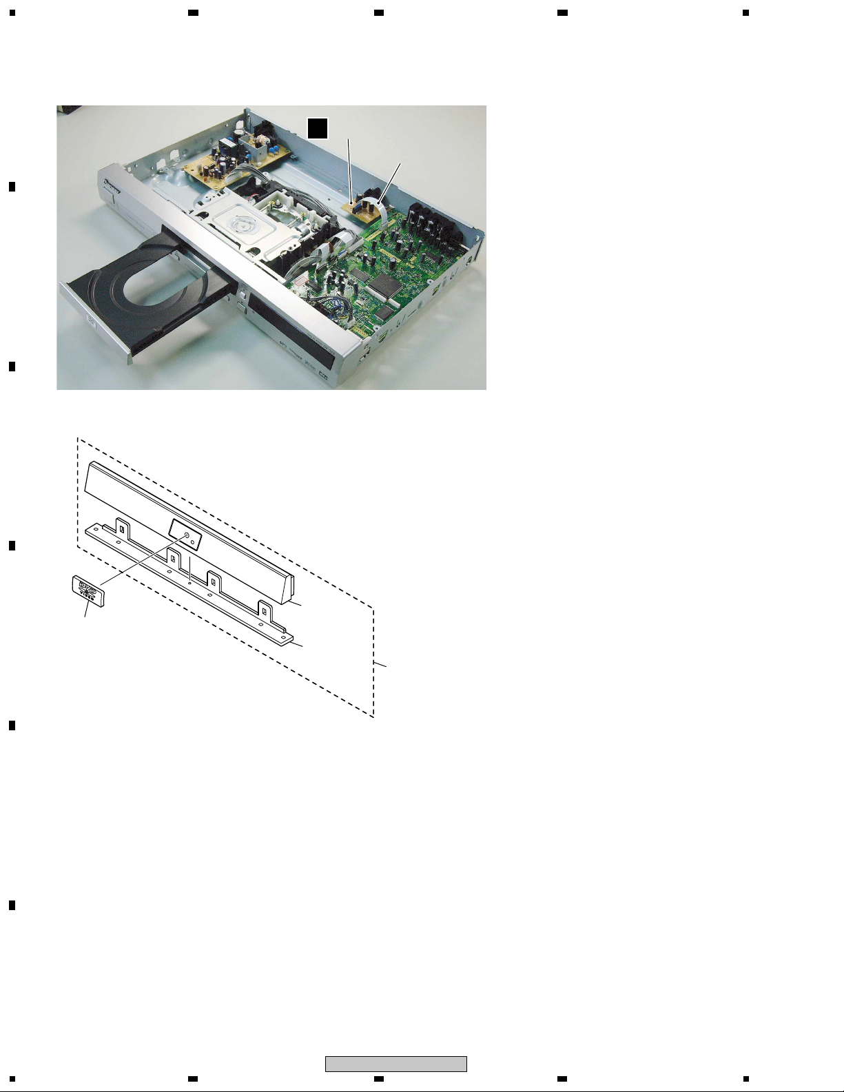
7 EXPLODED VIEWS
÷
A
B
EXTERIOR SECTION
23
No. 1
No. 1
F
No. 2
No. 2
4
C
No. 3- 5: DV-3500 and DV-3500-G Only
No. 4
D
DVD V Plate
No. 5
No. 3
E
F
4
1234
DV-3500
