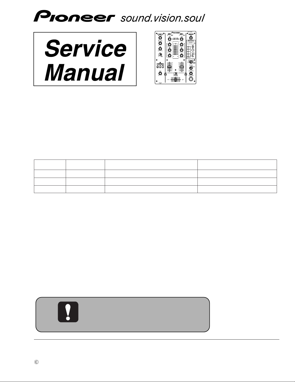
Pioneer DJM-400 Service manual
PIONEER CORPORATION 4-1, Meguro 1-chome, Meguro-ku, Tokyo 153-8654, Japan
PIONEER ELECTRONICS (USA) INC. P.O. Box 1760, Long Beach, CA 90801-1760, U.S.A.
PIONEER EUROPE NV Haven 1087, Keetberglaan 1, 9120 Melsele, Belgium
PIONEER ELECTRONICS ASIACENTRE PTE. LTD. 253 Alexandra Road, #04-01, Singapore 159936
PIONEER CORPORATION 2006
4
ORDER NO.
RRV3351
DJM-400
DJ MIXER
DJM-400
THIS MANUAL IS APPLICABLE TO THE FOLLOWING MODEL(S) AND TYPE(S).
Model Type Power Requirement Remarks
DJM-400 KUCXJ AC 120V
DJM-400 RLXJ AC 110-120V / 220-240V
DJM-400 WYXJ5 AC 220-240V
For details, refer to "Important Check Points for good servicing".
T-IZY MAR. 2006 printed in Japan
1234
SAFETY INFORMATION
A
This service manual is intended for qualified service technicians ; it is not meant for the casual do-ityourselfer. Qualified technicians have the necessary test equipment and tools, and have been trained
to properly and safely repair complex products such as those covered by this manual.
Improperly performed repairs can adversely affect the safety and reliability of the product and may
void the warranty. If you are not qualified to perform the repair of this product properly and safely, you
should not risk trying to do so and refer the repair to a qualified service technician.
WARNING
This product contains lead in solder and certain electrical parts contain chemicals which are known to the state of California to
B
cause cancer, birth defects or other reproductive harm.
NOTICE
(FOR CANADIAN MODEL ONLY)
Fuse symbols (fast operating fuse) and/or (slow operating fuse) on PCB indicate that replacement parts must
be of identical designation.
Health & Safety Code Section 25249.6 - Proposition 65
REMARQUE
(POUR MODÈLE CANADIEN SEULEMENT)
Les symboles de fusible (fusible de type rapide) et/ou (fusible de type lent) sur CCI indiquent que les pièces
de remplacement doivent avoir la même désignation.
C
(FOR USA MODEL ONLY)
1. SAFETY PRECAUTIONS
The following check should be performed for the
continued protection of the customer and service
technician.
ANY MEASUREMENTS NOT WITHIN THE LIMITS
OUTLINED ABOVE ARE INDICATIVE OF A POTENTIAL
SHOCK HAZARD AND MUST BE CORRECTED BEFORE
RETURNING THE APPLIANCE TO THE CUSTOMER.
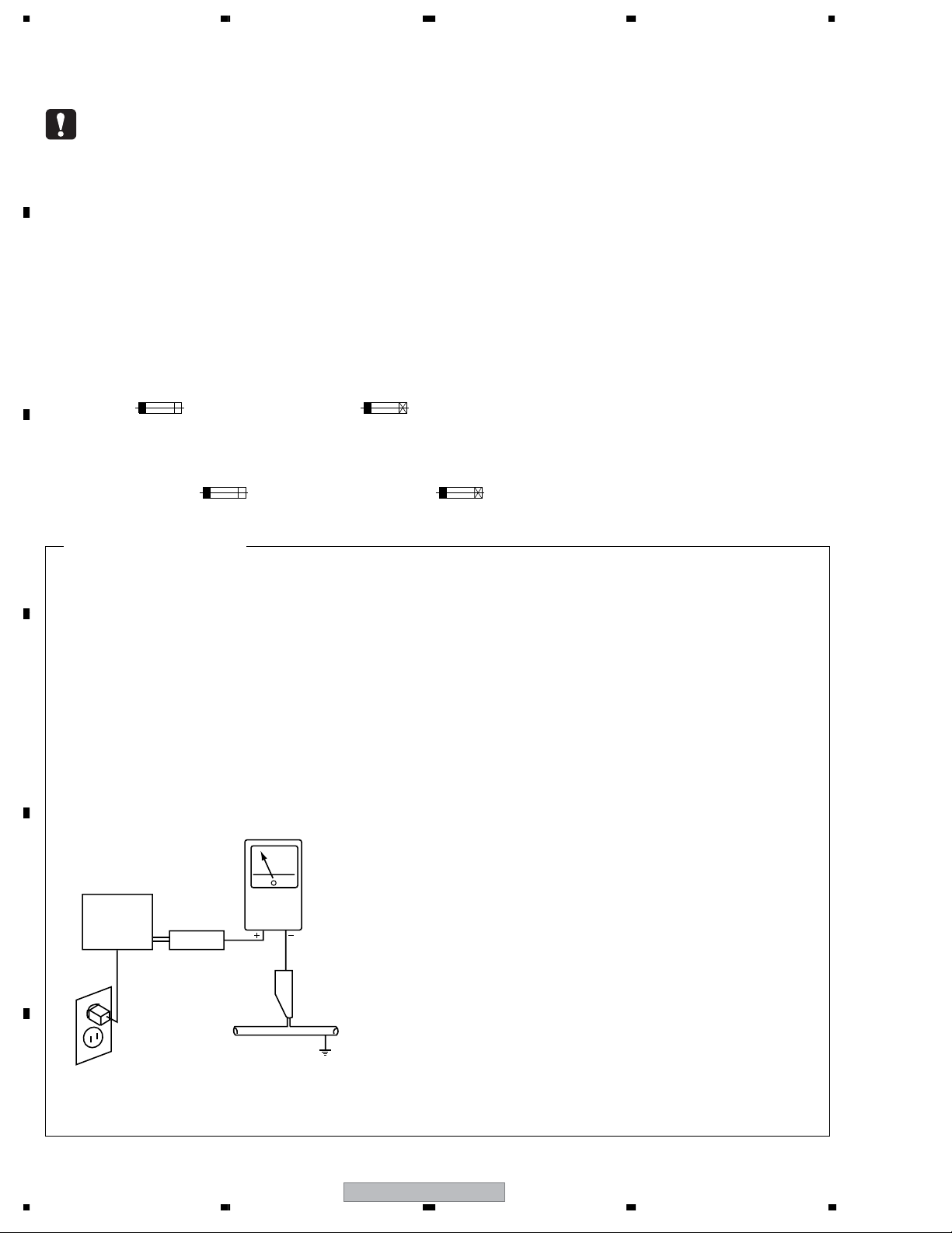
LEAKAGE CURRENT CHECK
Measure leakage current to a known earth ground
(water pipe, conduit, etc.) by connecting a leakage
D
E
current tester such as Simpson Model 229-2 or
equivalent between the earth ground and all exposed
metal parts of the appliance (input/output terminals,
screwheads, metal overlays, control shaft, etc.). Plug
the AC line cord of the appliance directly into a 120V
AC 60 Hz outlet and turn the AC power switch on. Any
current measured must not exceed 0.5 mA.
Reading should
not be above
0.5 mA
Earth
ground
Device
under
test
Also test with
plug reversed
(Using AC adapter
plug as required)
Leakage
current
tester
Test all
exposed metal
surfaces
2. PRODUCT SAFETY NOTICE
Many electrical and mechanical parts in the appliance
have special safety related characteristics. These are
often not evident from visual inspection nor the protection
afforded by them necessarily can be obtained by using
replacement components rated for voltage, wattage, etc.
Replacement parts which have these special safety
characteristics are identified in this Service Manual.
Electrical components having such features are
identified by marking with a > on the schematics and on
the parts list in this Service Manual.
The use of a substitute replacement component which
does not have the same safety characteristics as the
PIONEER recommended replacement one, shown in the
parts list in this Service Manual, may create shock, fire,
or other hazards.
Product Safety is continuously under review and new
instructions are issued from time to time. For the latest
information, always consult the current PIONEER Service
Manual. A subscription to, or additional copies of,
PIONEER Service Manual may be obtained at a nominal
charge from PIONEER.
F
2
AC Leakage Test
DJM-400
1234
5678
[Important Check Points for Good Servicing]
In this manual, procedures that must be performed during repairs are marked with the below symbol.
Please be sure to confirm and follow these procedures.
1. Product safety
Please conform to product regulations (such as safety and radiation regulations), and maintain a safe servicing environment by
following the safety instructions described in this manual.
1 Use specified parts for repair.
Use genuine parts. Be sure to use important parts for safety.
2 Do not perform modifications without proper instructions.
Please follow the specified safety methods when modification(addition/change of parts) is required due to interferences such as
radio/TV interference and foreign noise.
3 Make sure the soldering of repaired locations is properly performed.
When you solder while repairing, please be sure that there are no cold solder and other debris.
Soldering should be finished with the proper quantity. (Refer to the example)
4 Make sure the screws are tightly fastened.
Please be sure that all screws are fastened, and that there are no loose screws.
5 Make sure each connectors are correctly inserted.
Please be sure that all connectors are inserted, and that there are no imperfect insertion.
6 Make sure the wiring cables are set to their original state.
Please replace the wiring and cables to the original state after repairs.
In addition, be sure that there are no pinched wires, etc.
7 Make sure screws and soldering scraps do not remain inside the product.
Please check that neither solder debris nor screws remain inside the product.
8 There should be no semi-broken wires, scratches, melting, etc. on the coating of the power cord.
Damaged power cords may lead to fire accidents, so please be sure that there are no damages.
If you find a damaged power cord, please exchange it with a suitable one.
9 There should be no spark traces or similar marks on the power plug.
When spark traces or similar marks are found on the power supply plug, please check the connection and advise on secure
connections and suitable usage. Please exchange the power cord if necessary.
0 Safe environment should be secured during servicing.
When you perform repairs, please pay attention to static electricity, furniture, household articles, etc. in order to prevent injuries.
Please pay attention to your surroundings and repair safely.
A
B
C
D
2. Adjustments
To keep the original performance of the products, optimum adjustments and confirmation of characteristics within specification.
Adjustments should be performed in accordance with the procedures/instructions described in this manual.
3. Lubricants, Glues, and Replacement parts
Use grease and adhesives that are equal to the specified substance.
Make sure the proper amount is applied.
4. Cleaning
For parts that require cleaning, such as optical pickups, tape deck heads, lenses and mirrors used in projection monitors, proper
cleaning should be performed to restore their performances.
5. Shipping mode and Shipping screws
To protect products from damages or failures during transit, the shipping mode should be set or the shipping screws should be
installed before shipment. Please be sure to follow this method especially if it is specified in this manual.
56
DJM-400
E
F
3
7
8

1234
CONTENTS
1. SPECIFICATIONS ............................................................................................................................................ 5
2. EXPLODED VIEWS AND PARTS LIST ............................................................................................................ 6
A
B
C
D
2.1 PACKING SECTION .................................................................................................................................. 6
2.2 EXTERIOR SECTION................................................................................................................................ 8
2.3 CONTROL PANEL SECTION .................................................................................................................. 10
3. BLOCK DIAGRAM AND SCHEMATIC DIAGRAM ..........................................................................................12
3.1 BLOCK DIAGRAM ................................................................................................................................... 12
3.1.1 OVERALL BLOCK DIAGRAM ........................................................................................................... 12
3.1.2 CPU & DSP BLOCK DIAGRAM ........................................................................................................13
3.2 OVERALL WIRING DIAGRAM................................................................................................................. 14
3.3 MAIN ASSY (1/3) ..................................................................................................................................... 16
3.4 MAIN ASSY (2/3) ..................................................................................................................................... 18
3.5 MAIN ASSY (3/3) ..................................................................................................................................... 20
3.6 JACK ASSY (1/4)..................................................................................................................................... 22
3.7 JACK ASSY (2/4)..................................................................................................................................... 24
3.8 JACK ASSY (3/4)..................................................................................................................................... 26
3.9 JACK (4/4) and HP ASSYS...................................................................................................................... 28
3.10 MIC ASSY.............................................................................................................................................. 30
3.11 TRANS ASSY ........................................................................................................................................ 31
3.12 VRSW (1/3) and CHRV ASSYS............................................................................................................. 32
3.13 VRSW ASSY (2/3) .................................................................................................................................34
3.14 VRSW (3/3), FADER and CFVR ASSYS ............................................................................................... 36
3.15 VOLTAGES............................................................................................................................................. 38
3.16 WAVEFORMS........................................................................................................................................ 41
4. PCB CONNECTION DIAGRAM ..................................................................................................................... 50
4.1 MAIN ASSY ............................................................................................................................................. 50
4.2 JACK, HP and MIC ASSYS .....................................................................................................................52
4.3 VRSW and CHRV ASSYS ....................................................................................................................... 56
4.4 FADER, CFVR and TRANS ASSYS ........................................................................................................ 60
5. PCB PARTS LIST ........................................................................................................................................... 62
6. ADJUSTMENT ............................................................................................................................................... 65
7. GENERAL INFORMATION............................................................................................................................. 66
7.1 DIAGNOSIS ............................................................................................................................................. 66
7.1.1 TEST MODE ...................................................................................................................................... 66
7.1.2 Rewriting of the Software................................................................................................................... 72
7.1.3 POWER-ON SEQUENCE .................................................................................................................74
7.1.4 DISASSEMBLY.................................................................................................................................. 75
7.2 PARTS...................................................................................................................................................... 81
7.2.1 IC ....................................................................................................................................................... 81
8. PANEL FACILITIES ........................................................................................................................................ 88
8.1 CONNECTION PANEL SECTION............................................................................................................ 88
8.2 CONTROL PANEL SECTION .................................................................................................................. 89
E
F
4
1234
DJM-400
5678
1. SPECIFICATIONS
1.General
Power source
...........................................................................AC 120 V, 60 Hz
(KUCXJ model)
..........................AC 110 V to 120 V/220 V to 240 V, 50 Hz/60 Hz
(RLXJ model)
..................................................AC 220 V to 240 V, 50 Hz/60 Hz
(WYXJ5 model)
Power consumption...................................................................13 W
Operating temperature....................+5°C to +35°C (+41°F to +95°F)
Operating humidity....................5 % to 85 % (without condensation)
Weight........................................................................3.2 kg (7.05 lb)
Maximum dimensions..............223 (W) × 304.7 (D) × 106.6 (H) mm
8-3/4 (W) × 12 (D) × 4-3/16 (H) inch
2. Audio section
Sampling rate........................................................................ 96 kHz
A/D, D/A converter...................................................................24 bits
Frequency response
LINE....................................................................20 Hz to 20 kHz
MIC.....................................................................20 Hz to 20 kHz
PHONO...................................................20 Hz to 20 kHz (RIAA)
S/N ratio (at rated output)
LINE....................................................................................97 dB
PHONO...............................................................................82 dB
MIC.....................................................................................78 dB
Distortion (LINE-MASTER OUT)..........................................0.007 %
Input level/ Impedance
PHONO................................................................–52 dBu/47 kΩ
MIC 1, MIC 2........................................................–52 dBu/47 kΩ
CD, LINE..............................................................–12 dBu/47 kΩ
Output Level/Impedance
MASTER OUT..........................................................+2 dBu/1 kΩ
PHONES...............................................................+ 2 dBu/150 Ω
Crosstalk (LINE).......................................................................78 dB
Channel equalizer response (Isolater)
HI...........................................................+9 dB to –∞ (4.6 kHz )
MID............................................+9 dB to –∞ (284 Hz 4.6 kHz)
LOW........................................................+9 dB to –∞ ( 284 Hz)
Microphone equalizer response
HI..........–12 dB (full counterclockwise) to 0 dB (center) (10 kHz)
LOW.................–12 dB (full clockwise) to 0 dB (center) (100 Hz)
3. Input / output connector systems
PHONO/LINE input connectors
RCA pin jacks.............................................................................2
CD input connectors
RCA pin jacks.............................................................................2
MIC/AUX input connectors
Phone jacks (∅6.3 mm)..............................................................2
MASTER output connectors
RCA pin jacks.............................................................................2
PHONES connectors
Stereo phone jack (∅6.3 mm)....................................................1
CONTROL connectors
Mini-phone jacks (∅3.5 mm)......................................................2
4. Accessories
Operating Instructions......................................................................1
Power cord.......................................................................................1
Warranty card.................................................1 (KUCXJ model only)
Specifications and appearance are subject to change without
notice.
A
B
C
D
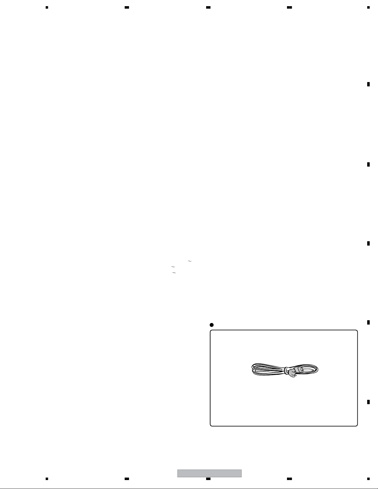
Accessories
Power cord
(KUCXJ : ADG7021)
(RLXJ, WYXJ5 : ADG1154)
Operating instructions
Warranty card (KUCXJ only)
DJM-400
56
E
F
5
7
8
1234
2. EXPLODED VIEWS AND PARTS LIST
NOTES:
A
Parts marked by "NSP" are generally unavailable because they are not in our Master Spare Parts List.
The mark found on some component parts indicates the importance of the safety factor of the part.
Therefore, when replacing, be sure to use parts of identical designation.
Screws adjacent to mark on product are used for disassembly.
For the applying amount of lubricants or glue, follow the instructions in this manual.
(In the case of no amount instructions, apply as you think it appropriate.)
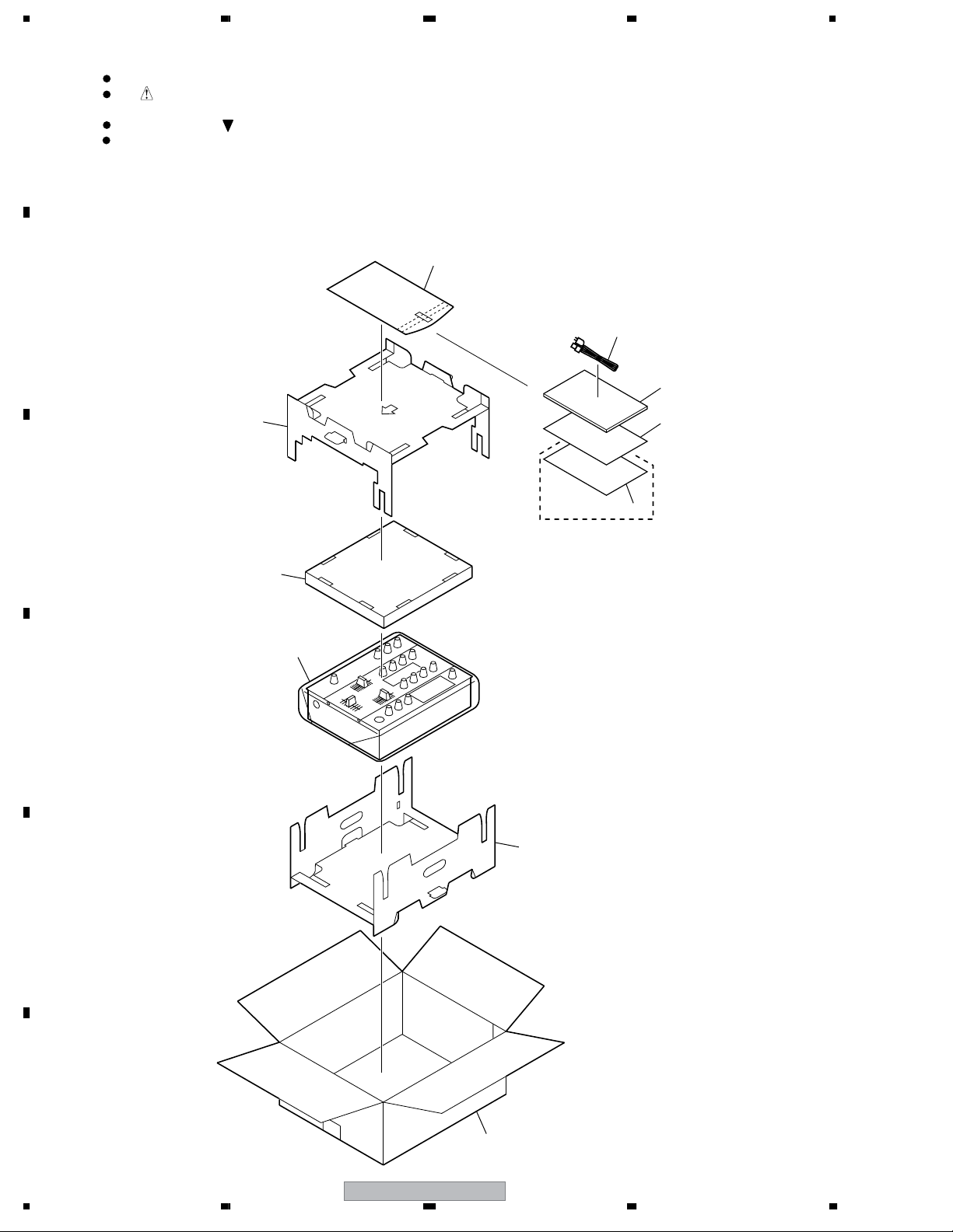
2.1 PACKING SECTION
B
C
10
7
1
2
4
5
KUCXJ only
11
8
D
9
E
F
12
6
1234
DJM-400
>
>
5678
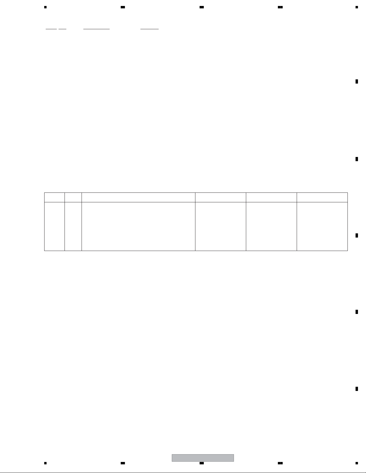
(1) PACKING SECTION PARTS LIST
No. Description Part No.
Mark
1Power Cord See Contrast table (2)
2 Operating Instructions See Contrast table (2)
3• • • • •
NSP 4 User Registration Seat DRM1262
NSP 5 Warranty Card See Contrast table (2)
6• • • • •
NSP 7 Polyethylene Bag AHG7117
(0.06 x 230 x 340)
8Packing Sheet AHG7015
9Pad A DHA1706
A
10 Pad B DHA1707
11 Pad C DHA1713
12 Packing Case See Contrast table (2)
(2) CONTRAST TABLE
DJM-400/KUCXJ, RLXJ and WYXJ5 are constructed the same except for the following:
Mark No. Symbol and Description DRM-400/KUCXJ DRM-400/RLXJ DRM-400/WYXJ5
1Power Cord ADG7021 ADG1154 ADG1154
2 Operating Instructions (English) DRB1405 Not used Not used
2 Operating Instructions (English/ Spanish/ Chinese) Not used DRB1406 Not used
2 Operating Instructins
(English/ French/ German/ Italian/ Duch/ Spanish)
NSP 5 Warranty Card ARY7043 Not used Not used
12 Packing Case DHG2605 DHG2606 DHG2604
Not used Not used DRB1404
B
C
D
56
DJM-400
E
F
7
7
8
1234
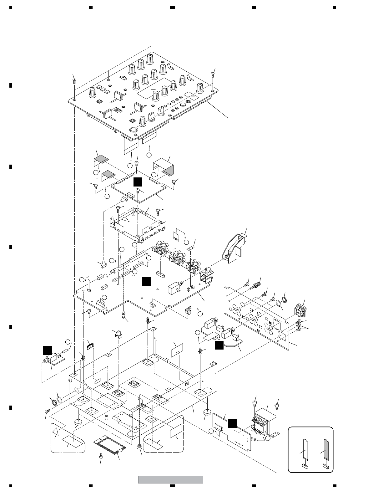
2.2 EXTERIOR SECTION
A
31
B
10
F
11
35
E
C
12
E
35
I
H
A
35
33
H
18
I
G
9
G
35
1
33
6
D
31
Refer to
"2.3 CONTROL PANEL SECTION".
15
F
A
D
B
35
14
25
A
37
23
17
35
19
C
E
4
26
27
31
36
F
KUCXJ only RLXJ only
8
1234
20
13
B
17
39
DJM-400
16
38
22
2
C
D
D
17
5
23
B
I
8
35
34
27
35
24
26
34
35
21
3
32
32
7
C
NON-CONTACT
NON-CONTACT
SIDE
SIDE
CONTACT SIDE
CONTACT SIDE
>
>
5678
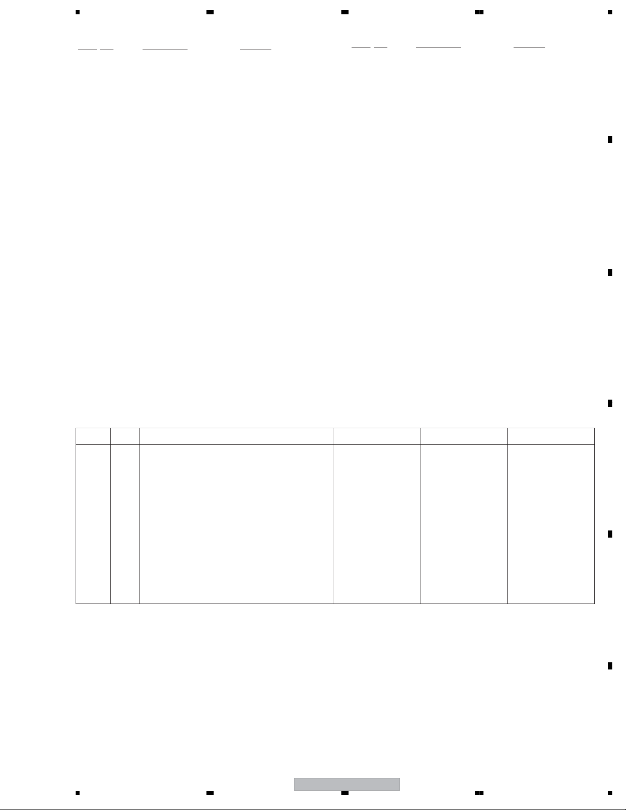
(1) EXTERIOR SECTION PARTS LIST
No. Description Part No.
Mark
1 MAIN Assy DWX2527
2JACK Assy See Contrast table (2)
3 MIC Assy DWX2517
4 HP Assy DWX2518
5 TRANS Assy See Contrast table (2)
6 Fuse (FU1 : T250mA) AEK1048
7Power Transformer See Contrast table (2)
8 Earth Terminal AKE-031
9 26P Flexible Cable DDD1306
10 22P Flexible Cable DDD1307
11 19P Flexible Cable DDD1308
12 Small Connector PF07PP-R12
NSP 13 Spacer AEB7092
14 PCB Mold AMR2534
15 Power Knob DAC2339
16 Blind Sheet DEC2907
17 PCB Spacer DEC2942
18 PCB Stay DNF1739
19 ICP Cover DNK4625
NSP 20 Card Spacer REC1156
No. Description Part No.
Mark
NSP 21 Rear Panel See Contrast table (2)
22 Chassis Assy See Contrast table (2)
23 Insulator DEB1795
24 Power Knob Guide DNK4198
25 Blind Cap DNK4218
26 Phone Washer DEC2920
27 Nut M12 NKX2FNI
28 • • • • •
29 • • • • •
30 • • • • •
31 Screw 3x8 DBA1290
32 Screw BBZ40P060FTC
33 Screw BBZ30P140FTC
34 Screw BPZ30P080FTB
35 Screw BBZ30P060FTB
36 Label See Contrast table (2)
37 FCC.Class B Label See Contrast table (2)
38 V Select Label See Contrast table (2)
39 FCC Label See Contrast table (2)
A
B
C
(2) CONTRAST TABLE
DJM-400/KUCXJ, RLXJ and WYXJ5 are constructed the same except for the following:
Mark No. Symbol and Description DRM-400/KUCXJ DRM-400/RLXJ DRM-400/WYXJ5
2JACK Assy DWX2524 DWX2525 DWX2516
5 TRANS Assy DWX2519 DWX2526 DWX2519
>
NSP 21 Rear Panel (KUC) DNC1784 Not used Not used
NSP 21 Rear Panel (RL) Not used DNC1805 Not used
NSP 21 Rear Panel (WY) Not used Not used DNC1787
NSP 36 Label DRW1975 Not used Not used
NSP 37 FCC.Class B Label DRW2300 Not used Not used
7Power Transformer DTT1201 DTT1202 DTT1202
22 Chassis Assy DXB1890 DXB1891 DXB1890
38 V Select Label Not used DRW2298 Not used
39 FCC Label Not used DRW2299 Not used
D
E
56
DJM-400
F
9
7
8
1234
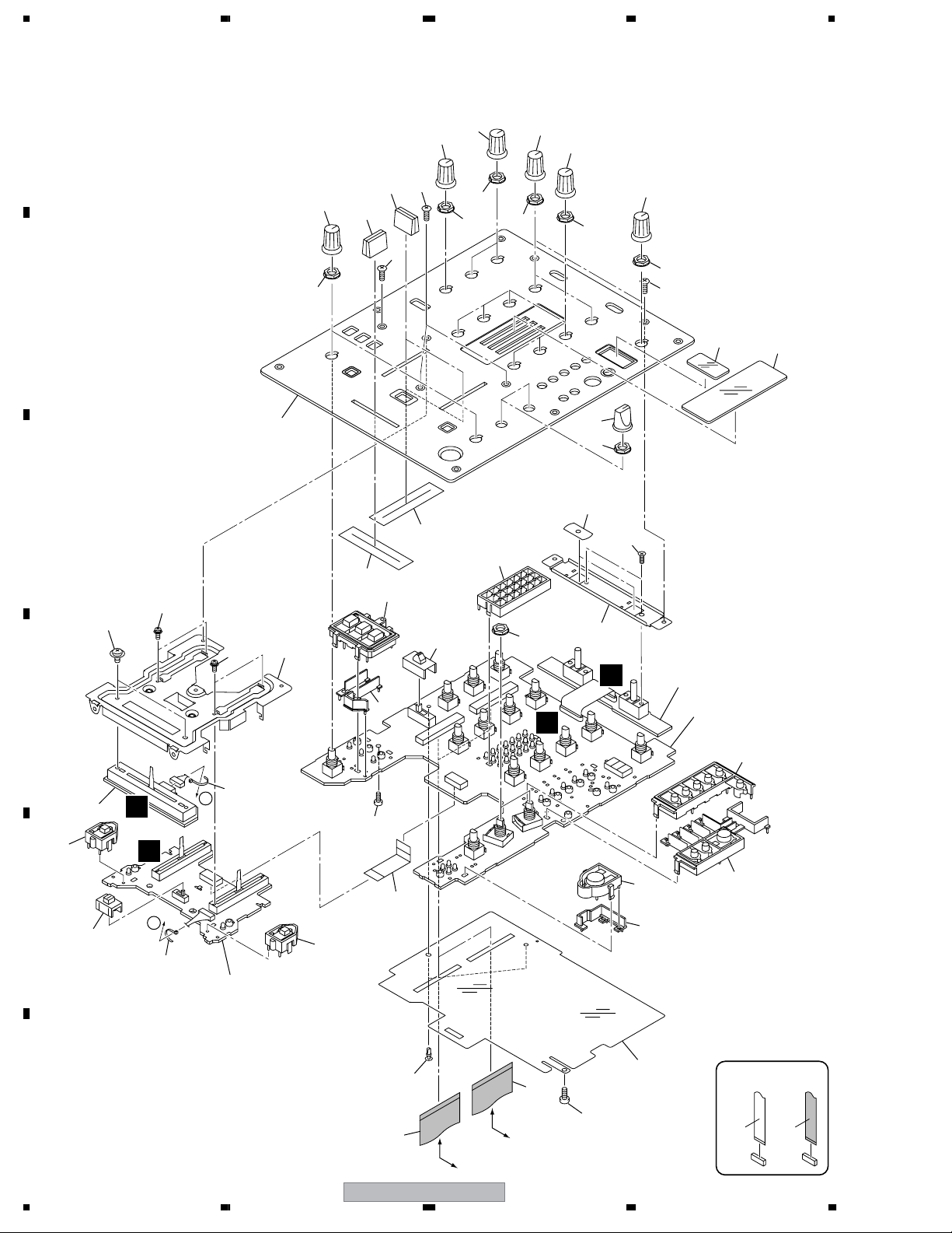
2.3 CONTROL PANEL SECTION
A
31
24
14
24
31
29
B
13
C
8
18
33
36
36
35
15
14
29
29
8
21
10
29
29
15
14
16
7
29
29
34
F
37
14
29
31
26
3
25
D
27
4
H
19
E
20
F
G
A
A
19
27
2
10
1234
11
32
6
28
5
DJM-400
E
23
12
9
5
32
JACK CN502
JACK CN500
1
17
NON-CONTACT
22
SIDE
CONTACT SIDE

5678
(1) CONTROL PANEL SECTION PARTS LIST
Mark No. Description Part No.
1 VRSW Assy DWX2520
2FADER Assy DWX2521
3 CHRV Assy DWX2522
4 CFVR Assy DWX2523
5 36P Flexible Cable DDD1305
6 12P Flexible Cable DDD1310
7 SW Packing (B) DEC2574
8Fader Packing DEC2903
9 Insulation Sheet DEC2940
10 Level Meter Holder DNK4622
A
11 Blind Plate CUE DNK4624
12 Blind Plate EFFECT DNK4654
13 Control Panel DNB1138
14 Rotary VR Knob (B) DAA1183
15 Rotary VR Knob (G) DAA1184
16 Rotary SW Knob DAA1185
17 Button TAP DAC2341
18 Button CUE DAC2343
19 Button FADER DAC2344
20 SW Cap FADER DAC2345
21 SW Cap MIC DAC2346
22 Button BEAT DAC2369
23 Button EFFECT DAC2370
24 Slider Knob (L2) DAC2371
25 Level Plate DAH2445
26 7seg Plate DAH2446
27 Binder (SKB-909BK) ZCA-SKB90BK
28 Nyron Rivet 3x4.5 RBM-003
29 Nut M9 DBN1008
30 • • • • •
B
C
D
31 Screw 3x8 DBA1290
32 Screw BPZ26P080FTC
33 Screw AMZ30P040FTC
34 Lever SW Stay DNF1740
35 Fader Stay DNF1746
36 Screw PMH20P040FTC
37 Screw CMZ26P050FTB
56
DJM-400
E
F
11
7
8
1234
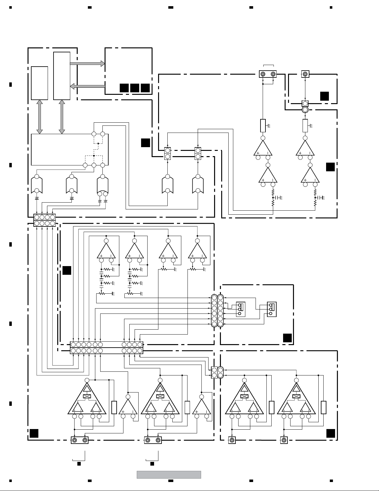
3. BLOCK DIAGRAM AND SCHEMATIC DIAGRAM
3.1 BLOCK DIAGRAM
3.1.1 OVERALL BLOCK DIAGRAM
A
LED 7seg
7seg (×3)
LED (36th)
CPU
IC700
IC709
SDRAM 64M
K4S641632H-TC75-K
DYW1755
VR, SW (32th)
(32th)
KEY, SW
VRSW ASSY
FADER ASSY
CFVR ASSY
E
G
H
JA510
MASTER
1
OUT
2
PHONES
JA2000
CN2000J501
33
C
HP ASSY
IC711
2 12
CN703 (1/2)
262218
262218
CN503 (1/2)
Serial
(500 µsec)
communication
ADC (CH-1)
PCM1803DB
16
16
14
DSP
IC708
D607A003BRFP200
91
92
IC712
2 12
2
ADC (CH-2)
PCM1803DB
BA4560F
IC901 (1/2)
VRSW ASSY
18
94
12
3
IC713
1
1
2
PCM1803DB
ADC (MIC/AUX)
BA4560F
IC902 (1/2)
3
MAIN ASSY
A
IC714
1
2
8
8
(2/2)
CN703
2 8
PCM1742KE
DAC (MASTER)
1
BA4560F
IC903 (1/2)
3
CN503
(2/2)
2
CN511
CN702
IC715
PCM1742KE
DAC (PHONES)
BA4560F
IC903 (2/2)
5
Mute
7
1
19
2 8
7
6
IC507 (1/2)
5
NJM4580MD
IC506 (1/2)
NJM4580MD
6
7
5
6
IC509 (2/2)
3
NJM4556AD
IC508 (2/2)
NJM4558F-HT
Mute
1
3
2
1
JACK ASSY (2/2)
B
2
B
C
E
D
Trim
Trim
12
12
6
6
S1201
7 9 1 3
S1202
CHRV ASSY
J1201
5
7
31
35
11
15
5
7
31
35
11
15
E
CN502 CN901
IC502
NJM2121M
2
ch-A
5
ch-B
3
7
6
RIAA
23
23
IC500
BA4560F
3
27
27
19 19
17 17
J801
8 6
1
BA4560F
3
2
8 6 7 9 1 3
CN507 J901
IC800
NJM2121M
ch-A
2
5
ch-B
3
7
6
5
IC504
1
NJM2121M
ch-A
2
2
ch-B
3
7
6
IC501
RIAA
JACK ASSY (1/2)
B
F
12
1234
JA508
PHONO
/LINE
1
CD
JA509
PHONO
CD
/LINE
2
DJM-400
JA800
MIC1/AUX (L)
40 dB
JA801
F
IC801
NJM2121M
ch-A
2
3
MIC2/AUX (R)
5
ch-B
7
40 dB
6
MIC ASSY
D
5678
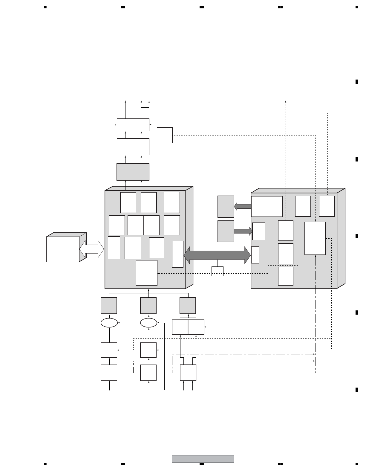
3.1.2 CPU & DSP BLOCK DIAGRAM
A
SDRAM
Talk over
Effect
DSP
PHONES
MUTE
LPF
DAC
switch
Cross fader
processing
processing
MASTER OUT 1
MUTE
LPF
DAC
processing
Isolator
processing
Fader
processing
MASTER OUT 2
MONO/
switch
processing
HP/STEREO
EQ, VR
processing
detection
Level meter
processing
Input, Mute
SW
STEREO
MONO/
STEREO
BPM
detection
switch
interface
Microcomputer
/LED/7seg
Level meter
KEY, VR
(500µsec)
Serial communication
processing
Level meter
Display,
Operation
Serial I/F
CPU
LED/7seg
processing
Fader start
BPM
DSP
CONTROL
processing
Calculation
Registration
firmware
processing
Effect mode
Switching
processing,
B
C
Preference
processing
Noise counterplan
D
ADC
SW
Amp.
Buffer
SW
/LINE
PHONO
PHONO1/LINE1
CD1
ADC
SW
Amp.
Buffer
SW
/LINE
PHONO
PHONO2/LINE2
CD2
ADC
Amp.
Buffer
MIC/AUX
MIC1/AUX_L
Amp.
Buffer
SW
MIC2/AUX_R
/IN-LOOP SAMPER infomation
CPU→DSP : KEY/VR/EFFECT
DSP→CPU : BPW/Level meter
DJM-400
56
E
F
13
7
8
1234
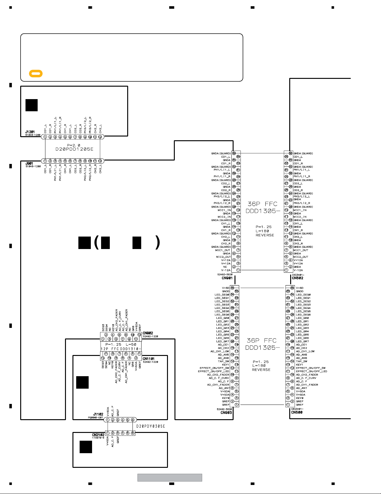
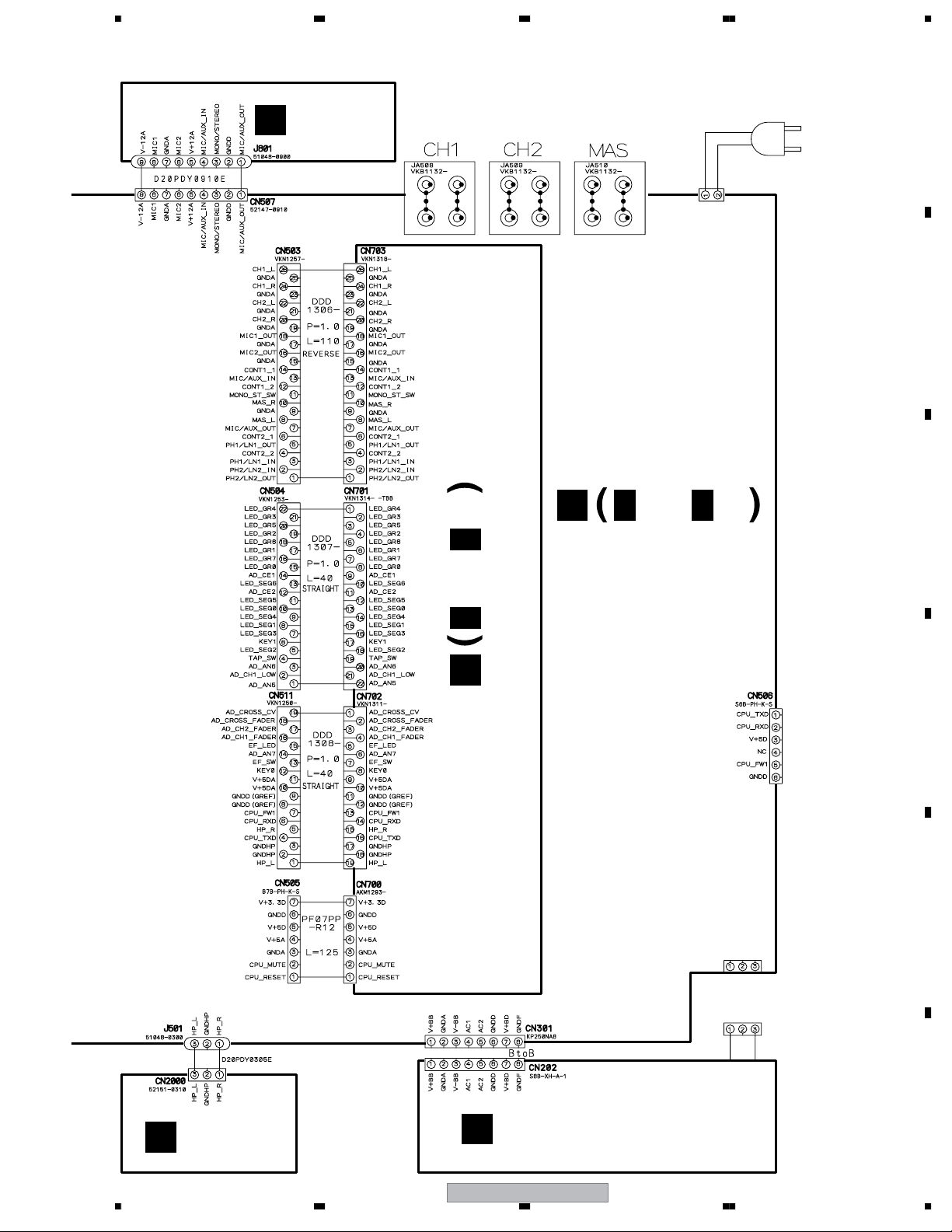
3.2 OVERALL WIRING DIAGRAM
÷
A
B
When ordering service parts, be sure to refer to "EXPLODED VIEWS and PARTS
LIST" or "PCB PARTS LIST".
÷
The > mark found on some component parts indicates the importance of the safety
factor of the part. Therefore, when replacing, be sure to use parts of identical
designation.
÷
: The power supply is shown with the marked box.
CHRV ASSY (DWX2522)
F
C
E
E 1/3 - E 3/3
VRSW ASSY (DWX2520)
D
E
G
FADER ASSY (DWX2521)
F
H
CFVR ASSY (DWX2523)
14
1234
DJM-400
5678
MIC ASSY
D
(DWX2517)
A 1/3 - A 3/3
AN101
KUCXJ : XKP3042
RLXJ, WYXJ5 : XKP3041
B
B 1/4 - B 4/4
JACK ASSY
(KUCXJ : DWX2524)
(RLXJ : DWX2525)
(WYXJ5 : DWX2516)
KUCXJ : ADG7021
RLXJ, WYXJ5 : ADG1154
A
B
C
HP ASSY
C
(DWX2518)
A
MAIN ASSY (DWX2527)
TRANS ASSY
I
(KUCXJ, WYXJ5 : DWX2519)
(RLXJ : DWX2526)
56
DJM-400
D
E
CN102
RLXJ : B3P5-VH (3P)
KUCXJ, WYXJ5 : B2P3-VH (2P)
J3 (RLXJ) : DKP3745 (3P)
J2 (KUCXJ, WYXJ5) : DKP3744 (2P)
F
15
7
8
1234
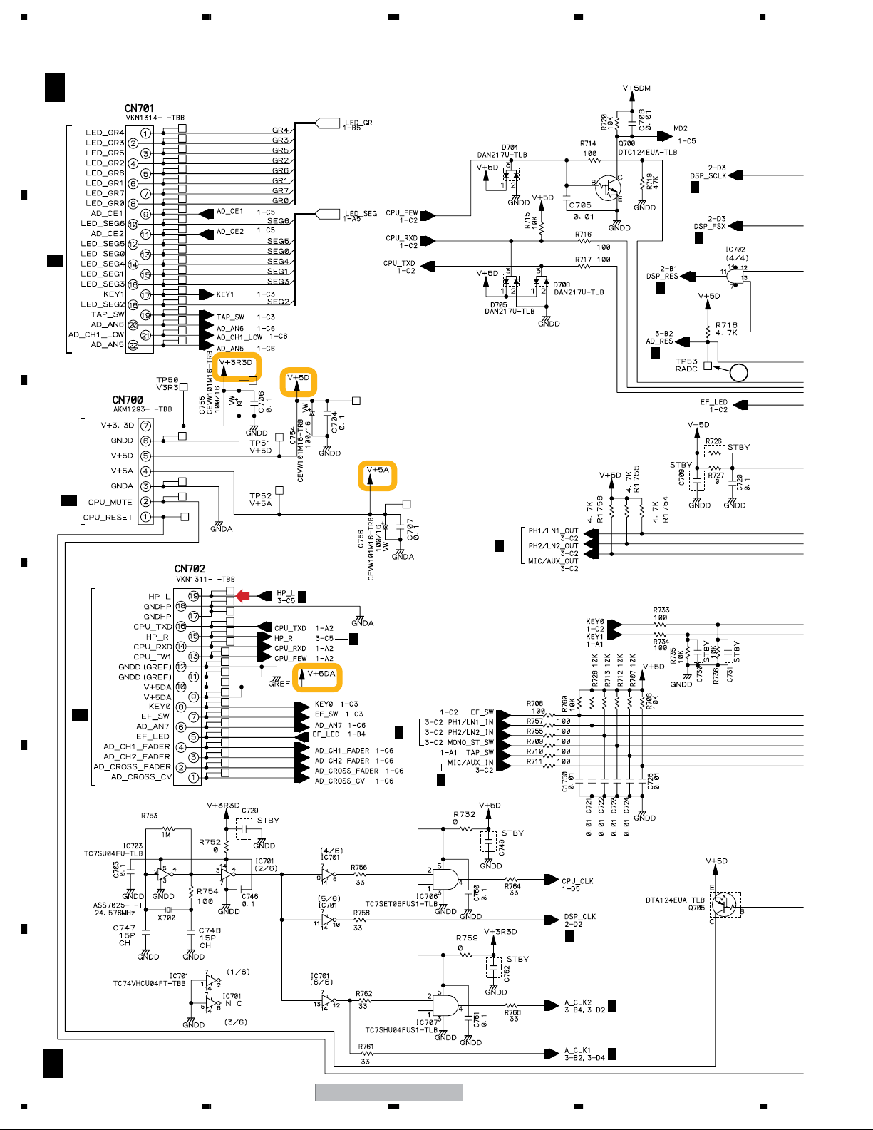
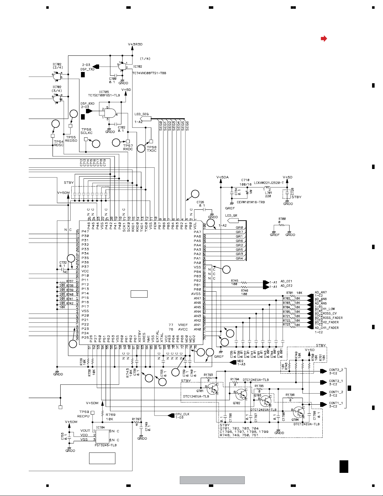
3.3 MAIN ASSY (1/3)
A
B
C
A 1/3
CN504
3/4B
CN505
3/4B
MAIN ASSY (DWX2527)
A 2/3
A 2/3
A 2/3
A 3/3
7
A 3/3
(HP)
D
CN511
A 3/3
A 3/3
3/4B
A 3/3
A 3/3
E
A 2/3
F
16
A 3/3
A 3/3
A 1/3
DJM-400
1234
5678
(HP)
: HP L ch
A
A 2/3
5
A 2/3
6
B
4
3
2
1
C
18
8
IC700
DYW1755
(HD64F3062BFBL25)
CPU
17
D
9
13
14
12
10
11
SYSTEM
RESET
56
DJM-400
15
16
E
A 3/3
F
A 1/3
17
7
8
1234
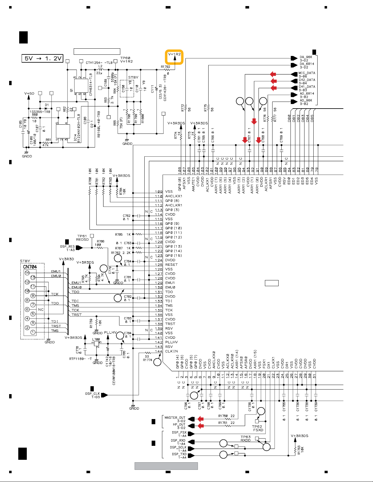
3.4 MAIN ASSY (2/3)
A
B
C
A 2/3
MAIN ASSY (DWX2527)
DC-DC CONVERTER
(MICD)
A 3/3
(MICD)
(CH2D)
(CH1D)
79 8
(CH2D)
(CH1D)
D
E
F
18
A 2/3
A 1/3
10
11
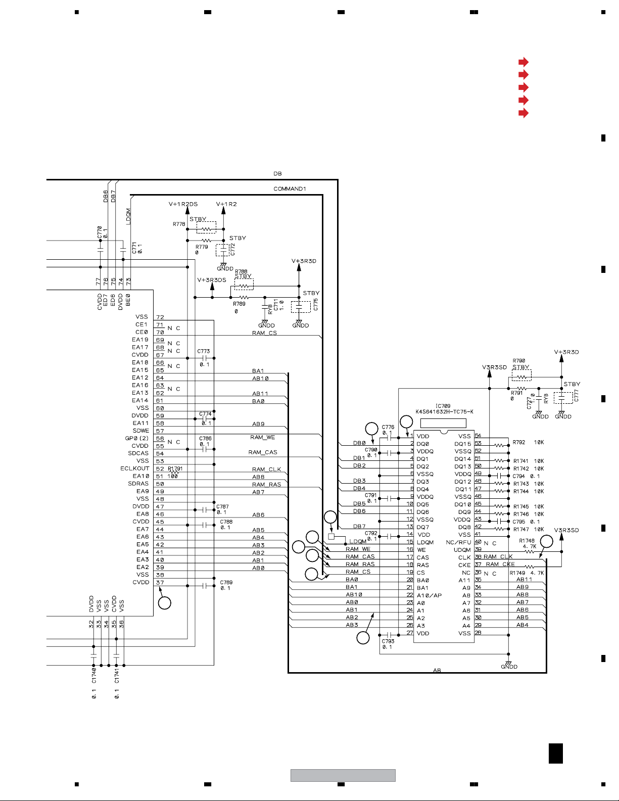
IC708
D607A003BRFP200-K
DSP
12
13
14
A 1/3
1
2
3
A 3/3
A 1/3
(MASTERD)
(HPD)
4
5
DJM-400
1234
5678
(CH1D)
: CH 1 Data
(CH2D)
(MICD)
(MASTERD)
(HPD)
: CH 2 Data
: MIC Data
: MASTER Data
: HP Data
A
B
C
15
16
SDRAM 64M
D
17
18
19
23
20
21
E
6
22
DJM-400
56
F
A 2/3
19
7
8
1234
3.5 MAIN ASSY (3/3)
A
B
C
A 3/3
MAIN ASSY (DWX2527)
5
A 1/3
(CH1) (CH2)
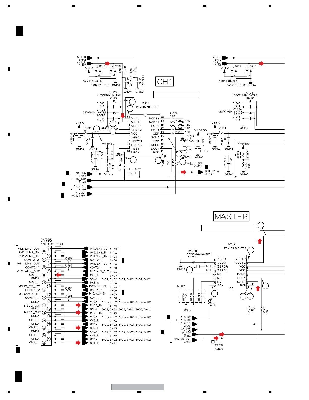
A/D CONVERTER for CH1
2
1
(CH1)
ADC
3
4
9
6
7
(CH1D)
8
A 2/3
A 2/3
A 1/3
D
A 1/3
(MASTER)
D/A CONVERTER for MASTER
DAC
33
31
32
(MASTER)
30
E
(MIC2)
(MIC1)
(CH2)
A 1/3
A 1/3
A 2/3
(MASTERD)
34
(HPD)
28
29
(MASTERD)
F
20
CN503
2/4B
A 3/3
(CH1)
DJM-400
1234
(CH2)
13
11
12
5678
(CH1)
: CH 1 L ch
(CH2)
10
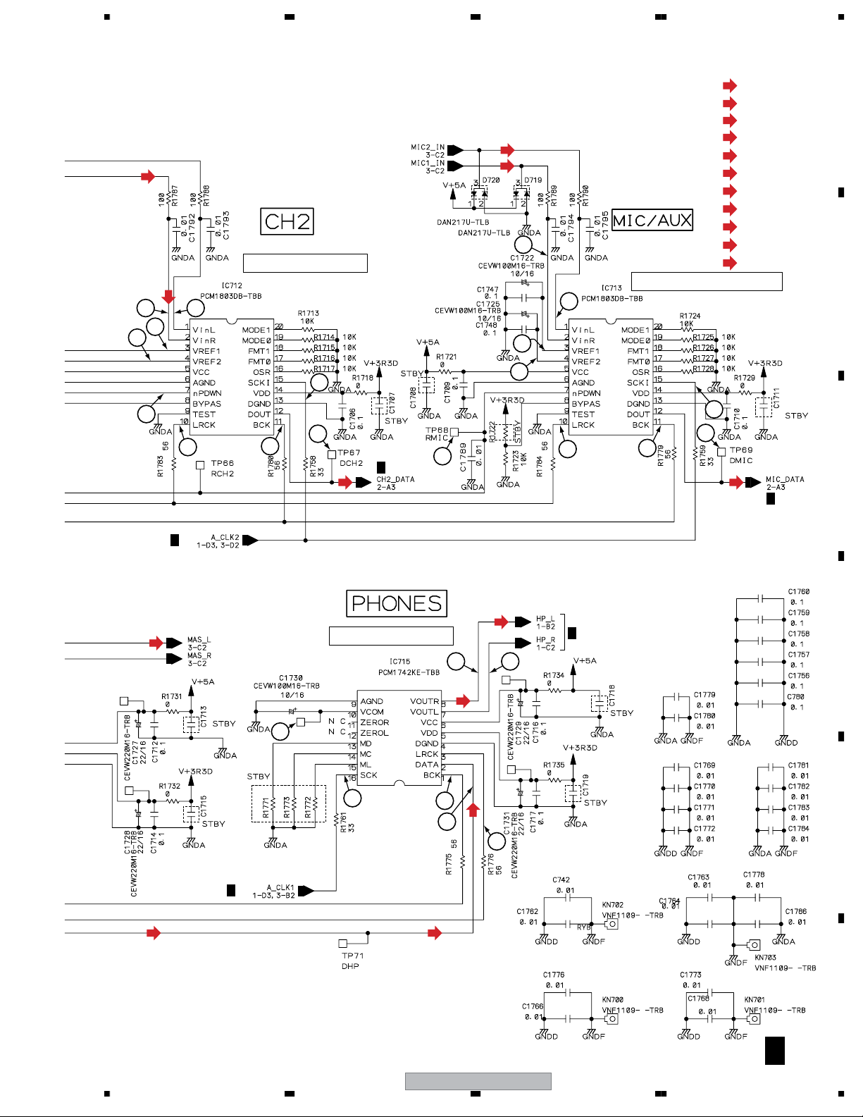
A/D CONVERTER for CH2
ADC
(MIC1)
(MIC2)
20
19
(MASTERD)
(MASTER)
A/D CONVERTER for MIC/AUX
ADC
(CH2)
(MIC1)
(MIC2)
(CH1D)
(CH2D)
(MICD)
(HPD)
(HP)
: CH 2 L ch
: MIC 1 input ch
: MIC 2 input ch
: CH 1 Data
: CH 2 Data
: MIC Data
: MASTER Data
: HP Data
: MASTER L ch
: HP L ch
A
B
22
14
(MASTER)
15
A 1/3
16
40
18
17
A 2/3
(CH2D)
D/A CONVERTER for H.P
DAC
24
(HP)
(HP)
23
27
21
25
A 1/3
26
(MICD)
C
A 2/3
D
3839
41
A 1/3
(HPD) (HPD)
56
35
36
DJM-400
(HPD)
37
E
F
A 3/3
21
7
8
1234
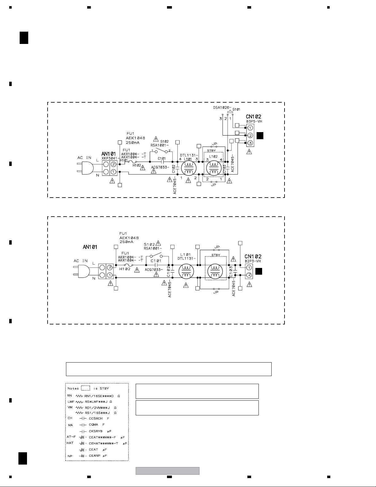
3.6 JACK ASSY (1/4)
A
B
C
B 1/4
JACK ASSY (KUCXJ : DWX2524)
(RLXJ : DWX2525)
(WYXJ5 : DWX2516)
FOR RLXJ
FOR KUCXJ and WYXJ5
J3
I
KUCXJ : XKP3042
WYXJ5 : XKP3041
J2
I
D
E
• NOTE FOR FUSE REPLACEMENT
CAUTION -
FOR CONTINUED PROTECTION AGAINST RISK OF FIRE.
REPLACE WITH SAME TYPE AND RATINGS ONLY.
CAUTION : FOR CONTINUED PROTECTION AGAINST RISK OF FIRE.
CAUTION : FOR CONTINUED PROTECTION AGAINST RISK OF FIRE.
REPLACE ONLY WITH SAME TYPE NO. 491.250 MFD, BY
LITTELFUSE INK. FOR IC300 to IC302 and IC304.
REPLACE ONLY WITH SAME TYPE NO. 491.400 MFD, BY
LITTELFUSE INK. FOR IC303 and IC308.
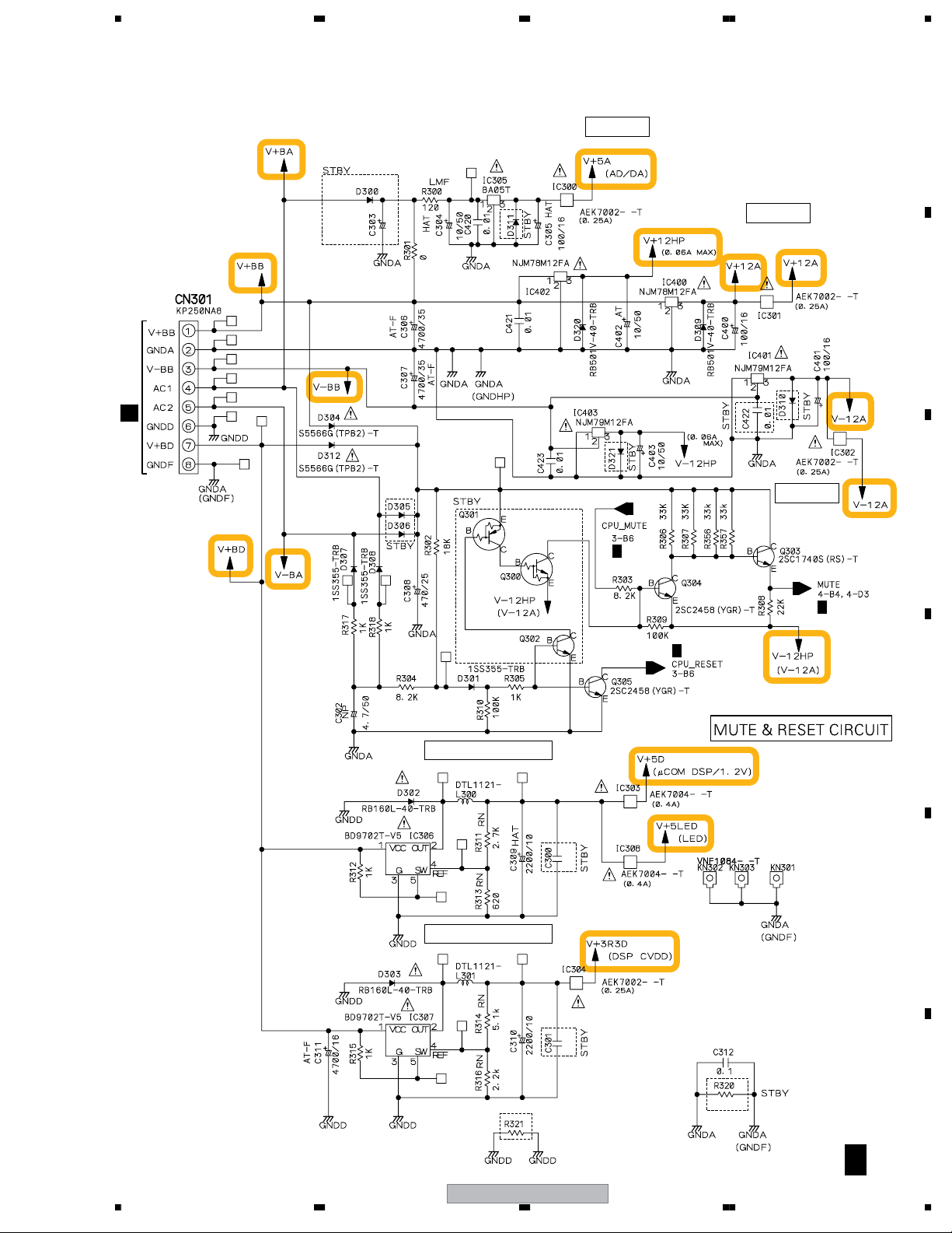
F
22
B 1/4
DJM-400
1234
5678
CN202
I
+5V REG.
A
+12V REG.
B
-12V REG.
C
B 3/4
DC-DC CONVERTER
DC-DC CONVERTER
B 4/4
B 3/4
D
E
56
DJM-400
F
B 1/4
23
7
8
1234
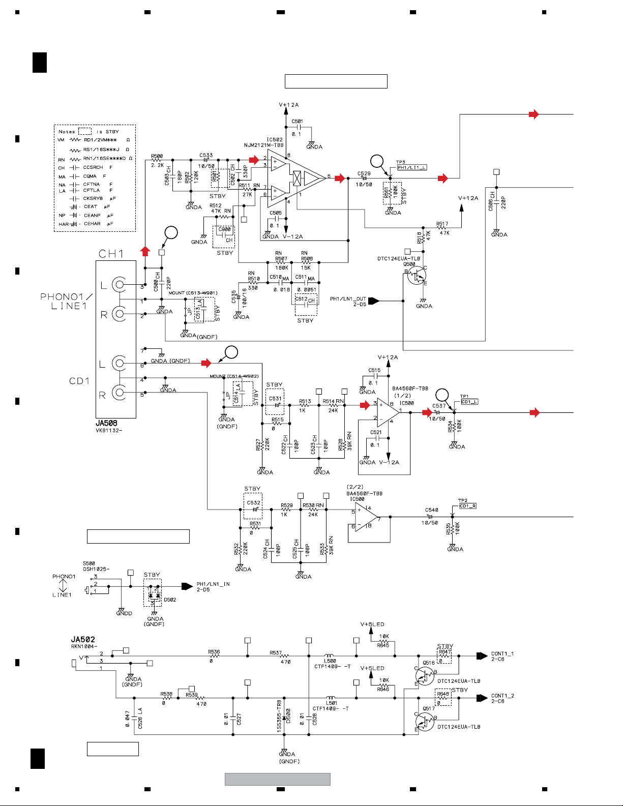
3.7 JACK ASSY (2/4)
A
B
C
B 2/4
JACK ASSY (KUCXJ : DWX2524)
(RLXJ : DWX2525)
(WYXJ5 : DWX2516)
(PL1)
2
(PL1)
(CD1)
1
PHONO/LINE SELECT AMP
(PL1)
4
(PL1) (PL1)
(CD1)
D
PHONO1/LINE1 SELECT
E
3
(CD1)
(CD1)
F
24
CONTROL1
B 2/4
DJM-400
1234
5678
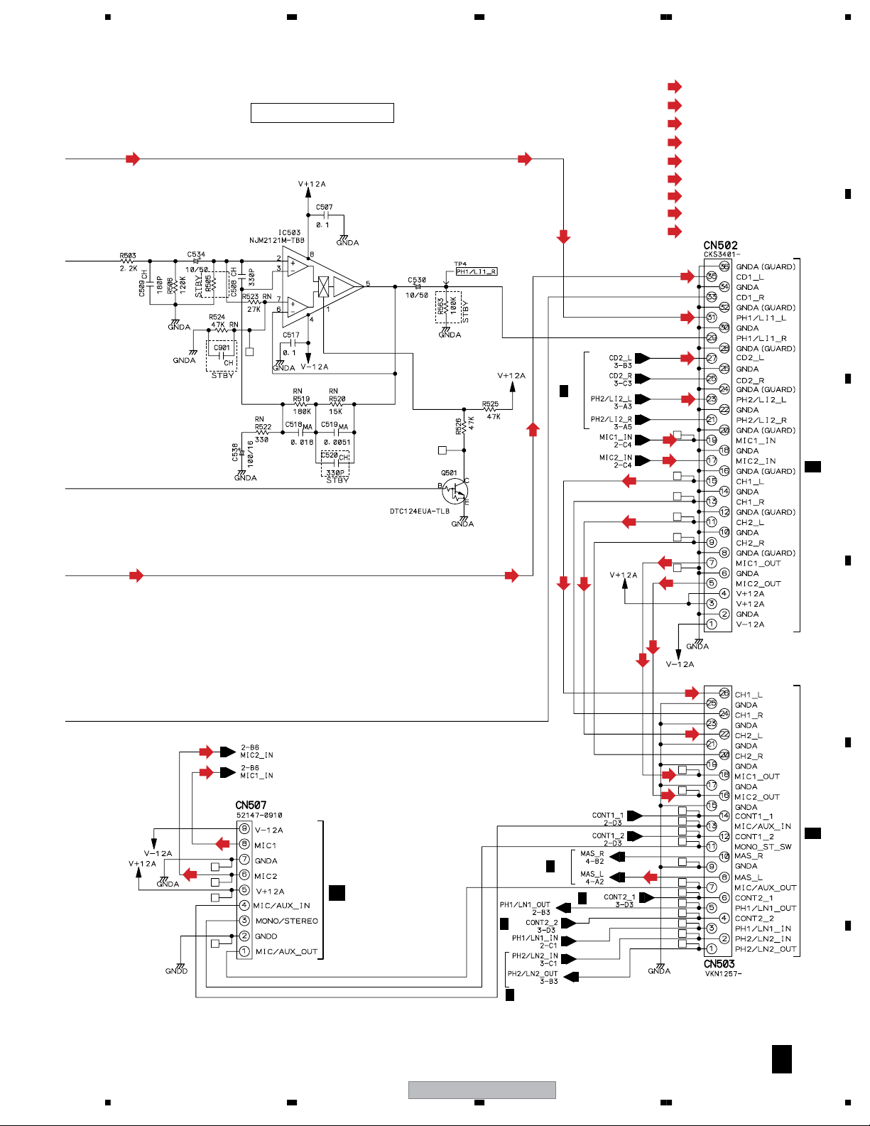
PHONO/LINE SELECT AMP
(PL1) (PL1)
(PL1)
(PL1)
(PL2)
(CD1)
(CD2)
(CH1)
(CH2)
(MIC1)
(MIC2)
(MASTER)
: PHONO 1/LINE 1 input L ch
: PHONO 2/LINE 2 input L ch
: CD 1 input L ch
: CD 2 input L ch
: CH 1 L ch
: CH 2 L ch
: MIC 1 input ch
: MIC 2 input ch
: MASTER L ch
(CD1)
(PL1)
(CD2)
A
B
(CD1) (CD1)
(MIC2)
(MIC1)
(MIC1)
(CD1)
B 3/4
(CH1)
(CH2)
(CH1)
(CH2)
(MIC1)
(MIC1)
(MIC2)
(PL2)
(MIC1)
(MIC2)
(MIC2)
(CH1)
(CH2)
(MIC1)
(MIC2)
CN901
1/3E
C
D
CN703
3/3A
E
(MIC2)
J801
D
B 3/4
B 3/4
DJM-400
56
B 4/4
7
(MASTER)
B 3/4
F
B 2/4
25
8
1234
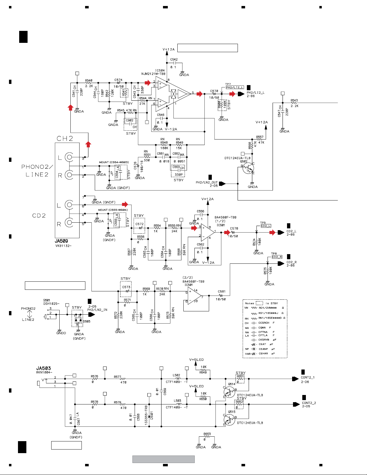
3.8 JACK ASSY (3/4)
A
B
C
B 3/4
JACK ASSY (KUCXJ : DWX2524)
(RLXJ : DWX2525)
(WYXJ5 : DWX2516)
(PL2)
(PL2)
(PL2)
(CD2)
PHONO/LINE SELECT AMP
(PL2)
(PL2)
B 2/4
B 2/4
(CD2)
D
PHONO2/LINE2 SELECT
B 2/4
E
(CD2)
(CD2)
B 2/4
B 2/4
B 2/4
B 2/4
F
26
B 3/4
CONTROL2
DJM-400
1234
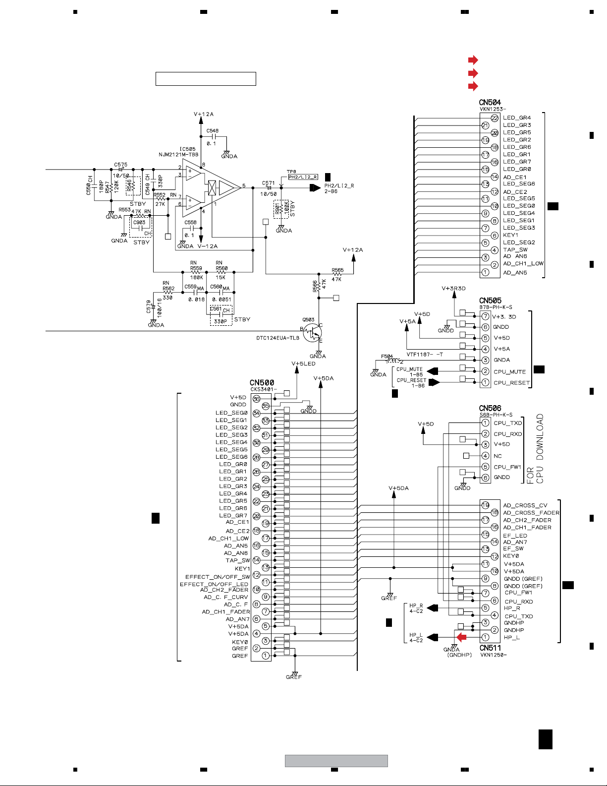
5678
(PL2)
: PHONO 2/LINE 2 input L ch
PHONO/LINE SELECT AMP
(CD2)
(HP)
: CD 2 input L ch
: HP L ch
A
B 2/4
B 1/4
CN701
1/3A
CN700
1/3A
B
C
D
3/3E
CN903
B 4/4
DJM-400
56
CN702
1/3A
E
(HP)
F
B 3/4
27
7
8
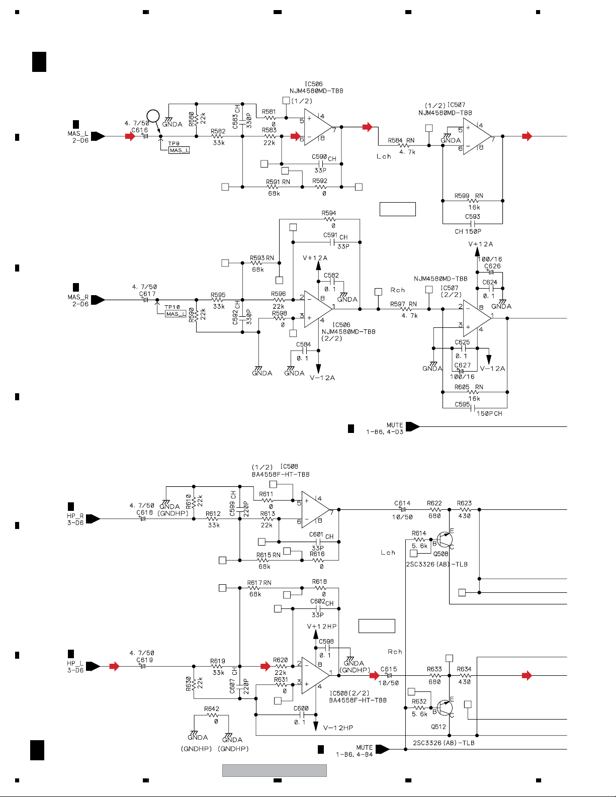
1234
3.9 JACK (4/4) and HP ASSYS
A
B
C
B 4/4
JACK ASSY (KUCXJ : DWX2524)
(RLXJ : DWX2525)
(WYXJ5 : DWX2516)
B 2/4
B 2/4
(MASTER)
5
(MASTER)
(MASTER)
(MASTER)
FILTER
B 1/4
D
B 3/4
E
FILTER
B 3/4
F
(HP) (HP)
(HP)
(HP)
B 4/4
28
B 1/4
DJM-400
1234
 Loading...