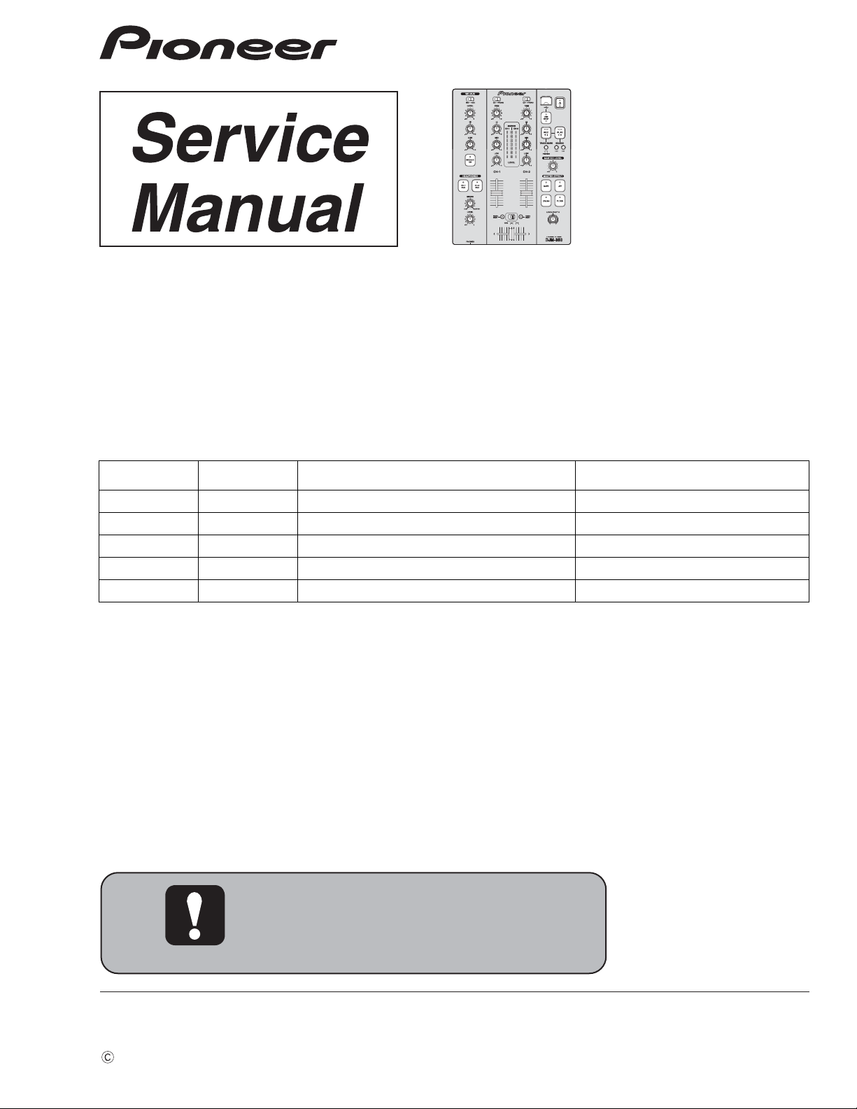
Pioneer DJM-350 Service manual
2010
DJM-350
For details, refer to "Important Check Points for good servicing".
DJ MIXER
DJM-350
THIS MANUAL IS APPLICABLE TO THE FOLLOWING MODEL(S) AND TYPE(S).
Model Type Power Requirement Remarks
DJM-350 SYXJ8 AC 220 V to 240 V
DJM-350 CUXJ AC 120 V
DJM-350 LXJ AC 110 V to 120 V or 220 V to 240 V
DJM-350 KXJ5 AC 220 V
DJM-350 AXJ5 AC 220 V to 240 V
ORDER NO.
RRV4063
PIONEER CORPORATION 1-1, Shin-ogura, Saiwai-ku, Kawasaki-shi, Kanagawa 212-0031, Japan
PIONEER ELECTRONICS (USA) INC. P.O. Box 1760, Long Beach, CA 90801-1760, U.S.A.
PIONEER EUROPE NV Haven 1087, Keetberglaan 1, 9120 Melsele, Belgium
PIONEER ELECTRONICS ASIACENTRE PTE. LTD. 253 Alexandra Road, #04-01, Singapore 159936
PIONEER CORPORATION
K-IZV MAY
2010 Printed in Japan
1
1. SAFETY PRECAUTIONS
The following check should be performed for the
continued protection of the customer and service
technician.
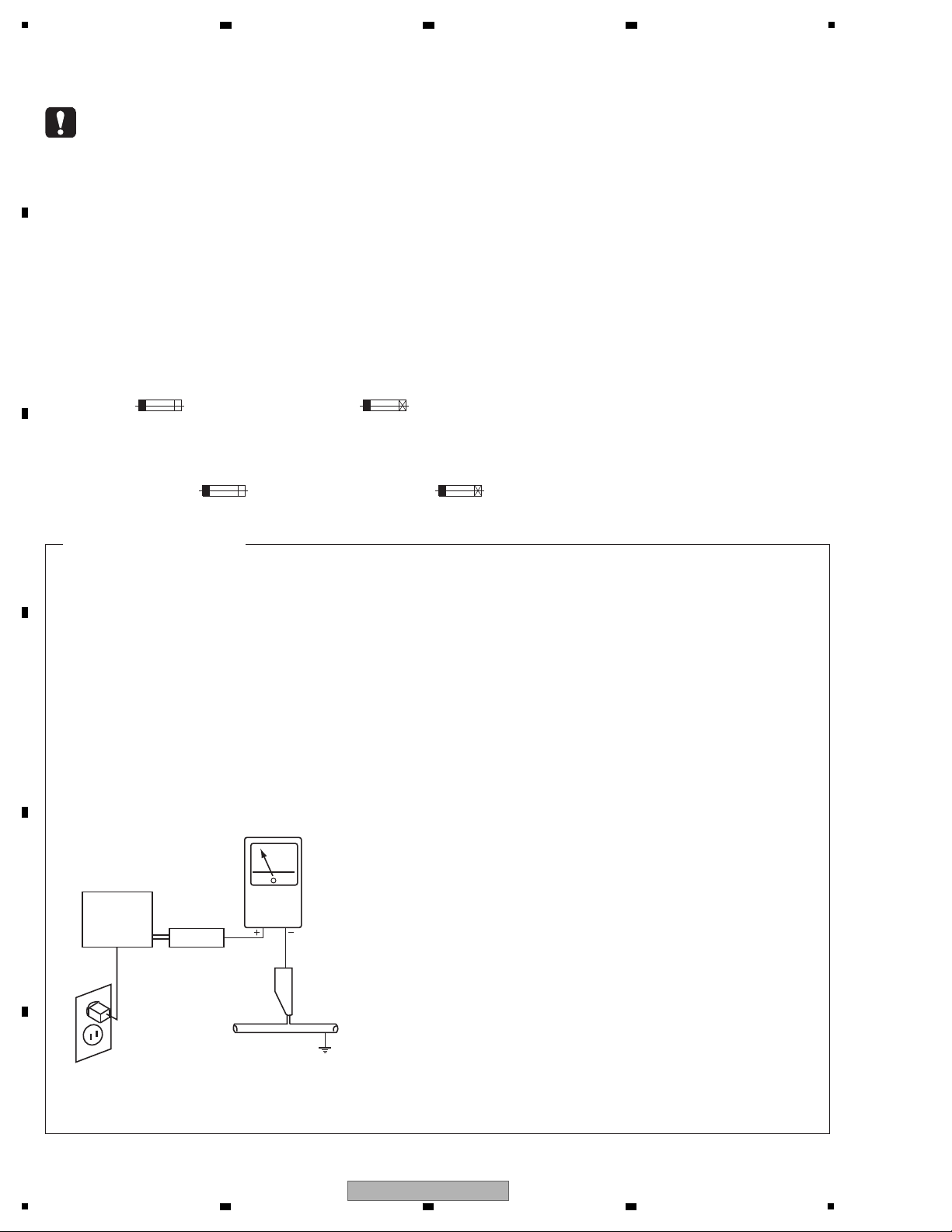
LEAKAGE CURRENT CHECK
Measure leakage current to a known earth ground
(water pipe, conduit, etc.) by connecting a leakage
current tester such as Simpson Model 229-2 or
equivalent between the earth ground and all exposed
metal parts of the appliance (input/output terminals,
screwheads, metal overlays, control shaft, etc.). Plug
the AC line cord of the appliance directly into a 120V
AC 60 Hz outlet and turn the AC power switch on. Any
current measured must not exceed 0.5 mA.
ANY MEASUREMENTS NOT WITHIN THE LIMITS
OUTLINED ABOVE ARE INDICATIVE OF A POTENTIAL
SHOCK HAZARD AND MUST BE CORRECTED BEFORE
RETURNING THE APPLIANCE TO THE CUSTOMER.
2. PRODUCT SAFETY NOTICE
Many electrical and mechanical parts in the appliance
have special safety related characteristics. These are
often not evident from visual inspection nor the protection
afforded by them necessarily can be obtained by using
replacement components rated for voltage, wattage, etc.
Replacement parts which have these special safety
characteristics are identified in this Service Manual.
Electrical components having such features are
identified by marking with a > on the schematics and on
the parts list in this Service Manual.
The use of a substitute replacement component which
does not have the same safety characteristics as the
PIONEER recommended replacement one, shown in the
parts list in this Service Manual, may create shock, fire,
or other hazards.
Product Safety is continuously under review and new
instructions are issued from time to time. For the latest
information, always consult the current PIONEER Service
Manual. A subscription to, or additional copies of,
PIONEER Service Manual may be obtained at a nominal
charge from PIONEER.
Leakage
current
tester
Reading should
not be above
0.5 mA
Device
under
test
Test all
exposed metal
surfaces
Also test with
plug reversed
(Using AC adapter
plug as required)
Earth
ground
AC Leakage Test
(FOR USA MODEL ONLY)
WARNING
This product may contain a chemical known to the State of California to cause cancer, or birth defects or other reproductive
harm.
Health & Safety Code Section 25249.6 - Proposition 65
NOTICE
(FOR CANADIAN MODEL ONLY )
Fuse symbols (fast operating fuse) and/or (slow operating fuse) on PCB indicate that replacement parts must
be of identical designation.
REMARQUE
(POUR MODÈLE CANADIEN SEULEMENT)
Les symboles de fusible (fusible de type rapide) et/ou (fusible de type lent) sur CCI indiquent que les pièces
de remplacement doivent avoir la même désignation.
This service manual is intended for qualified service technicians ; it is not meant for the casual do-ityourselfer. Qualified technicians have the necessary test equipment and tools, and have been trained
to properly and safely repair complex products such as those covered by this manual.
Improperly performed repairs can adversely affect the safety and reliability of the product and may
void the warranty. If you are not qualified to perform the repair of this product properly and safely, you
should not risk trying to do so and refer the repair to a qualified service technician.
2 3 4
SAFETY INFORMATION
A
B
C
D
E
F
2
1
2 3 4
DJM-350
5
[Important Check Points for Good Servicing]
In this manual, procedures that must be performed during repairs are marked with the below symbol.
Please be sure to confirm and follow these procedures.
1. Product safety
Please conform to product regulations (such as safety and radiation regulations), and maintain a safe servicing environment by
following the safety instructions described in this manual.
1 Use specified parts for repair.
Use genuine parts. Be sure to use important parts for safety.
2 Do not perform modifications without proper instructions.
Please follow the specified safety methods when modification(addition/change of parts) is required due to interferences such as
radio/TV interference and foreign noise.
3 Make sure the soldering of repaired locations is properly performed.
When you solder while repairing, please be sure that there are no cold solder and other debris.
Soldering should be finished with the proper quantity. (Refer to the example)
4 Make sure the screws are tightly fastened.
Please be sure that all screws are fastened, and that there are no loose screws.
5 Make sure each connectors are correctly inserted.
Please be sure that all connectors are inserted, and that there are no imperfect insertion.
6 Make sure the wiring cables are set to their original state.
Please replace the wiring and cables to the original state after repairs.
In addition, be sure that there are no pinched wires, etc.
7 Make sure screws and soldering scraps do not remain inside the product.
Please check that neither solder debris nor screws remain inside the product.
8 There should be no semi-broken wires, scratches, melting, etc. on the coating of the power cord.
Damaged power cords may lead to fire accidents, so please be sure that there are no damages.
If you find a damaged power cord, please exchange it with a suitable one.
9 There should be no spark traces or similar marks on the power plug.
When spark traces or similar marks are found on the power supply plug, please check the connection and advise on secure
connections and suitable usage. Please exchange the power cord if necessary.
a Safe environment should be secured during servicing.
When you perform repairs, please pay attention to static electricity, furniture, household articles, etc. in order to prevent injuries.
Please pay attention to your surroundings and repair safely.
2. Adjustments
To keep the original performance of the products, optimum adjustments and confirmation of characteristics within specification.
Adjustments should be performed in accordance with the procedures/instructions described in this manual.
4. Cleaning
For parts that require cleaning, such as optical pickups, tape deck heads, lenses and mirrors used in projection monitors, proper
cleaning should be performed to restore their performances.
3. Lubricants, Glues, and Replacement parts
Use grease and adhesives that are equal to the specified substance.
Make sure the proper amount is applied.
5. Shipping mode and Shipping screws
To protect products from damages or failures during transit, the shipping mode should be set or the shipping screws should be
installed before shipment. Please be sure to follow this method especially if it is specified in this manual.
6 7 8
A
B
C
D
5
DJM-350
6 7 8
E
F
3

1
2 3 4
CONTENTS
SAFETY INFORMATION ..........................................................................................................................................................2
1. SERVICE PRECAUTIONS ....................................................................................................................................................5
A
B
C
D
E
1.1 NOTES ON SOLDERING ...............................................................................................................................................5
1.2 FOR VOLTAGE MONITORING .......................................................................................................................................6
2. SPECIFICATIONS .................................................................................................................................................................7
2.1 SPECIFICATIONS...........................................................................................................................................................7
2.2 PANEL FACILITIES .........................................................................................................................................................8
3. BASIC ITEMS FOR SERVICE.............................................................................................................................................10
3.1 CHECK POINTS AFTER SERVICING..........................................................................................................................10
3.2 PCB LOCATIONS .........................................................................................................................................................11
4. BLOCK DIAGRAM...............................................................................................................................................................12
4.1 OVERALL WIRING DIAGRAM......................................................................................................................................12
4.2 OVERALL BLOCK DIAGRAM.......................................................................................................................................14
4.3 POWER BLOCK DIAGRAM..........................................................................................................................................16
5. DIAGNOSIS.........................................................................................................................................................................17
5.1 POWER ON SEQUENCE.............................................................................................................................................17
5.2 TROUBLESHOOTING ..................................................................................................................................................19
5.3 ERROR INDICATION....................................................................................................................................................25
5.4 OPERATION CHECK OF RECORDING / PLAYING / TO FROM A USB DEVICE.......................................................26
6. SERVICE MODE .................................................................................................................................................................27
6.1 TEST MODE .................................................................................................................................................................27
6.2 TEST MODE 2 (REFERENCE INFORMATION)...........................................................................................................32
7. DISASSEMBLY....................................................................................................................................................................33
8. EACH SETTING AND ADJUSTMENT ................................................................................................................................36
8.1 NECESSARY ITEMS TO BE NOTED ...........................................................................................................................36
8.3 USER SETABLE ITEMS ...............................................................................................................................................38
8.4 LIST OF
DEVICES WHOSE OPERATION HAS BEEN CONFIRMED .........................................................................39
9. EXPLODED VIEWS AND PARTS LIST...............................................................................................................................40
9.1 PACKING SECTION......................................................................................................................................................40
9.2 EXTERIOR SECTION...................................................................................................................................................42
9.3 CONTROL PANEL SECTION .......................................................................................................................................44
10. SCHEMATIC DIAGRAM ....................................................................................................................................................46
10.1 JACK ASSY (1/5)........................................................................................................................................................46
10.2 JACK ASSY (2/5)........................................................................................................................................................48
10.3 JACK ASSY (3/5)........................................................................................................................................................50
10.4 JACK (4/5) and HPJK ASSYS.....................................................................................................................................52
10.5 JACK ASSY (5/5)........................................................................................................................................................54
10.6 VRSW ASSY (1/3) ......................................................................................................................................................56
10.7 VRSW ASSY (2/3) ......................................................................................................................................................58
10.8 VRSW ASSY (3/3) ......................................................................................................................................................60
10.9 CRFD ASSY................................................................................................................................................................61
10.10 FADR and USJK ASSYS ..........................................................................................................................................62
10.11 MAIN ASSY (1/3) ......................................................................................................................................................64
10.12 MAIN ASSY (2/3) ......................................................................................................................................................70
10.13 MAIN ASSY (3/3) ......................................................................................................................................................72
PCB CONNECTION DIAGRAM ........................................................................................................................................74
11.
11.1 JACK ASSY.................................................................................................................................................................74
11.2 HPJK and VRSW ASSYS ...........................................................................................................................................78
11.3 CRFD, FADR and USJK ASSYS.................................................................................................................................82
11.4 MAIN ASSY.................................................................................................................................................................84
12. PCB PARTS LIST ..............................................................................................................................................................88
F
4
1
2 3 4
DJM-350

5
• For environmental protection, lead-free solder is used on the printed circuit boards mounted in this unit.
Be sure to use lead-free solder and a soldering iron that can meet specifications for use with lead-free solders for repairs
accompanied by reworking of soldering.
• Compared with conventional eutectic solders, lead-free solders have higher melting points, by approximately 40 ºC.
Therefore, for lead-free soldering, the tip temperature of a soldering iron must be set to around 373 ºC in general, although
the temperature depends on the heat capacity of the PC board on which reworking is required and the weight of the tip of
the soldering iron.
Do NOT use a soldering iron whose tip temperature cannot be controlled.
Compared with eutectic solders, lead-free solders have higher bond strengths but slower wetting times and higher melting
temperatures (hard to melt/easy to harden).
The following lead-free solders are available as service parts:
• Parts numbers of lead-free solder:
GYP1006 1.0 in dia.
GYP1007 0.6 in dia.
GYP1008 0.3 in dia.
6 7 8
1. SERVICE PRECAUTIONS
1.1 NOTES ON SOLDERING
A
B
C
D
E
F
DJM-350
5
6 7 8
5

1
This unit always monitors for power failure and will shut itself off immediately after an error is detected. If an error is generated,
the STANDBY LED will flash after the unit shuts itself off, and no key will be operable.
(In a case of power failure, power supply to not all circuits is stopped. The circuits to which the standby transformer supplies
power will be continued to be powered until the power cord is unplugged.)
Repair the unit, according to “5.2 TROUBLESHOOTING.”
2 3 4
1.2 FOR VOLTAGE MONITORING
A
B
C
D
E
F
6
1
2 3 4
DJM-350

5
General
Power requirements........................AC 220 V to 240 V, 50 Hz/ 60 Hz
(SYXJ8, AXJ5)
AC 120 V, 60 Hz (CUXJ)
AC 110 V to 120 V or 220 V to 240 V, 50 Hz/ 60 Hz (LXJ)
AC 220 V, 60 Hz (KXJ5)
Power consumption.....................17 W (SYXJ8, CUXJ, KXJ5, AXJ5)
18 W (LXJ)
Power consumption (standby)...................................................0.4 W
Main unit weight.........................3.2 kg (SYXJ8, CUXJ, KXJ5, AXJ5)
3.3 kg (LXJ)
Max. dimensions...............218 mm (W) × 107 mm (H) × 301 mm (D)
Tolerable operating temperature...............................+5 °C to +35 °C
Tolerable operating humidity..............5 % to 85 % (no condensation)
Audio Section
Sampling rate..........................................................................48 kHz
A/ D, D/ A converter.................................................................24 bits
Frequency characteristic
CD/ LINE/ MIC.....................................................20 Hz to 20 kHz
S/ N ratio (rated output)
CD........................................................................................97 dB
PHONO................................................................................86 dB
MIC......................................................................................80 dB
Total harmonic distortion (LINE — MASTER1).....................0.007 %
Standard input level / Input impedance
CD....................................................................... –12 dBu/ 36 kΩ
PHONO............................................................... –52 dBu/ 47 kΩ
MIC...................................................................... –52 dBu/ 10 kΩ
AUX..................................................................... –12 dBu/ 27 kΩ
Standard output level / Load impedance / Output impedance
MASTER OUT.............................................+2 dBu/ 10 kΩ/ 2.5 Ω
PHONES......................................................+2 dBu/ 32 Ω/ 150 Ω
Rated output level / Load impedance
MASTER OUT..................................................... +18 dBu/ 10 kΩ
Crosstalk (LINE).......................................................................78 dB
Channel equalizer characteristic
HI...............................................................–∞ to + 9 dB (13 kHz)
MID..............................................................–∞ to + 9 dB (1 kHz)
LOW..............................................................–∞ to +9 dB (70 Hz)
MIC/ AUX equalizer characteristics
HI....................................................... –12 dB to +12 dB (10 kHz)
LOW................................................... –12 dB to +12 dB (100 Hz)
Input/ output terminals
CD input terminal
RCA pin jack........................................................................2 sets
PHONO input terminal
RCA pin jack........................................................................2 sets
MIC input terminal
Phone jack (Ø 6.3 mm)......................................................... 1 set
AUX input terminal
RCA pin jack........................................................................1 sets
MASTER output terminal
RCA pin jack........................................................................2 sets
PHONES output terminal
Stereo phone jack (Ø 6.3 mm).............................................. 1 set
USB terminal
Type A................................................................................... 1 set
CONTROL terminal
Mini phone jack (Ø 3.5 mm).................................................2 sets
• The specifications and design of this product are subject to
change without notice.
2. SPECIFICATIONS
2.1 SPECIFICATIONS
6 7 8
A
B
C
D
5
DJM-350
6 7 8
E
F
7
1
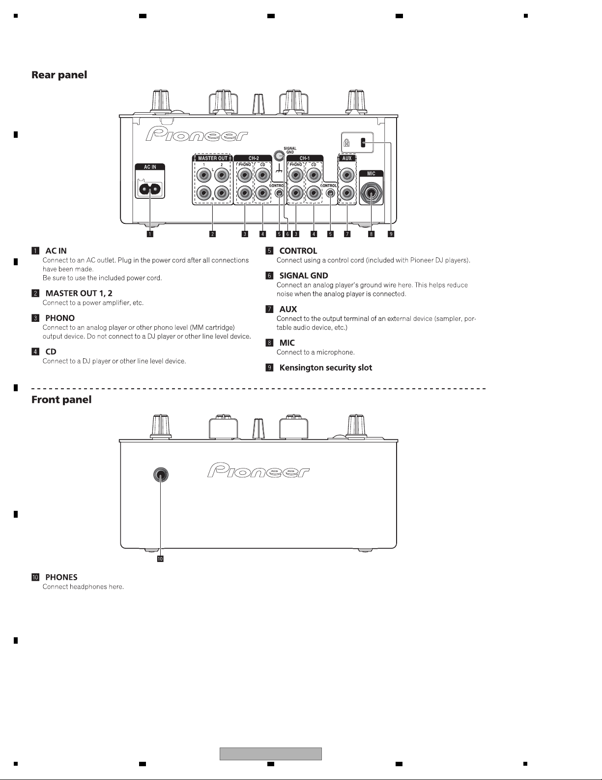
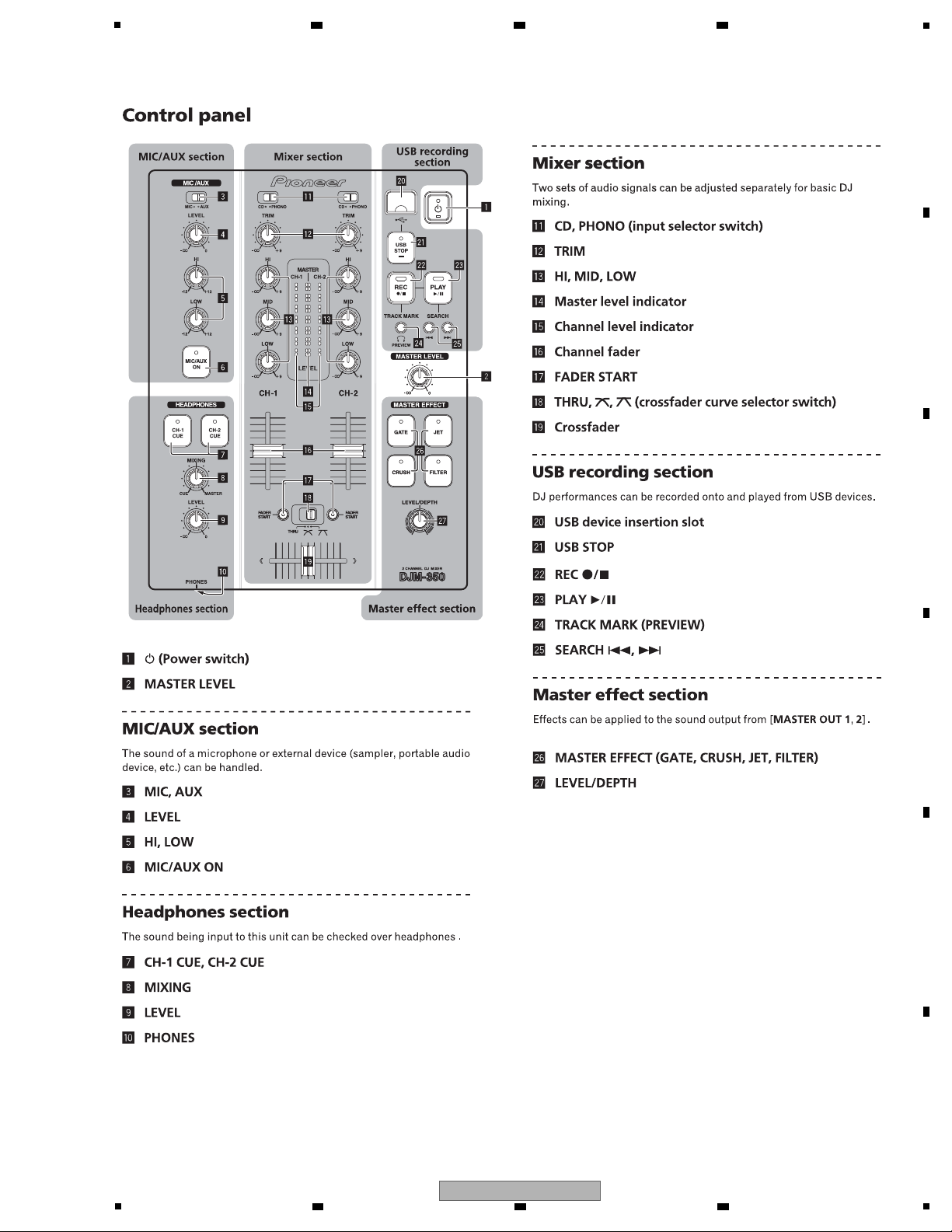
2.2 PANEL FACILITIES
A
B
2 3 4
C
D
E
F
8
1
2 3 4
DJM-350
5
6 7 8
A
B
C
D
E
F
DJM-350
5
6 7 8
9
1
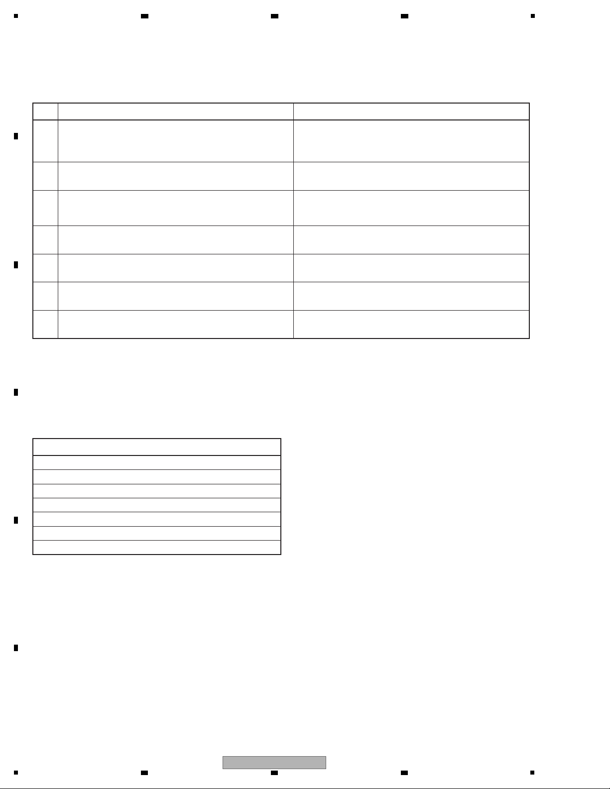
Item to be checked regarding audio
Distortion
Noise
Volume too low
Volume too high
Volume fluctuating
Sound interrupted
No. Procedures Check points
1
2
3
4
5
6
7
Playback data contained in the device connected to USB A Audio and operations must be normal.
Confirm whether the customer complain has been solved.
If the customer complain occurs with the specific source, such
as Mic, each Input, Fader, Equalizer, and Trim, input that
specific source for checking.
The customer complain must not be reappeared.
Audio and operations must be normal.
Check the analog audio playback.
(Make the analog connections with a CDJ player.)
Audio for each channel and operations must be normal.
Check playback by Fader operation.
(Select Fader and check the multichannel operations via the
CPU.)
Audio for each channel and operations must be normal.
Check the master outputs.
(Connect with a CDJ player.)
Audio and operations must be normal.
Check the sound from headphone output. Sound must be normal, without noise.
Check the appearance of the product. No scratches or dirt on its appearance after receiving it for
service.
Items to be checked after servicing / DJM
To keep the product quality after servicing, confirm recommended check points shown below.
See the table below for the items to be checked regarding audio.
2 3 4
3. BASIC ITEMS FOR SERVICE
3.1 CHECK POINTS AFTER SERVICING
A
B
C
D
E
F
10
1
2 3 4
DJM-350
5
A
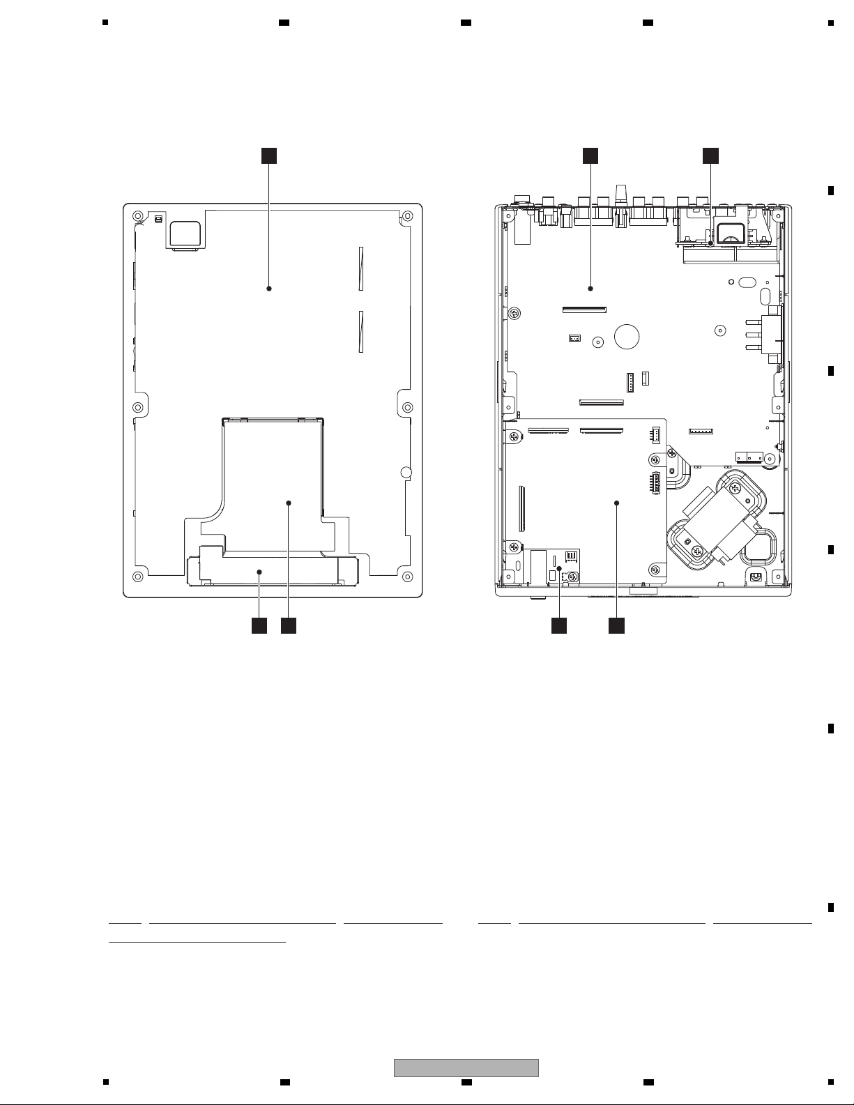
JACK ASSY
C
VRSW ASSY
• Bottom view
F
USJK ASSY
G
MAIN ASSY
E
FADR ASSY
B
HPJK ASSY
D
CRFD ASSY
1..MAIN ASSY DWX3112
1..JACK ASSY (SYXJ8, KXJ5, AXJ5) DWX3136
1..JACK ASSY (CUXJ) DWX3135
1..JACK ASSY (LXJ) DWX3116
NSP 1..PANL ASSY DWM2383
2..HPJK ASSY DWX3114
2..USJK ASSY DWX3115
2..VRSW ASSY DWX3117
2..FADR ASSY DWX3118
2..CRFD ASSY DWX3119
Mark No. Description Part No. Mark No. Description Part No.
LIST OF ASSEMBLIES
NOTES: - Parts marked by “NSP” are generally unavailable because they are not in our Master Spare Parts List.
-
The > mark found on some component parts indicates the importance of the safety factor of the part.
Therefore, when replacing, be sure to use parts of identical designation.
3.2 PCB LOCATIONS
6 7 8
A
B
C
5
6 7 8
DJM-350
D
E
F
11
1
D
CRFD ASSY
(DWX3119)
E
FADR ASSY
(DWX3118)
F
U
(D
VRSW ASSY
(DWX3117)
C
C C
1/3- 3/3
JA
(S
(C
(L
A
MAIN ASSY
(DWX3112)
G
G G
1/3- 3/3
MIC AUX CONT_1
CH1
CD/P
CN 1003
AKM1275-A
1
GN DD
2
USB_DP
3
USB_DM
4
V+5USB
JA3
DKB
456
JA3005
DKB1103-A
3
R
2
1
L
JA3004
DKN1614-A
231
JA3006
VKB1243-A
231
VKN 1431-A
CN 1001
1
CH1_L
2
GN DA
3
GN DA
4
GN DA
5
CH1_R
6
GN DA
7
GN DA
8
GN DA
9
CH2_L
10
GN DA
11
GN DA
12
GN DA
13
CH2_R
14
GN DA
15
GN DA
16
MIC_L
17
GN DA
18
GN DA
19
GN DA
20
MIC_R
21
GN DA
22
MIC_SEL
23
GN DA
24
CH1_SEL
25
GN DA
26
CH2_SEL
27
V+3R3D
VKN 1435-A
CN 1004
1
V+3R3REF
2
GN D_REF
3
CH1_FADER
4
AD_AN1
5
CH2_FADER
6
AD_AN0
7
CRS_FADER
8
HP_LEV
9
POWER_ON_LED
10
HP_CUE
11
STBY_SW
12
KEY2
13
STBY_ON_LED
14
KEY1
15
AD_CE1
16
KEY0
17
AD_CE0
18
GR4
19
SCAN6
20
GR3
21
SCAN5
22
GR2
23
SCAN4
24
GR1
25
SCAN3
26
GR0
27
SCAN2
28
V+5LED
29
SCAN1
30
GN DD
31
SCAN0
VKN 1260-A
CN 5001
1
GN DA_POWER
2
V+12V
3
GN DA_POWER
4
GN DA_POWER
5
V-12V
6
GN DA_POWER
7
GN DA_POWER
8
GN DA_M
9
GN DA_M
10
MIC_R
11
GN DA_M
12
GN DA_M
13
GN DA_M
14
MIC_L
15
GN DA
16
GN DA
17
CH2_L
18
GN DA_2
19
GN DA_2
20
GN DA_2
21
CH2_R
22
GN DA
23
GN DA
24
GN DA
25
CH1_L
26
GN DA_1
27
GN DA_1
28
GN DA_1
29
CH1_R
VKN 1258-A
CN 5002
1
V+3R3D
2
CH2_SEL
3
GN DA
4
CH1_SEL
5
GN DA
6
MIC_SEL
7
GN DA(MIC)
8
MIC_R
9
GN DA(MIC)
10
GN DA(MIC)
11
GN DA(MIC)
12
MIC_L
13
GN DA(MIC)
14
GN DA(CH2)
15
CH2_R
16
GN DA(CH2)
17
GN DA(CH2)
18
GN DA(CH2)
19
CH2_L
20
GN DA(CH2)
21
GN DA(CH1)
22
GN DA(CH1)
23
CH1_R
24
GN DA(CH1)
25
GN DA(CH1)
26
GN DA(CH1)
27
CH1_L
VKN 1291-A
CN 5004
1
SCAN0
2
GN D_D
3
SCAN1
4
V+5LED
5
SCAN2
6
GR0
7
SCAN3
8
GR1
9
SCAN4
10
GR2
11
SCAN5
12
GR3
13
SCAN6
14
GR4
15
AD_CE0
16
KEY0
17
AD_CE1
18
KEY1
19
STBY_LED
20
KEY2
21
STBY_SW
22
HP_CUE
23
PON_LED
24
HP_LEV
25
CRS_FADER
26
AD_AN0
27
CH2_FADER
28
AD_AN1
29
CH1_FADER
30
GN D_REF
31
V+3R3REF
VKN 1241-A
CN 6001
1
CH2_FADER
2
CH1_FADER
3
CRS_FADER
4
V+3R3REF
5
GN D_REF
6
KEY27KEY1
8
S09S1
10
G4
CN 6002
52147-0310
1
V+3R3REF2CRS_FADER3GN D_REF
51048-0300
JH7001
1
V+3R3REF
2
CRS_FADER
3
GN D_REF
VKN 1241-A
CN 5003
1
CH2_FADER
2
CH1_FADER
3
CRS_FADER
4
V+3R3REF
5
GN D_REF
6
KEY27KEY1
8S09
S110G4
VKN 1260-A
CN 3005
1
CH1_R
2
GN DA
3
GN DA
4
GN DA
5
CH1_L
6
GN DA
7
GN DA
8
GN DA
9
CH2_R
10
GN DA
11
GN DA
12
GN DA
13
CH2_L
14
GN DA
15
GN DA
16
MIC_L
17
GN DA
18
GN DA
19
GN DA
20
MIC_R
21
GN DA
22
GN DA
23
GN DA
24
GN DA
25
V-12V
26
GN DA
27
GN DA
28
V+12V
29
GN DA
CN 4501
KM200NA4L
1
GN DD
2
USB_DP
3
USB_DM
4
V+5USB
DDD1529-
FFC 31PIN
P=1.0 L=155mm
REVERSE
D20PDY0305E
JUMPER 3PIN
P=2.0 L=50mm
DDD1530-
FFC 27PIN
P=1.0 L=245mm
REVERSE
DDD1531-
FFC 29PIN
P=1.0 L=240mm
REVERSE
DKP38674PIN PH-PH
P=2.0 L=190mm
DDD1533FFC 10PIN
P=1.0 L=55mm
STRAIGHT
2 3 4
4. BLOCK DIAGRAM
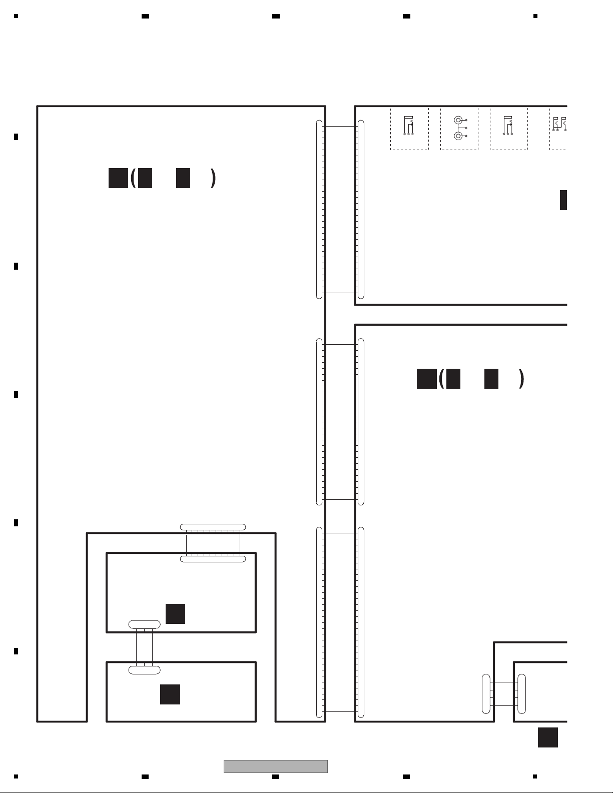
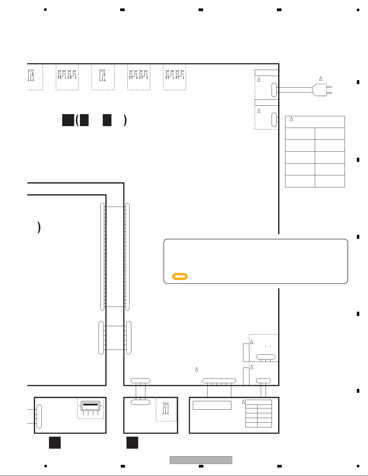
4.1 OVERALL WIRING DIAGRAM
A
B
C
D
E
F
12
1
2 3 4
DJM-350
5
F
USJK ASSY
(DWX3115)
B
HPJK ASSY
(DWX3114)
JACK ASSY
(SYXJ8,KXJ5,AXJ5: DWX3136)
(CUXJ: DWX3135)
(LXJ: DWX3116)
A
A A
1/5- 5/5
3/3
CH1
CD/PHONOCONT_2
CH2
CD/PHONO MASTER1/2_OUT
MAIN TRAN S
AXJ5 DTT1253LXJ DTT1250-
DTT1253-
DTT1253-
SYXJ8
CUXJ DTT1252KXJ5
!
!
!
!
!
!
!
!
JA3003
DKB1083-A
12345
6
JA3002
DKB1083-A
12345
6
CN 3006
KM200NA3
1
HP_L
2
GN DHP
3
HP_R
JA3008
DKB1083-A
12345
6
A3006
KB1243-A
231
JA3007
VKB1243-A
231
VKN 1433-A
CN1002
1
CH1_SEL_OUT
2
CONT2-2
3
CONT1-1
4
CONT2-1
5
CONT1-2
6
CH2_SEL_OUT
7
MIC_SEL_OUT
8
GN D_HP
9
GN D_HP
10
GN D_HP
11
HP_L
12
GN D_HP
13
GN D_HP
14
GN D_HP
15
HP_R
16
GN D_MAS
17
GN D_MAS
18
MAS_L
19
GN D_MAS
20
GN D_MAS
21
GN D_MAS
22
MAS_R
23
GN D_MAS
24
GN D_MAS
25
POWER_DOWN
26
XPROTECT
27
CPU_MUTE
28
GN DD
29
RELAY
VKN 1260-A
CN3007
1
CH1_SEL
2
CONT2-2
3
CONT1-1
4
CONT2-1
5
CONT1-2
6
CH2_SEL
7
MIC_SEL
8
GN DA
9
GN DA
10
GN DA
11
HP_L
12
GN DA
13
GN DA
14
GN DA
15
HP_R
16
GN DA
17
GN DA
18
MAS_L
19
GN DA
20
GN DA
21
GN DA
22
MAS_R
23
GN DA
24
GN DA
25
POWER_DOWN
26
XPROTECT
27
CPU_MUTE
28
GN DD
29
RELAY_CTRL
JA3001
DKP3860-A
1
LIVE
2
NEUTRAL
B6B-EH
CN 3003
1
2
345
6
CN 4001
KM200NA3L
1
HP_L
2
GN DHP
3
HP_R
CN 4501
KM200NA4L
1
GN DD
2
USB_DP
3
USB_DM
4
V+5USB
JA4001
DKN1622-A
2
3
1
DKB1106-A
JA4502
123
4
RT1
RT2
JA3001
DKP3861-A
1
LIVE
2
NEUTRAL
B2P3-VH
CN 3002
1
NEUTRAL2LIVE
B3P5-VH
CN 3001
1
NEUTRAL
2
110
120V
3
220
240V
KM200NA6
CN3004
1
V+5A
2
GN DA
3
V+5D_UN REG
4
V+5D_UN REG
5
GN DD
6
GN DD
AKM1277-A
CN1005
1
V+5A
2
GN DA
3
V+5D_UN REG
4
V+5D_UN REG
5
GN DD
6
GN DD
L=190mm
DDD1532-
FFC 29PIN
P=1.0 L=95mm
STRAIGHT
DKP38683PIN PH-PH
P=2.0 L=200mm
VH 2PIN
L=160mm
EH 6PIN
L=145mm
MAIN TRAN S
AC CORD
SYXJ8
CUXJ
KXJ5
AXJ5
LXJ
ADG7022-
ADG7079-
ADG1154-
ADG1154-
XDG3054-
AC INLET
(CUXJ only)
AC1
AC2
GN DA
AC3
AC4
AC5
LXJ only
PF06PP-S12
6PIN PH-PH
P=2.0 L=130
AC INLET
(others)
others
-
When ordering service parts, be sure to refer to "EXPLODED VIEWS
and PARTS LIST" or "PCB PARTS LIST".
-
The > mark found on some component parts indicates the importance
of the safety factor of the part.
Therefore, when replacing, be sure to use parts of identical designation.
-
: The power supply is shown with the marked box.
6 7 8
A
B
C
D
E
F
5
6 7 8
DJM-350
13
1
INPUT SW select
CH1
CH2
MIC/AUX
RIAA RIAA
RIAA RIAA
40dB
-
+
-
+
-
+
IC1025
AK5358AET
ADC(CH-1)
IC1027
AK5358AET
ADC(CH-2)
IC1026
AK5358AET
ADC(MIC)
-
+
Hi
Lo
CN3007(2/2) CN1002(2/2)
IC5003(2/2)
NJM4565MD
7
6
7
5
IC5004(2/2)
NJM4565MD
7
5
7
5
IC5002(2/2)
NJM4565MD
IC5001(2/2)
NJM4565MD
9
19
16
12
1
27
226
262
24
4
CN5002 CN1001
16
1313
55
16
CN5002
CN1001
MIC TRIM
CH2 TRIM
CH1 TRIM
MIC
AUX
PHONO
CD
PHONO
CD
CH 1
CH 2
JA3002
JA3003
JA3004
JA3005
3
8
ch A
ch B
1
2
5
7
6
4
3
8
ch A
ch B
1
2
5
7
6
4
3
8
ch A
ch B
1
2
5
7
6
4
JACK ASSY (1/2)
A
VRSW ASSY (1/2)
C
2
2
2
9
9
9
77
66
11
2 3 4
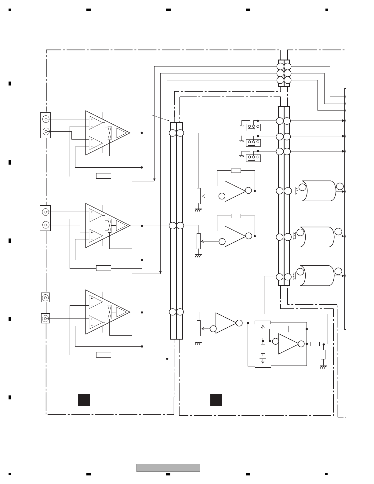
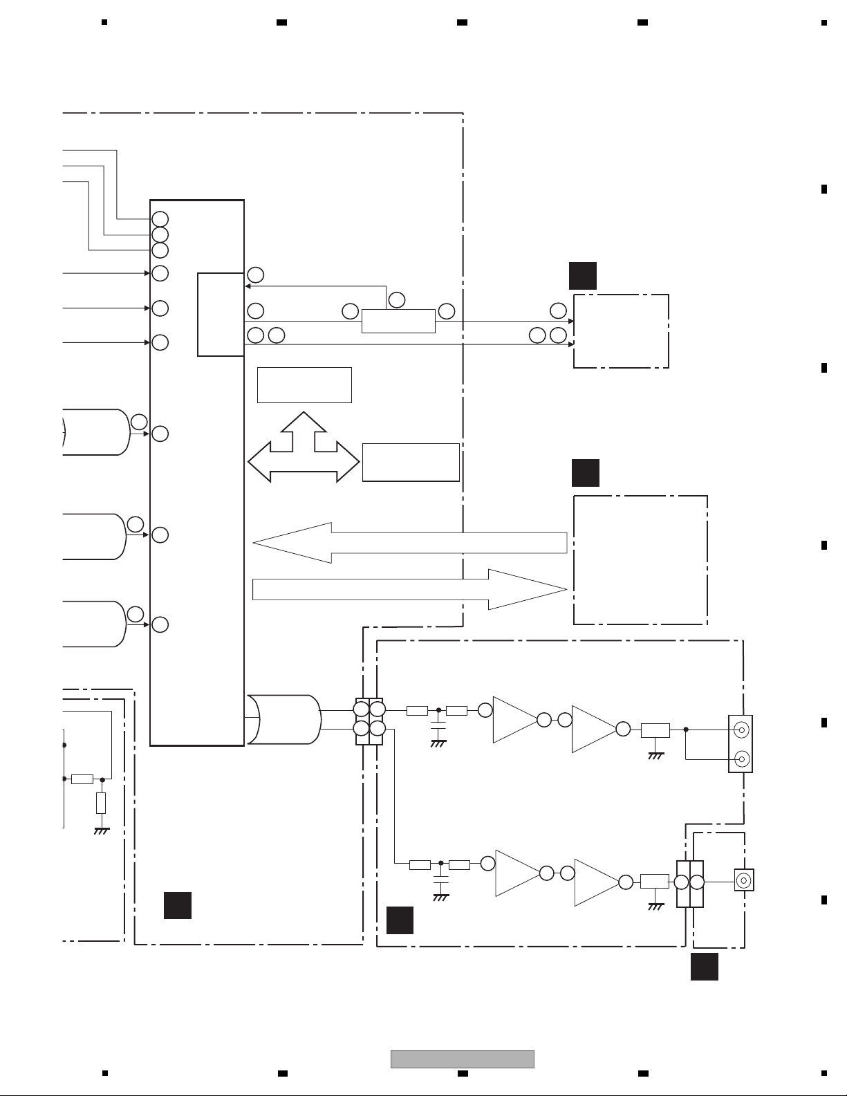
4.2 OVERALL BLOCK DIAGRAM
A
B
C
D
E
F
14
1
2 3 4
DJM-350
5
Over-current Detecion
,
IC1002
CPU
R5S72630P200FP
KEY, SW, FADER etc
DM, DP
VBUS
LEVEL METER etc
VR, SW
IC1011
DYW1794
FLASH 8Mbit
LED
BUS
IC1019
R5523N001B
USB
Function
Mute
Mute
Mute
PHONES
MASTER
OUT
IC1025
AK5358AET
ADC(CH-1)
IC1027
AK5358AET
ADC(CH-2)
IC1026
AK5358AET
ADC(MIC)
IC1030
AK4359AEF
Multi-DAC
IC3013(1/2)
RNB4580F
IC1010
K4S641632N-LC75
SDRAM 64M
7
7
6
-
+
6
-
+
IC3012(2/2)
NJM4565MD
IC3011(1/2)
NJM4556AD
7
1 6
-
+
-
+
IC3010(1/2)
NJM4565MD
2
CN3007(1/2)
18
18
11
11
1
1
CN1002(1/2)
MAIN ASSY
G
JACK ASSY (2/2)
A
HPJK ASSY
B
VRSW ASSY (2/2)
C
USJK ASSY
F
9
9
9
145
86
69
102
101 100
,
3 2
4
4 5
3
83
85
150
149
158
139
134
6 7 8
A
B
C
D
5
6 7 8
DJM-350
E
F
15
1
IC1018
BD9326EFJ
V+5USB
V+LED
2200uF
/25V
V+5D_UNREG
(7-16V)
V+3.3D
V+1.2D
IC1039
BH33FB1WG
SH7263
MUTE
Reset
Signal
IC1020
BD9106FVM
IC1038
NJM2392M
Relay Cont
Relay Cont
MAIN TRANS.
STANDBY TRANS.
T3001
V+5D_UNREG
V+5A
2200uF
/35V
IC3001
BA05T
100uF
/16V
IC3002
KIA7812API
1000uF
/35V
V+12A
+
+
+
++
+
V-12A
IC3003
KIA7912PI
1000uF
/35V
100uF
/16V
100uF
/16V
P3002
2200uF
/25V
+
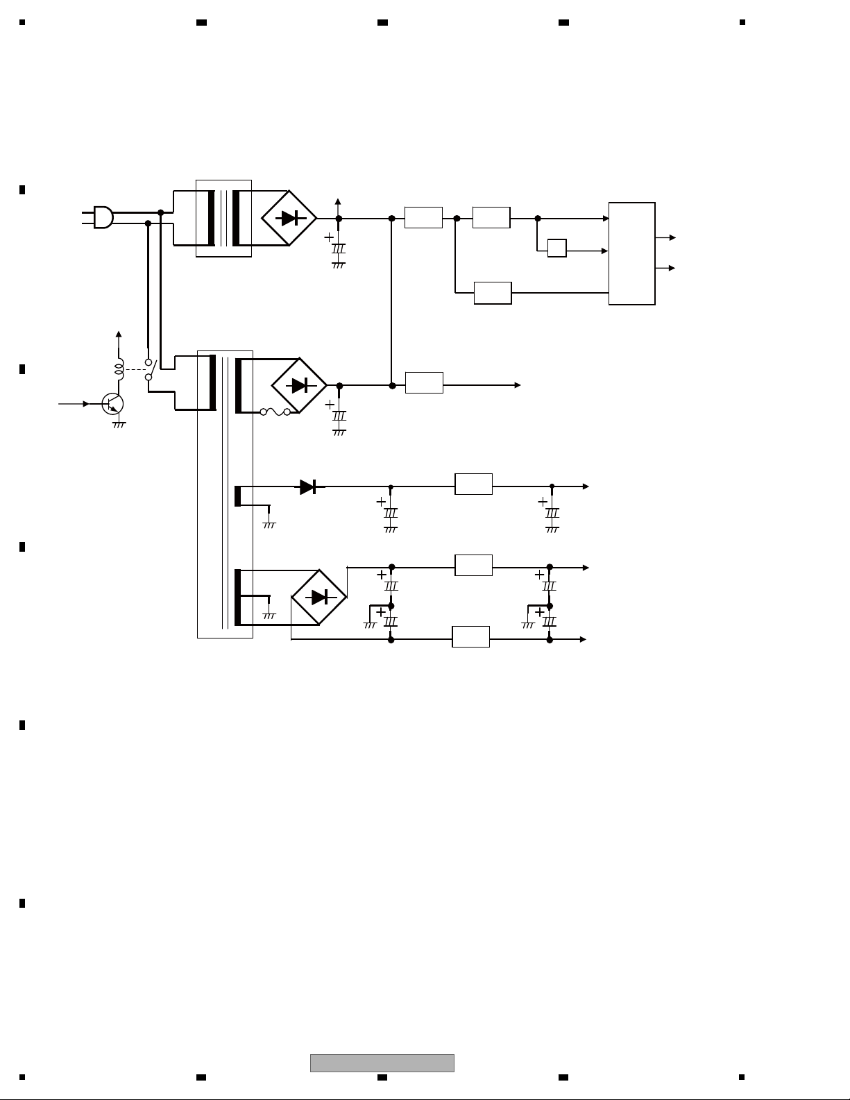
4.3 POWER BLOCK DIAGRAM
A
B
2 3 4
C
D
E
F
16
1
2 3 4
DJM-350
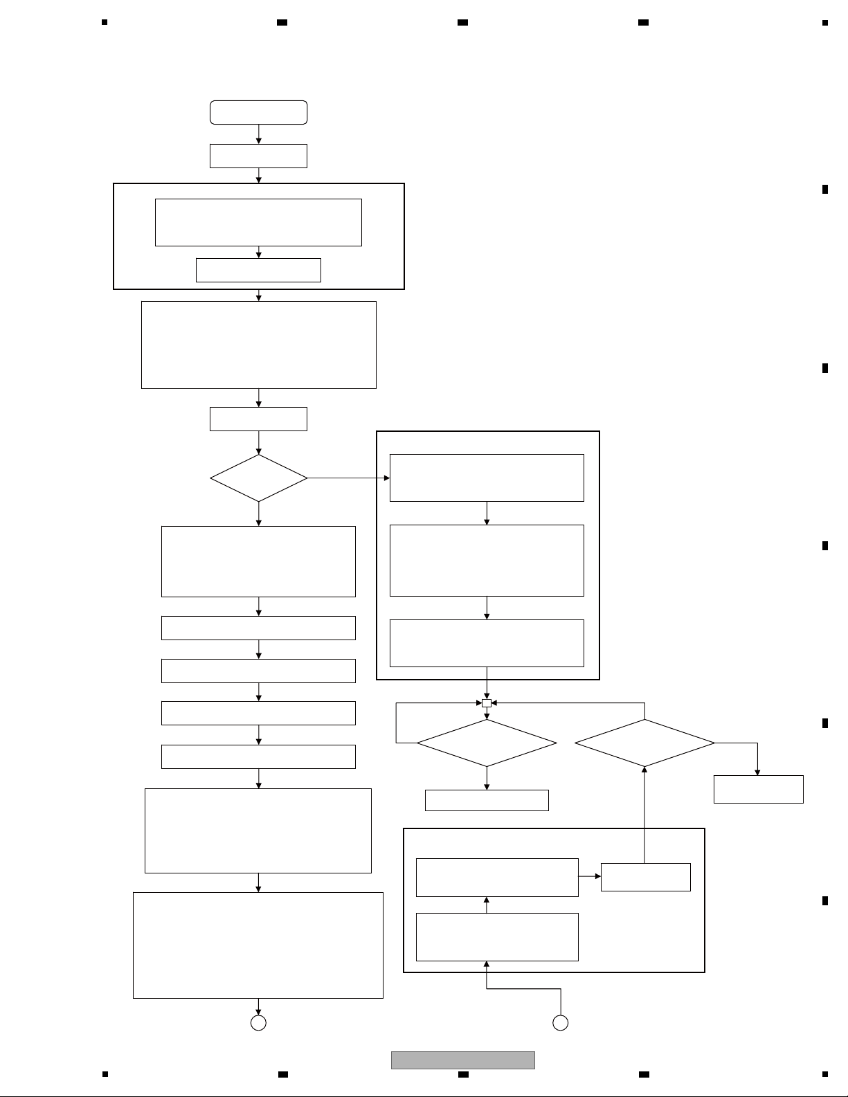
5
Setting for shifting to Standby at startup
Eco mode at startup
AC OFF to AC IN
[Set the CPU operation clock to the minimum value.]
Internal: 133 MHz, Bus: 66 MHz, Periphery: 33 MHz
↓
Internal: 133 MHz, Bus: 66 MHz, Periphery: 11 MHz
Reading Standby
flag register
Is Standby
canceled?
[Port setting for Standby mode]
MIC/CH1/CH2 input selector port: Low output
Is the Standby
button released?
Standby mode
NO
YES
NO
YES
[SDRAM self-refreshment]
[Essential GPIO settings]
CPU_MUTE port setting : MUTE ON
Main transformer relay port setting: Relay OFF
V+5LED port setting : OFF
Power LED port setting : Red LED: Lit, Green LED: Unlit
Standby button port setting : Input port
AD/DA converter port setting : Reset state
Port setting for M clock : OFF
[Standby setting]
• Standby register setting
• FLASH: Low power-consumption setting
• SDRAM self-refreshment setting
[Preprocessing of relay ON]
• Green Power LED: Lights.
• Preceding canceling of CMT module standby
• Muting ON
• DA/AD powerdown
• Stop of M clock
[Relay ON]
Waiting for 300 msec for power stabilization
[V+5LED ON]
Waiting for 300 msec for stabilization of V+5LED
[Port setting 2 for Standby mode]
SSI data output port: Fixed at low
LED scan port: Low output
AD multiplexer selection port: Low output
Green power LED port: Input enabling HiZ
Is an abnormal voltage
a cause of error?
Detection of
abnormal voltage
YES
NO
START
Final setting for shifting to Standby mode
during operation
[HW setup for normal operation]
CPG setting : Internal: 200 MHz, Bus: 66 MHz,
Periphery: 33 MHz
PFC setting : Settings of all ports (V+5USB: ON)
BSC setting : For SDRAM
INTC setting : Setting for disabling interruption,
Register bank ALL setting
SCIF setting : Serial setting for DAC
[Determination of Startup mode]
Reading of all corresponding keys
No key pressed: Normal mode
[CH1 FADER START] + [CH2 FADER START]: Update mode
[SEARCH FWD] + [SEARCH BACK]: EUP Setup mode
[CH1 CUE] + [CH1 FADER START] + [GATE]: TEST1
[CH1 CUE] + [CH1 FADER START] + [JET] = TEST2
[CRUSH] + [FILTER]: Version indication
[GATE] + [JET]: All LEDs lit
[Standby setting]
• Standby resistor setting
• FLASH: Low power-consumption setting
• SDRAM self-refreshment setting
[Main transformer relay OFF]
V+5LED is set to OFF to set the main
transformer relay to OFF.
Waiting for 1.6 sec
A B
5. DIAGNOSIS
5.1 POWER ON SEQUENCE
6 7 8
A
B
5
6 7 8
DJM-350
C
D
E
F
17
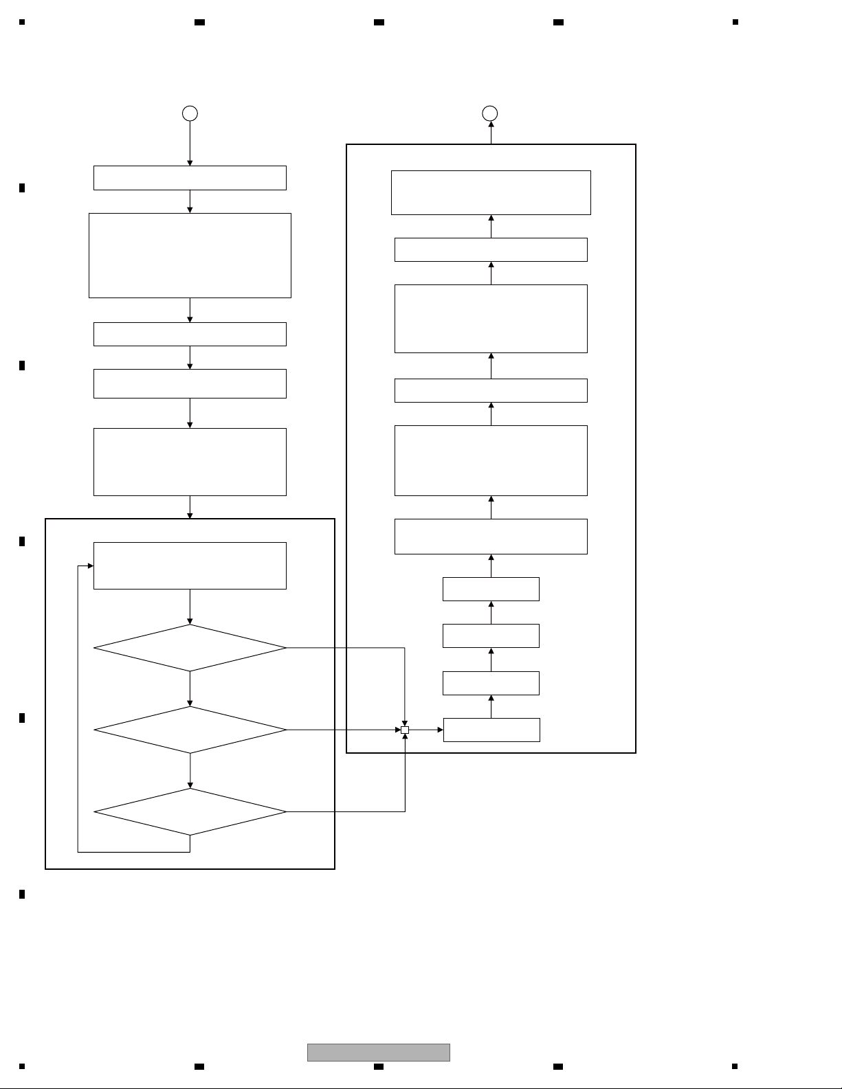
1
Setting for shifting to Standby mode during operation
Power ON
[Normal mode]
Process corresponding to each mode
Is shifting to Standby mode
commanded by Standby button?
YES
NO
YES
V+5USB to OFF, corresponding to Startup mode.
[RAM initialization and loading of essential programs]
• All regions of SDRAM: Null
• Null everything other than internal RAM stack.
• Transferring a temporary vector table and entity to
internal RAM.
• Transferring a slow-operation program for Eco
mode to retention RAM.
• Transferring IPL from FLASH-ROM to SDRAM.
Setting vector base register to internal RAM
[Cache setting]
Enables only instruction cache
[Jumping to program loader]
• If an error in firmware updating is detected,
the program for emergency booting will be
transferred to the SDRAM.
• In cases other than the above, the program for
normal startup will be transferred to the SDRAM.
V+5USB: OFF
PWM output: OFF
AD conversion: Stop
[Port setting for Standby mode]
MIC/CH1/CH2 input selector port: Low output
SRC : Stop
SSI output : Muting
ADC power : OFF
SSI input : Muting
DAC power : OFF
Stop of M clock
DMA: Stop
All modules other than CMT: Standby
Is the AC-OFF flag ON?
Is the Power failure flag ON?
NO
YES
NO
Muting ON
A B
[Set the CPU operation clock to the minimum value.]
Internal: 133 MHz, Bus: 66 MHz, Periphery: 33 MHz
↓
Internal: 133 MHz, Bus: 66 MHz, Periphery: 11 MHz
[Port setting 2 for Standby mode]
SSI data output port: Fixed at low
LED scan port: Low output
AD multiplexer selection port: Low output
Green power LED port: Input enabling HiZ
* Eco mode:
Low-speed and low-power-consumption mode provided for the CPU
to be operated only on power supply from the standby transformer.
2 3 4
A
B
C
D
E
F
18
1
2 3 4
DJM-350
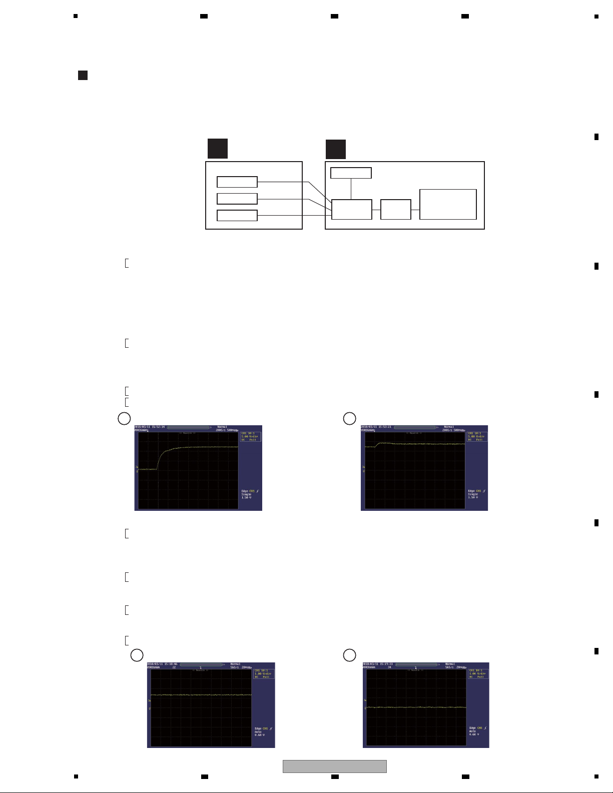
5
11
2 2
(MAIN)
(JACK) (JACK)
(MAIN)
Symptom: The STBY LED flashes and no key is operable.
Status of the product:
The CPU, detecting that a power failure had been generated, shut the main transformer off, instructed the STBY LED to flash,
and disabled the keys. (When the main transformer is shut off, the relay (RY3001) is set to OFF and power is not supplied
to the main transformer.)
Troubleshooting of the Power System
Circuit block diagram
Diagnostic procedure
For diagnosis, plug in then unplug the AC power cord for each measurement, and perform measurement of
each point within about 10 sec.
1 While the STBY LED is flashing, check that the output from the TEST pin (Detect FLAG) near R1190 is
low (abnormal). *If it is high, nothing is wrong with the voltage.
2 Remove R1190 and plug the AC power cord in.
*Unplug the AC power cord after about 10 sec, because power will be forcibly supplied to the main transformer
even if any voltage is abnormal. (If abnormal voltage continues, the defective point may produce heat, which
may be dangerous.)
3 Check the voltages at the diagnostic points described below.
The circuit or power IC that is connected to the part whose voltage is abnormal may be defective.
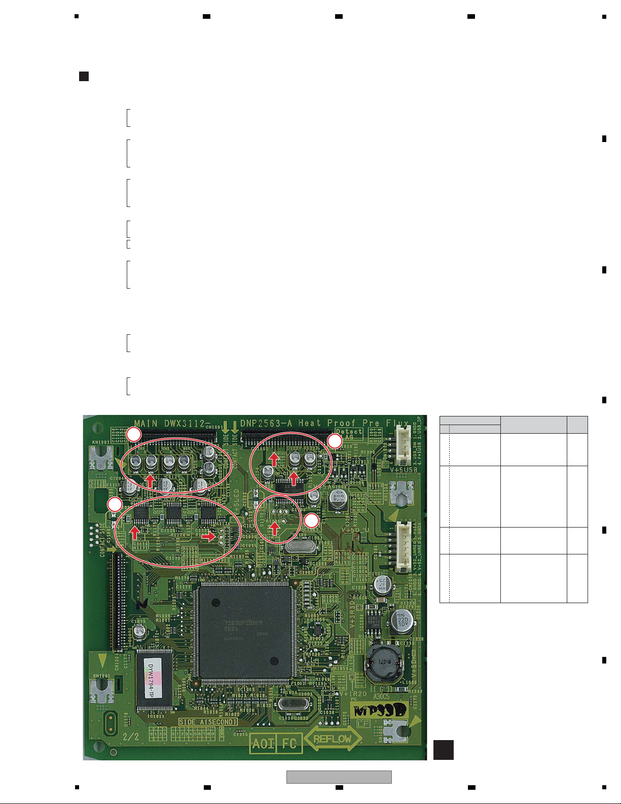
JACK Assy: Voltages can be checked at the J3023, J3054, and J3038 jumpers.
Note: After diagnosis is completed, be sure to place R1190 to its original position.
Symptom: The STBY LED does not light and the product does not operate at all, even after the AC
power cord is plugged in.
1 Check the voltage of V+5D_U power.
⇒ If the voltage does not become high, check conduction at the protector (P3002).
Symptoms caused by other power failure
Symptom: Malfunction of a USB device
2 If the protector is intact, check each voltage on the MAIN Assy.
• V+5D ⇒ +5 V, • V+3R3D ⇒ +3.3 V, • V+1R2D ⇒ +1.2 V,
Check that the voltage of V+5USB power is +5 V.
IC3002
V+12A
V-12A
V+5A
V+5LED
IC1018
IC3003
IC3001
Detection
Circuit
CPU (IC1002)
pin 66
Detect FLAG
R1190
(0 Ω)
Change in V+5D_U when the AC power cord is plugged in Change in V+5D_U when the power switch is set to ON
While power is ON (relay: ON) Section H (J3067) During STBY (relay: OFF) Section H (J3067)
A
JACK ASSY
G
MAIN ASSY
Section A
Section B
Section C
Section D
Section E
Section F
Symptom: Defective operations of various VRs, such as equalizers, etc.
Check that the positive voltage of the capacitor at Section F is +3.3 V.
Section F
Symptom: Power is not supplied to the main transformer.
Check that the proper control signal is input to the relay circuit (J3067).
Section H
6 7 8
5.2 TROUBLESHOOTING
A
B
C
D
5
6 7 8
DJM-350
E
F
19
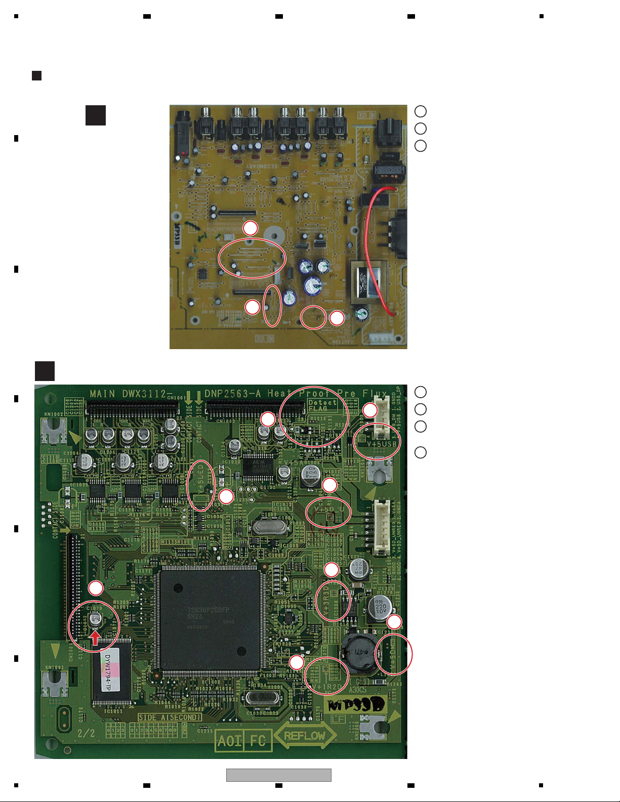
1
A
JACK ASSY
G
MAIN ASSY
B
B
H
D
A
F
C
F
E
E
E
F
: J3023, J3054, J3038
D
: P3002
H
: J3067
A
: Test p / Detect FLAG
C
: Test p / V+5D_U
E
: Test p / V+5D, V+3R3D,
V+1R2D
F
: Test p / V+5USB, V+5LED,
C1079 (+) pin
Measuring Points of the Power System
A
2 3 4
B
C
D
E
F
20
1
2 3 4
DJM-350
5
Symptom: Audio is not output.
Diagnostic points:
Symptom: The CD and PHONO inputs cannot be switched.
• Is a signal input to the ADC (IC1025: ch1, IC1026: mic, IC1027: ch2 → Pins 1 and 2)?
⇒ If it is not, something is wrong with the analog-circuit block.
• Are analog signals input to the VRSW Assy?
⇒ If they are not, something is wrong with the input-circuit section on the JACK Assy.
If they are, something is wrong with the analog block on the VRSW Assy.
• Is a digital signal output from the ADC (IC1025: ch1, IC1026: mic, IC1027: ch2 → Pin 9)?
Is a CLK signal input to the ADC (IC1025: ch1, IC1026: mic, IC1027: ch2 → Pins a, b, and c)?
⇒ If there is no output from Pin 9 although the CLK signal is input, the ADC may be in failure.
• Is a signal output from analog output of the DAC (IC1030 → Pins l and m: MASTER, Pins o and p: HP)?
⇒ If it is, something is wrong with the JACK Assy.
The MUTE circuit (J3015) may be in failure.
• Is a signal input to the digital input of the DAC (IC1030 → Pin 3)?
Is a CLK signal input to the DAC (IC1030 → Pins 1, 2, and 4)?
⇒ If no signal is output even if a digital signal is input properly, the DAC may be in failure.
The VRs may be in failure.
Check operations of each VR in Service mode.
• Is a normal switching signal input to each input operational amp (J3028: ch1, J3058: ch2)?
⇒ If it is, an input operational amp may be in failure.
Symptom: The MIC and AUX inputs cannot be switched.
• Is a normal switching signal input to each input operational amp (J3093: mic)?
⇒ If it is, an input operational amp may be in failure.
Troubleshooting of the Analog Signal System
Section A
G
MAIN ASSY
A
C
D
F
Diagnosis Point
Point
Measurement Point
CN1001
1, 5 pin
9, d pin
g, k pin
A/DC input
CH1_L, R
CH2_L, R
MIC_L, R
IC1025 9 pin
IC1027 9 pin
IC1026 9 pin
R1157
R1109
R1108
A/DC Digital output
CH1
CH2
MIC
A/DC CLK
AUDIO_CLK2
AD_3R072M
AD_48k
IC1030 3 pin
IC1030 1 pin
IC1030 2 pin
IC1030 4 pin
D/AC Digital input
MASTER/HP_DATA
D/AC CLK
AUDIO_CLK3
DA_6R144M
DA_48k
A
C
4
CN1002
i, m pin
b, f pin
D/AC Analog output
MASTER_L, R
HP_L, R
D
F
6
e
f
g
h
7
a
b
c
d
Measurement Signal
Waveform
No.
Section B
Section C
Section F
Section G
Section G
Section D
Section E
6 7 8
A
B
C
D
E
F
DJM-350
5
6 7 8
21
1
A
JACK ASSY
C
VRSW ASSY
B
I
H
E
G G G
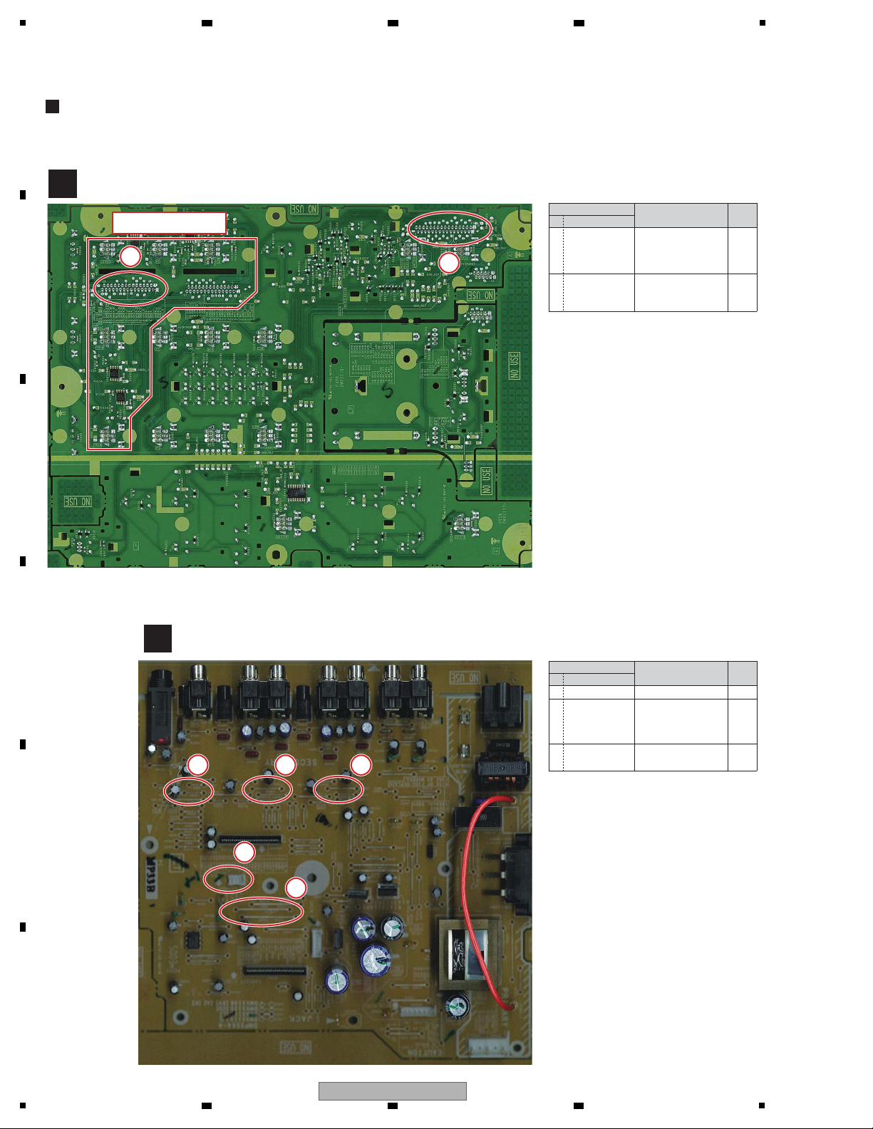
Analog Block
Diagnosis Point
Point
Measurement Point
CN5001
1, 5 pin
9, d pin
g, k pin
VRSW Assy Analog input
CH1_R, L
CH2_R, L
MIC_L, R
CN5004
1 pin
6 pin
LED lit, Key read related signal
SCAN0
GR0
B
I
5
k
l
Measurement Signal
Waveform
No.
Diagnosis Point
Point
Measurement Point
J3015 MUTE
E
G
i
j
CN3006
1, 3 pin
Headphone output
HP_L, R
J3028
J3058
J3093
CD/PHONO switch
CH1_L
CH2_L
MIC/AUX switch
H
9
Measurement Signal
Waveform
No.
Measuring Points of the Analog Signal System
A
2 3 4
B
C
D
E
F
22
1
2 3 4
DJM-350
5
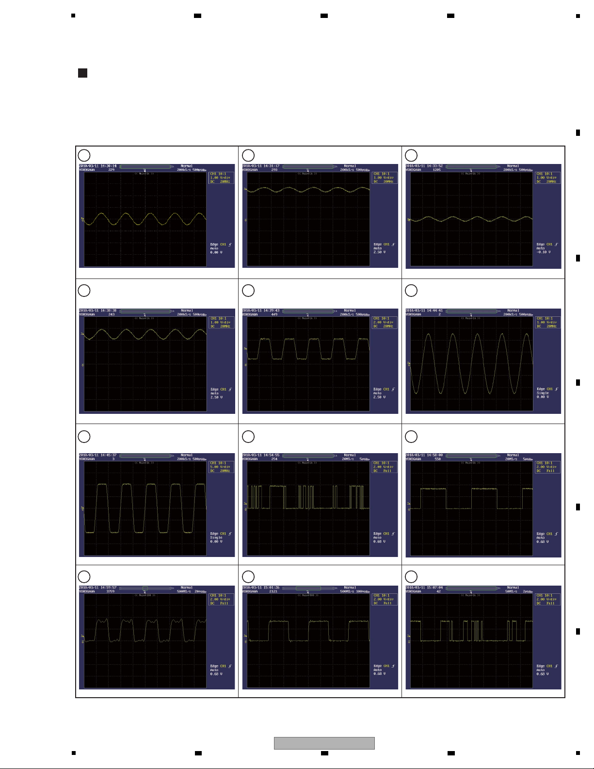
CD1L input (JACK) PIN JACK ADC input (MAIN) Section A PANEL input (VRSW) Section B
DAC output (MASTER) (MAIN)
Section D
DAC output (HP) (MAIN)
Section D
HP OUT (no termination) (JACK)
Section H
ADC 9 pin (MAIN)
Section C
ADC 10 pin (MAIN)
Section C
ADC 11 pin (MAIN) Section C ADC 12 pin (MAIN) Section C DAC 3 pin (MAIN) Section F
MASTER1L output (JACK)
PIN JACK
3 4 5
6 7 8
9 10 11
12 13 14
Setting of each control:
TRIM, MASTER LEVEL, HP LEVEL, and CH FADER: to MAX
Set other VRs to their center positions. Set the curve switch to THRU.
Set the input to CH1-CD L, 1.0 Vp-p/1 kHz. Set the output to OPEN.
Normal Waveforms at Each Section
6 7 8
A
B
C
D
E
DJM-350
5
6 7 8
F
23
1
15 16 17
18
19
18
20 21
19
DAC 1 pin (MAIN) DAC 2 pin (MAIN) Section F DAC 4 pin (MAIN) Section F
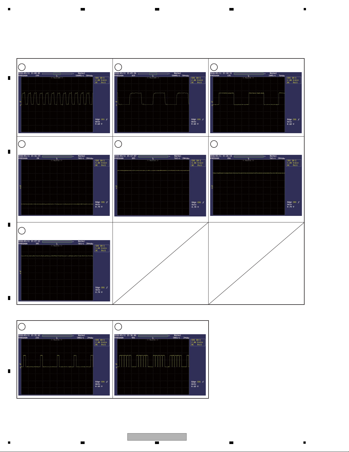
MUTE (power ON): MUTE is turned OFF.
(JACK)
Section E (J3015) Section E (J3015) Section G (J3028)
Section G (J3028)
Section F
MUTE (Standby): MUTE is turned ON.
(JACK)
PHONO is selected for CH1 input. (JACK)
(Reference) Signals related to lighting of the LEDs and reading of key data
SCAN0 (VRSW) Section I Section IGR0 (VRSW)
CD is selected for CH1 input. (JACK)
A
2 3 4
B
C
D
E
F
24
1
2 3 4
DJM-350

5
0
About errors
If this unit cannot operate normally, the [u] (the power switch), [USB STOP] and [PLAY f] indicators flash to indicate
an error.
Check the table below and take the measures indicated.
If the [USB STOP] indicator flashes repeatedly 2 to 5 times
1 Disconnect the USB device.
2 Press [USB STOP].
Check the table below and take the measures indicated.
About the [USB STOP] indicator’s error indication
Indicator
name
Number
of times
indicator
flashes
Description of
error
Cause Measure
USB STOP
2 times
repeatedly
File format problem
USB device is not formatted.
Use a USB device formatted with a file system sup
ported by this unit (FAT or HFS+).
-
You are using a USB device with a file system that is not
supported by this unit.
3 times
repeatedly
USB class problem
A device other than a USB mass storage class device is
connected.
Connect a USB mass storage class USB device.
A USB hub is connected. Do not connect USB hubs.
4 times
repeatedly
Problem writing
on the USB device
Not enough free space on the USB device. Use a USB device with sufficient free space.
There is a file name “REC999.WAV” in the recorded data
storage folder (PIONEER DJM / DJM350 REC).
Files created through recording are given a 3-digit number.
Once the number 999 is reached, no new files can be
created in the folder. If this happens, move the files in the
folder to a different folder.
USB device’s write protect switch is set to the on position. Set the USB device’s write-protect switch to the off
position.
You are using a USB device with a security function. Use a USB device without a security function.
The recorded data storage folder (PIONEER DJM /
DJM350 REC) is set to “Read Only”.
Change the setting so that the recorded data storage
folder is writable.
5 times
repeatedly
USB device over
current detected
-
You are using a USB device (such as a bus power-driven
hard disk) whose current is higher than this unit’s rated
current (500 mA).
Use a USB device within this unit’s rated current (such
as a hard disk driven by an AC adapter or other external
power supply).
PLAY f
3 times Playback error
There are no playable files in the recorded data storage
folder (PIONEER DJM / DJM350 REC).
Perform the recording operation on this unit to create
playable files before playing them.
u (power
switch)
Continuous Circuit problem There is a problem in the internal circuitry. Unplug this unit’s power cord from the power outlet.
6 7 8
5.3 ERROR INDICATION
A
B
C
D
E
F
DJM-350
5
6 7 8
25
1
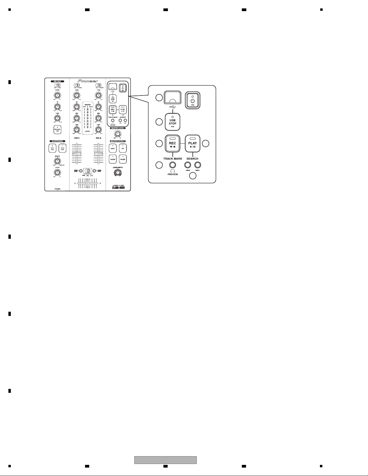
With this unit, DJ-played music (audio signals output from the MASTER OUT 1 and 2 connectors) can be recorded
into a USB device, such as a USB memory device, as a WAV file.
Follow the procedures below to check each operation.
For details, refer to "Recording musical performance," page 12 of the Operating instructions.
Immediately after a USB device is plugged into the USB device connector (1), the USB STOP indicator (2) starts flashing.
After a while, the USB STOP indicator stops flashing and stays lit, and the unit will be ready for recording.
To start recording, press the REC k/g key (3). The REC k/g indicator (3) will light.
To stop recording, press the REC k/g key again. The REC k/g indicator goes off.
To start playing back the recorded track, press the PLAY f key (4). The PLAY f indicator (4) will light.
To pause playback, press the PLAY f key again.
• Checking Fast Forward/Rewind operations
For Fast Forward or Rewind operation, hold the SEARCH o key or the SEARCH p key (6) pressed
during playback, respectively.
During Fast Forward/Rewind operation, the PLAY f indicator flashes.
• Preview check via the headphones
Turn and set the MIXING control to the leftward position from the center then hold the TRACK MARK (PREVIEW)
key (5) pressed. You can listen to the sound of the recorded tracks via the headphones while the key is being held.
From the headphones, sound of the WAV file mixed with CH-1 and CH-2 sound will be output.
1. Procedures for checking recording into a USB device
2. Procedures for checking playback of data in a USB device
2
1
3
5
6
4
5.4
OPERATION CHECK OF RECORDING / PLAYING / TO FROM A USB DEVICE
A
2 3 4
B
C
D
E
F
26
1
2 3 4
DJM-350
5
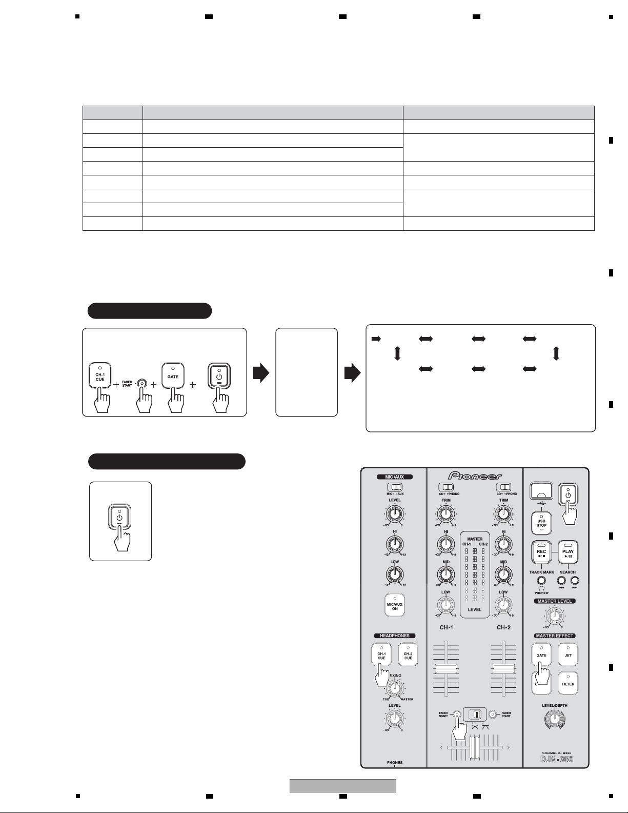
CH-1
FADER
START
button
GATE
button
CH-1
CUE
button
Mode 0
POWER ON
Mode 1 Mode 2
Mode 7 Mode 6 Mode 5
Mode 3
Mode 4
1. Description of Test Modes
2. Test Mode
Test Mode
(Mode 0)
Test Mode : ON
Test Mode : CANCEL
• Press the p key to shift to the next mode.
• Press the o key to shift to the previous mode.
• You can confirm the current mode number while you hold
the TRACK MARK (PREVIEW) key pressed (the level
meter indicates a numeric value).
POWER OFF
In Test mode, no audio processing is performed (no mixing function is available). To avoid any accidental failure,
never connect anything to the MASTER OUT connector or HEADPHONES output connector in Test mode.
Mode No. Description of The Modes Purpose of Use
0 Mode for version confirmation Confirmation of the version of the firmware
1 Mode for making all LEDs unlit
Confirmation of LED operations
2 Mode for making all LEDs lit
3 Mode for confirmation of individual keys Confirmation of operations of individual keys
4 Mode for confirmation of individual switches Confirmation of operations of individual switches
5 Mode for confirmation of the values of the rotary variable controls
Confirmation of operations of individual variable controls
6
Mode for confirmation of fluctuated values of the rotary variable controls
7 Mode for confirmation of the meter LEDs Confirmation of meter-LED operations
The Following eight test modes are provided for this unit:
6 7 8
6. SERVICE MODE
6.1 TEST MODE
A
B
C
D
E
F
DJM-350
5
6 7 8
27
1
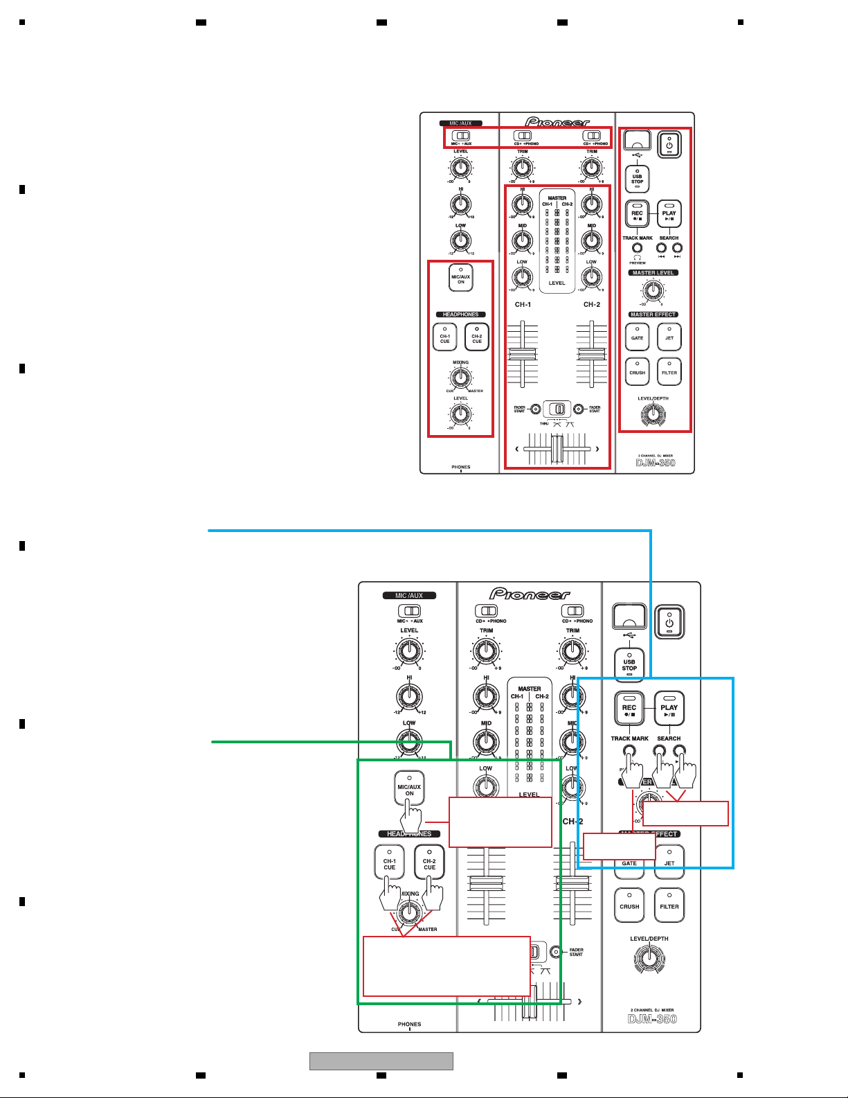
3. Test Possible Area
• The MIC LEVEL control is an exception to testing.
• The MIC equalizer (HI and LOW) controls are exceptions
to testing.
• The TRIM control is an exception to testing.
(The right controls are operating elements that are not
managed by the microcomputer.)
4. Basic Operation Method
Basic Operation Method
To switch Test modes, use the SEARCH key.
With this unit, the Test mode No. is not normally
indicated.
The Test mode No. is indicated on the level meter
while the TRACK MARK key is held pressed.
If the Test mode is advanced, the PLAY LED flashes
once.
If the Test mode is backtracked, the PLAY LED flashes
twice.
Basic Operation Method 2
(For details, see the descriptions for each mode):
In Test 6 mode, the individual operating elements can
be tested. In Test 6 mode, select an operating element,
using the CH-1 CUE or CH-2 CUE key.
If an unintended erroneous value is displayed when an
operating element is operated, you can reset it by
pressing the MIC/AUX ON key.
In Test 7 mode, the individual LEDs of the level meters
can be tested.
You can light the individual LEDs one after another,
using the CH-1 CUE, CH-2 CUE, or MIC/AUX ON key.
For indicating a
Test mode No.
[Mode 6]
Reset button
[Mode 7]
MASTER-LED button
[Mode 6]
For going forward/back one operating
element to be tested
[Mode 7]
CH1 and CH2-LED buttons
For going forward
/back one mode
A
2 3 4
B
C
D
E
F
28
1
2 3 4
DJM-350
 Loading...