

Page 1
CD RDS RECEIVER
ORDER NO.
CRT3904
DEH-P85BT/XN/EW5
DEH-P85BT
This service manual should be used together with the following manual(s):
Model No. Order No. Mech.Module Remarks
CX-3195 CRT3815 S10.5COMP2 CD Mech. Module : Circuit Descriptions, Mech. Descriptions, Disassembly
/XN/EW5
For details, refer to "Important Check Points for Good Servicing".
PIONEER CORPORATION 4-1, Meguro 1-chome, Meguro-ku, Tokyo 153-8654, Japan
PIONEER ELECTRONICS (USA) INC. P.O. Box 1760, Long Beach, CA 90801-1760, U.S.A.
PIONEER EUROPE NV Haven 1087, Keetberglaan 1, 9120 Melsele, Belgium
PIONEER ELECTRONICS ASIACENTRE PTE. LTD. 253 Alexandra Road, #04-01, Singapore 159936
PIONEER CORPORATION 2007
K-ZZA. MAR. 2007 Printed in Japan
Page 2
1234
SAFETY INFORMATION
This service manual is intended for qualified service technicians; it is not meant for the casual do-it-yourselfer.
Qualified technicians have the necessary test equipment and tools, and have been trained to properly and safely
A
repair complex products such as those covered by this manual.
Improperly performed repairs can adversely affect the safety and reliability of the product and may void the warranty.
If you are not qualified to perform the repair of this product properly and safely, you should not risk trying to do so
and refer the repair to a qualified service technician.
- Safety Precautions for those who Service this Unit.
When checking or adjusting the emitting power of the laser diode exercise caution in order to get safe, reliable
results.
B
Caution:
1. During repair or tests, minimum distance of 13 cm from the focus lens must be kept.
2. During repair or tests, do not view laser beam for 10 seconds or longer.
CAUTION:
USE OF CONTROLS OR ADJUSTMENTS OR PERFORMANCE OF PROCEDURES OTHER THAN THOSE
SPECIFIED HEREIN MAY RESULT IN HAZARDOUS RADIATION EXPOSURE.
C
CLASS 1
D
The AEL (accessible emission level )of the laser power output is less than CLASS 1
but the laser component is capable of emitting radiation exceeding the limit for
CLASS 1.
E
A specially instructed person should do servicing operation of the apparatus.
LASER PRODUCT
WARNING!
Laser diode characteristics
Wave length : 785 nm to 814 nm
Maximum output : 1 190 W(Emitting period : unlimited)
Additional Laser Caution
F
Transistors Q101 in PCB drive the laser diodes.
When Q101 is shorted between their terminals, the laser diodes will radiate beam.
If the top cover is removed with no disc loaded while such short-circuit is continued,
the naked eyes may be exposed to the laser beam.
2
1234
DEH-P85BT/XN/EW5
Page 3

5 678
CAUTION
Danger of explosion if battery is incorrectly replaced.
Replaced only with the same or equivalent type recommended by the manufacture.
Discord used batteries according to the manufacture's instructions.
- Service Precaution
1. You should conform to the regulations governing
the product (safety, radio and noise, and other
regulations), and should keep the safety during
servicing by following the safety instructions
described in this manual.
2. Before disassembling the unit, be sure to turn off
the power. Unplugging and plugging the connectors
during power-on mode may damage the ICs inside
the unit.
3. To protect the pickup unit from electrostatic discharge
during servicing, take an appropriate treatment
(shorting-solder) by referring to "the DISASSEMBLY".
4. After replacing the pickup unit, be sure to check the
grating.
5. Be careful in handling ICs. Some ICs such as MOS
type are so fragile that they can be damaged by
electrostatic induction.
6. When diagnosing a product, take care of its heated
portion.
Holder (CND3133)
Bluetooth Unit
A
B
C
D
E
F
56
DEH-P85BT/XN/EW5
7
8
3
Page 4
1234
[Important Check Points for Good Servicing]
In this manual, procedures that must be performed during repairs are marked with the below symbol.
Please be sure to confirm and follow these procedures.
A
B
C
D
1. Product safety
Please conform to product regulations (such as safety and radiation regulations), and maintain a safe servicing environment by
following the safety instructions described in this manual.
1 Use specified parts for repair.
Use genuine parts. Be sure to use important parts for safety.
2 Do not perform modifications without proper instructions.
Please follow the specified safety methods when modification(addition/change of parts) is required due to interferences such as
radio/TV interference and foreign noise.
3 Make sure the soldering of repaired locations is properly performed.
When you solder while repairing, please be sure that there are no cold solder and other debris.
Soldering should be finished with the proper quantity. (Refer to the example)
4 Make sure the screws are tightly fastened.
Please be sure that all screws are fastened, and that there are no loose screws.
5 Make sure each connectors are correctly inserted.
Please be sure that all connectors are inserted, and that there are no imperfect insertion.
6 Make sure the wiring cables are set to their original state.
Please replace the wiring and cables to the original state after repairs.
In addition, be sure that there are no pinched wires, etc.
7 Make sure screws and soldering scraps do not remain inside the product.
Please check that neither solder debris nor screws remain inside the product.
8 There should be no semi-broken wires, scratches, melting, etc. on the coating of the power cord.
Damaged power cords may lead to fire accidents, so please be sure that there are no damages.
If you find a damaged power cord, please exchange it with a suitable one.
9 There should be no spark traces or similar marks on the power plug.
When spark traces or similar marks are found on the power supply plug, please check the connection and advise on secure
connections and suitable usage. Please exchange the power cord if necessary.
a Safe environment should be secured during servicing.
When you perform repairs, please pay attention to static electricity, furniture, household articles, etc. in order to prevent injuries.
Please pay attention to your surroundings and repair safely.
2. Adjustments
To keep the original performance of the products, optimum adjustments and confirmation of characteristics within specification.
Adjustments should be performed in accordance with the procedures/instructions described in this manual.
3. Lubricants, Glues, and Replacement parts
Use grease and adhesives that are equal to the specified substance.
E
Make sure the proper amount is applied.
4. Cleaning
For parts that require cleaning, such as optical pickups, tape deck heads, lenses and mirrors used in projection monitors, proper
cleaning should be performed to restore their performances.
5. Shipping mode and Shipping screws
To protect products from damages or failures during transit, the shipping mode should be set or the shipping screws should be
installed before shipment. Please be sure to follow this method especially if it is specified in this manual.
F
4
1234
DEH-P85BT/XN/EW5
Page 5

5 678
CONTENTS
SAFETY INFORMATION .....................................................................................................................................2
1. SPECIFICATIONS.............................................................................................................................................6
2. EXPLODED VIEWS AND PARTS LIST ............................................................................................................8
2.1 PACKING....................................................................................................................................................8
2.2 EXTERIOR(1)...........................................................................................................................................10
2.3 EXTERIOR(2)...........................................................................................................................................12
2.4 CD MECHANISM MODULE .....................................................................................................................14
3. BLOCK DIAGRAM AND SCHEMATIC DIAGRAM ..........................................................................................16
3.1 BLOCK DIAGRAM....................................................................................................................................16
3.2 OVERALL CONNECTION DIAGRAM(GUIDE PAGE)..............................................................................20
3.3 KEYBOARD UNIT ....................................................................................................................................26
3.4 CD MECHANISM MODULE(GUIDE PAGE).............................................................................................28
3.5 BLUETOOTH UNIT, ANTENNA UNIT ......................................................................................................36
4. PCB CONNECTION DIAGRAM......................................................................................................................38
4.1 TUNER AMP UNIT ...................................................................................................................................38
4.2 KEYBOARD UNIT ....................................................................................................................................42
4.3 CD CORE UNIT(S10.5COMP2) ...............................................................................................................44
4.4 BLUETOOTH UNIT ..................................................................................................................................46
4.5 ANTENNA UNIT .......................................................................................................................................48
4.6 SWITCH UNIT ..........................................................................................................................................49
5. ELECTRICAL PARTS LIST.............................................................................................................................50
6. ADJUSTMENT ................................................................................................................................................59
6.1 CD ADJUSTMENT ...................................................................................................................................59
6.2 CHECKING THE GRATING AFTER CHANGING THE PICKUP UNIT ....................................................61
6.3 ERROR MODE.........................................................................................................................................63
6.4 TEST MODE (iPod)..................................................................................................................................64
6.5 TEST MODE (USB)..................................................................................................................................65
6.6 SYSTEM MICROCOMPUTER TEST PROGRAM....................................................................................66
6.7 TEST MODE (Bluetooth)..........................................................................................................................67
7. GENERAL INFORMATION .............................................................................................................................72
7.1 DIAGNOSIS..............................................................................................................................................72
7.1.1 DISASSEMBLY......................................................................................................................................72
7.1.2 CONNECTOR FUNCTION DESCRIPTION ..........................................................................................77
7.2 IC ..............................................................................................................................................................78
7.3 OPERATIONAL FLOW CHART................................................................................................................90
8. OPERATIONS .................................................................................................................................................91
A
B
C
D
E
F
56
DEH-P85BT/XN/EW5
7
8
5
Page 6
1234
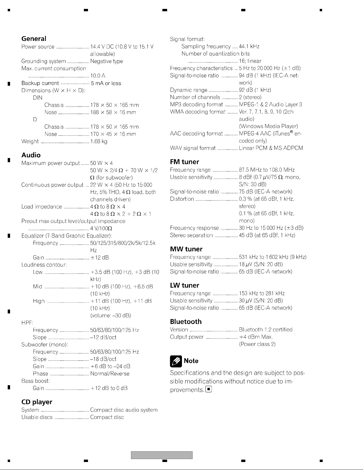
1. SPECIFICATIONS
A
B
C
D
E
F
6
1234
DEH-P85BT/XN/EW5
Page 7

5 678
A
B
C
D
E
56
DEH-P85BT/XN/EW5
F
7
8
7
Page 8
1234
N
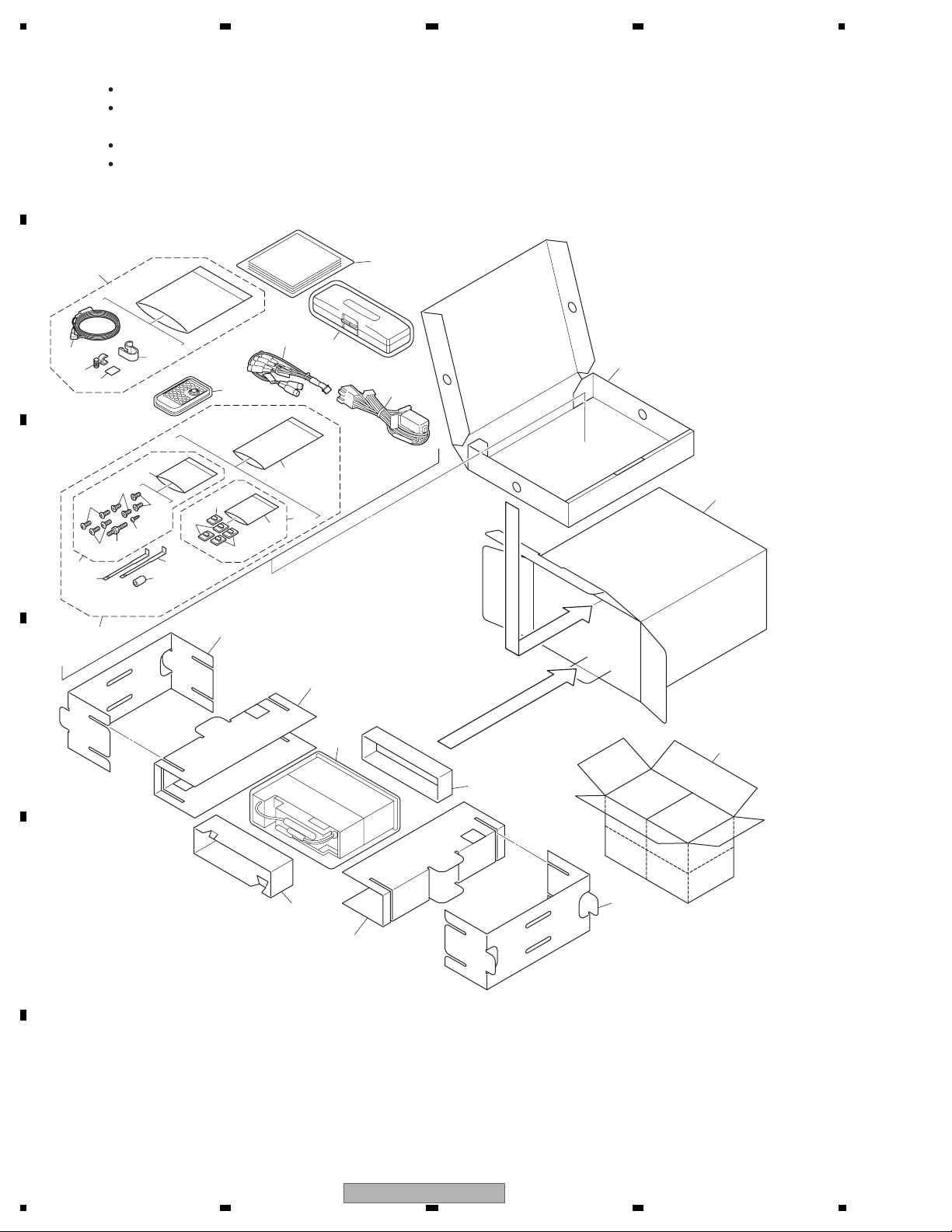
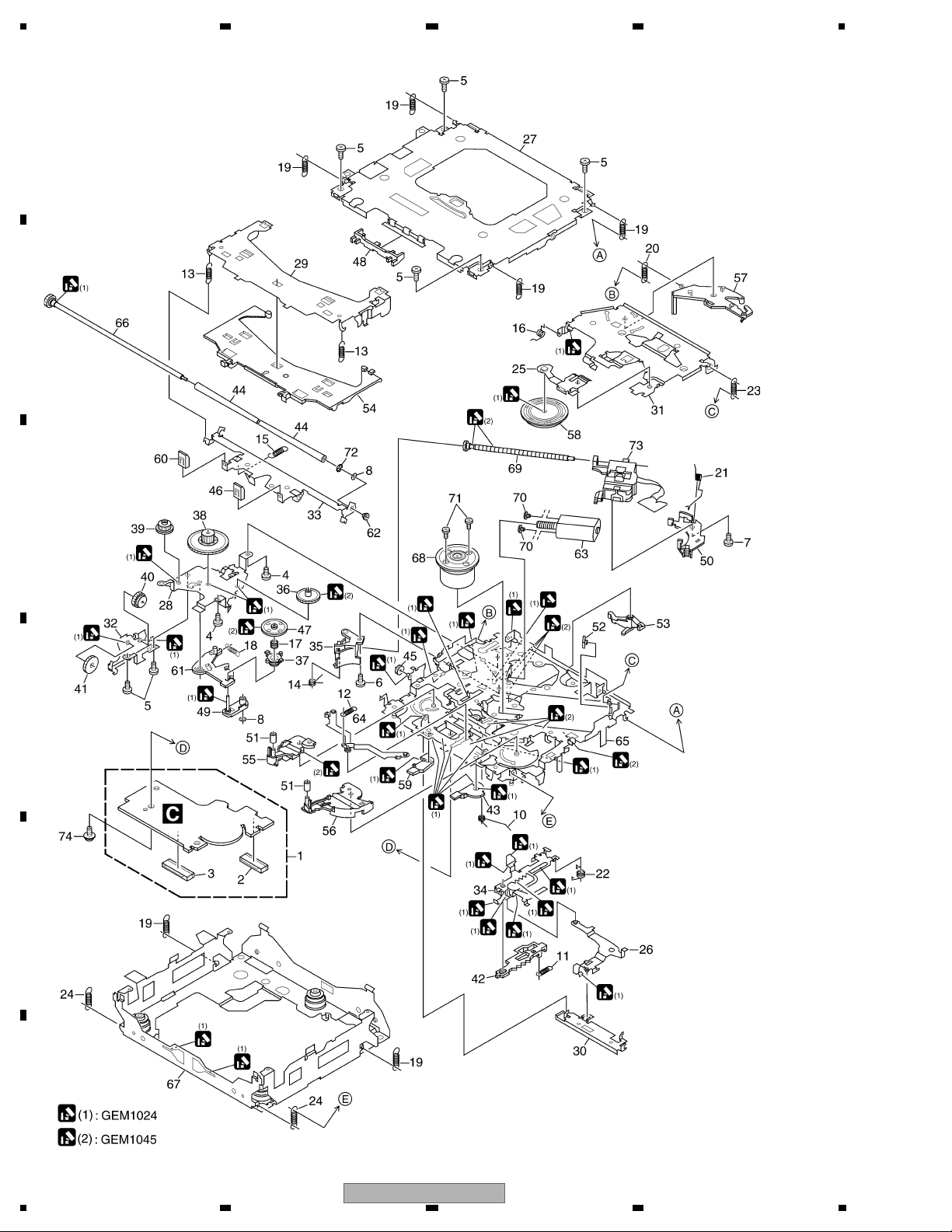
2. EXPLODED VIEWS AND PARTS LIST
OTES : Parts marked by " * " are generally unavailable because they are not in our Master Spare Parts List.
The > mark found on some component parts indicates the importance of the safety factor of the part.
A
Therefore, when replacing, be sure to use parts of identical designation.
Screw adjacent to mark on the product are used for disassembly.
For the applying amount of lubricants or glue, follow the instructions in this manual.
(In the case of no amount instructions,apply as you think it appropriate.)
2.1 PACKING
""
23
B
1
27
25
26
12
C
12
7
14
3
10
8
11
24
28
9
10
14
15
5
5
20
6
5
29
13
4
19
30
16
2
17
D
31
22
E
F
21
19
20
18
8
1234
DEH-P85BT/XN/EW5
Page 9
5 678
PACKING SECTION PARTS LIST
Mark No. Description Part No.
1 Cord Assy CDE8147
2 Cord Assy CDP1008
* 3 Accessory Assy CEA7537
4 Cord Clamper Assy CEA4636
* 5 Clamper CNV8262
* 6 Polyethylene Bag E36-615
7 Screw Assy CEA5322
8 Screw CBA1650
* 9 Polyethylene Bag CEG-127
10 Screw CRZ50P090FTC
11 Screw JPZ20P060FTB
12 Screw TRZ50P080FTC
* 13 Polyethylene Bag CEG1160
14 Handle CND3707
15 Bush CNV3930
16 Sub Unit Box CHG5195
17 Unit Box CHG6113
18 Contain Box CHL6113
19 Protector CHP2797
20 Protector CHP2798
Owner's Manual,Installation Manual
No. Description Part No.
Mark
21 Protector CHP2812
22 Protector CHP3184
23 Microphone Assy CPM1064
24 Clip Holder CZN5471
25 Microphone Holder CZN5472
26 Cushion CZN5473
* 27 Microphone CZX5059
28 Remote Control Unit CXC7555
29 Case Assy XXA7417
30-1 Owner's Manual CRB2352
30-2 Owner's Manual CRD4201
30-3 Owner's Manual CRD4202
30-4 Owner's Manual CRD4203
30-5 Installation Manual CRD4208
* 30-6 Caution Card CRP1335
* 30-7 Warranty Card CRY1157
30-8 Polyethylene Bag CEG1116
31 Polyethylene Bag CEG1227
A
B
C
Part No. Language
CRB2352 Russian
CRD4201 English, Spanish
CRD4202 German, French
CRD4203
CRD4208 English, Spanish, German, French, Italian, Dutch, Russian
Italian, Dutch
D
E
56
DEH-P85BT/XN/EW5
F
7
8
9
Page 10
1234
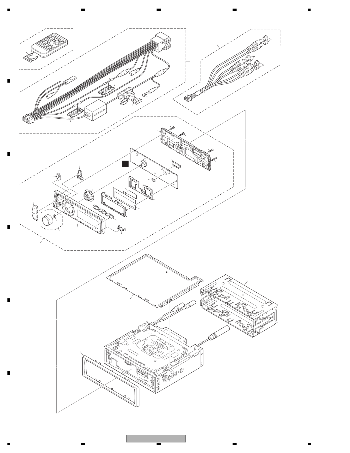
2.2 EXTERIOR(1)
A
31
1
2
32
2
3
2
7
6
5
7
B
6
4
12
15
12
12
18
29
16
C
25
28
20
BB
12
17
21
22
19
27
26
30
13
14
11
D
9
8
E
10
F
10
DEH-P85BT/XN/EW5
1234
Page 11

5 678
EXTERIOR(1) SECTION PARTS LIST
Mark No. Description Part No.
1 Cord Assy CDE8147
2 Cap CNV6727
3 Cord Assy CDP1008
> 4 Fuse(10 A) CEK1136
5 Cap CKX-003
6 Cap CNS1472
7 Resistor RS1/2PMF102J
8 Case CNB3447
9 Holder CND3598
10 Panel CNS8913
A
11 Detach Grille Assy CXC7494
12 Screw BPZ20P080FTB
13 Button(LIST/ATT/EQ/DISP/TA) CAI1469
14 Button(EJECT) CAI1155
15 Cover CNS8491
16 Lighting Conductor CNV9509
17 Connector(CN1961) CKS5545
18 Connector(CN1801) CKS5662
19 Holder CND3781
20 Double Sided Tape CNM8673
21 Holder CNV9435
22 OEL Unit MXS8260
23 •••••
24 •••••
25 Holder CNV9676
26 Knob Unit CXC7271
27 Spring XBL7005
28 Button Unit(SRC/BAND) CXC7558
29 Button Unit(PHONE) CXC7559
30 Sub Grille Assy CXC7499
31 Remote Control Unit CXC7555
32 Cover CZN5357
B
C
D
56
DEH-P85BT/XN/EW5
E
F
7
8
11
Page 12
1234
2.3 EXTERIOR(2)
94
43
EE
16
62
59
57
61
A
C
B
54
55
4
12
18
26
42
17
DD
15
14
15
1
10
6
9
34
91
44
32
14
33
92
37
36
28
D
27
24
20
E
21
29
30
AA
F
35
22
19
1
F
11
D
E
60
58
A
2
52
64
63
56
49
47
46
B
45
45
51
45
50
53
48
46
56
47
49
2
1
1
1
90
1
38
39
40
13
C
1
8
31
93
7
94
94
16
25
5
D
: GEM1024
: GEM1069
(2)
67
73
FF
75
82
66
67
74
3
89
78
E
3
89
86
66
A
85
66
72
89
87
88
71
81
70
67
80
B
23
68
(2)
69
84
65
F
12
1234
83
C
79
79
77
89
76
89
3
DEH-P85BT/XN/EW5
66
66
3
66
Page 13

5 678
EXTERIOR(2) SECTION PARTS LIST
Mark No. Description Part No.
1 Screw BSZ26P060FTC
2 Screw(M2.6 x 4) CBA1828
3 Screw(M2 x 2.5) CBA1924
4 Cord Assy CDE8051
5 Cable CDE8388
6 Earth Plate CND2171
7 Holder CND3606
8 Insulator CNM7682
9 Insulator CNM8790
10 Cushion CNM9126
11 Insulator CNM9936
12 Tuner Amp Unit CWN2341
13 Screw BMZ26P040FTC
14 Screw BMZ26P100FTC
15 Screw BMZ26P180FTC
16 Screw BSZ26P060FTC
17 Screw(M2.6 x 14) CBA1632
18 Antenna Cable(CN401) CDH1336
19 Clamper CEF1050
20 Plug(CN981) CKM1278
21 Connector(CN301) CKM1389
22 Plug(CN881) CKS-786
23 Connector(CN701) CKS3829
24 Connector(CN151) CKS4124
25 Connector(CN801) CKS4811
26 Connector(CN181) CKS4980
27 Connector(CN101) CKS5271
28 Connector(CN521) CKS5321
29 Connector(CN561) CKS5683
30 Holder(CN983) CNC5399
31 Holder CND3133
32 Holder CND3834
33 Heat Sink CNR1904
34 FM/AM Tuner Unit CWE1951
35 Holder CND1054
36 Bluetooth Unit CWN2339
37 Connector(CN76) CKS5320
38 Connector(CN1) CKS5749
39 Shield CND3134
40 Sheet CNM9598
41 •••••
42 Fan Motor CXM1288
43 7P FFC Connector (CN522) VKN1299
44 ZH Connector 2P (CN891) VKN1928
45 Screw(M2 x 2) CBA1871
46 Screw(M2 x 2) CBA1935
47 Spring CBH2530
48 Connector CKS5273
49 Arm CNV6962
No. Description Part No.
Mark
50 Guide CNV6967
51 Guide CNV8048
52 Case Unit CXC5695
53 Screw(M2 x 3.5) XBA7002
54 Holder XNC7019
55 Flexible PCB XNP7026
56 Screw(M2 x 3.5) CBA2030
57 Cord Assy CDE8474
58 Earth Plate CND3138
59 Holder CND3139
60 Insulator CNN1499
61 Antenna Unit CWN2634
62 Connector(ANT1102) CKS5749
63 BT Antenna(ANT1101) CWX3132
64 Panel Unit CXC5696
65 Drive Unit CXC8074
66 Screw BMZ26P040FTC
67 Screw(M2 x 2) CBA1871
68 Cord CDE7392
69 Gear CNV7752
70 Gear CNV7753
71 Gear CNV7754
72 Gear CNV7755
73 Switch Unit CWS1389
74 Switch CSN1051
75 Spring Switch CSN1052
76 Arm Unit CXC2199
77 Arm Unit CXC6623
78 Arm Unit CXC6624
79 Screw JFZ20P020FTC
80 Spring XBL7003
81 Holder XNC7017
82 Insulator XNM7119
83 Holder Unit XXA7399
84 Motor Unit(M3) XXA7400
85 Holder Unit XXA7401
86 Arm Unit XXA7403
87 Gear Unit XXA7424
88 Shaft XLA7001
89 Washer YE15FTC
90 CD Mechanism Module(S10.5) CXK5763
91 Screw ISS26P055FTC
92 IC(IC351) PAL007C
93 IC(IC911) NJM2388F84
94 Transistor(Q453,Q751,Q901) 2SD2396
A
B
C
D
E
F
56
DEH-P85BT/XN/EW5
7
8
13
Page 14
1234
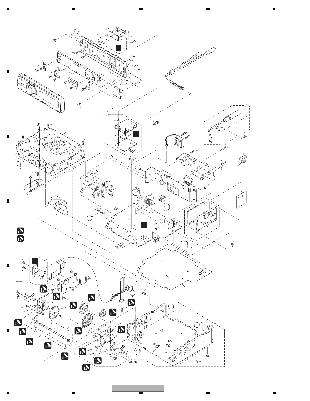
2.4 CD MECHANISM MODULE
A
B
C
D
E
F
14
1234
DEH-P85BT/XN/EW5
Page 15

5 678
CD MECHANISM MODULE SECTION PARTS LIST
Mark No. Description Part No.
1 CD Core Unit(S10.5COMP2) CWX3514
2 Connector(CN101) CKS4182
3 Connector(CN701) CKS4808
4 Screw BMZ20P025FTC
5 Screw BSZ20P040FTC
6 Screw(M2 x 3) CBA1511
7 Screw(M2 x 4) CBA1835
8 Washer CBF1038
9 •••••
10 Spring CBH2609
11 Spring CBH2612
12 Spring CBH2614
13 Spring CBH2616
14 Spring CBH2617
15 Spring CBH2620
16 Spring CBH2855
17 Spring CBH2937
18 Spring CBH2735
19 Spring CBH2854
20 Spring CBH2642
21 Spring CBH2856
22 Spring CBH2857
23 Spring CBH2860
24 Spring CBH2861
25 Spring CBL1686
26 Arm CND1909
27 Frame CND2582
28 Bracket CND2583
29 Arm CND2584
30 Lever CND2585
No. Description Part No.
Mark
50 Rack CNV8342
51 Roller CNV8343
52 Holder CNV8344
53 Arm CNV8345
54 Guide CNV8347
55 Arm CNV8348
56 Arm CNV8349
57 Arm CNV8350
58 Clamper CNV8365
59 Arm CNV8386
60 Guide CNV8396
61 Arm CNV8413
62 Collar CNV8938
63 Motor Unit(M2) CXC4026
64 Arm Unit CXC4027
65 Chassis Unit CXC4028
66 Gear Unit CXC4029
67 Frame Unit CXC4031
68 Motor Unit(M1) CXC7134
69 Screw Unit CXC6359
70 Screw JFZ20P020FTC
71 Screw JGZ17P022FTC
72 Washer YE20FTC
73 Pickup Unit(P10.5)(Service) CXX1942
74 Screw IMS26P030FTC
A
B
C
D
31 Arm CND2586
32 Bracket CND2587
33 Arm CND2588
34 Lever CND2589
35 Holder CNV7201
36 Gear CNV7207
37 Gear CNV7208
38 Gear CNV7209
39 Gear CNV7210
40 Gear CNV7211
41 Gear CNV7212
42 Rack CNV7214
43 Arm CNV7216
44 Roller CNV7218
45 Gear CNV7219
46 Guide CNV7361
47 Gear CNV7595
48 Guide CNV7799
49 Arm CNV7805
56
DEH-P85BT/XN/EW5
E
F
7
8
15
Page 16
1234
I
0
U
3
U
W
E
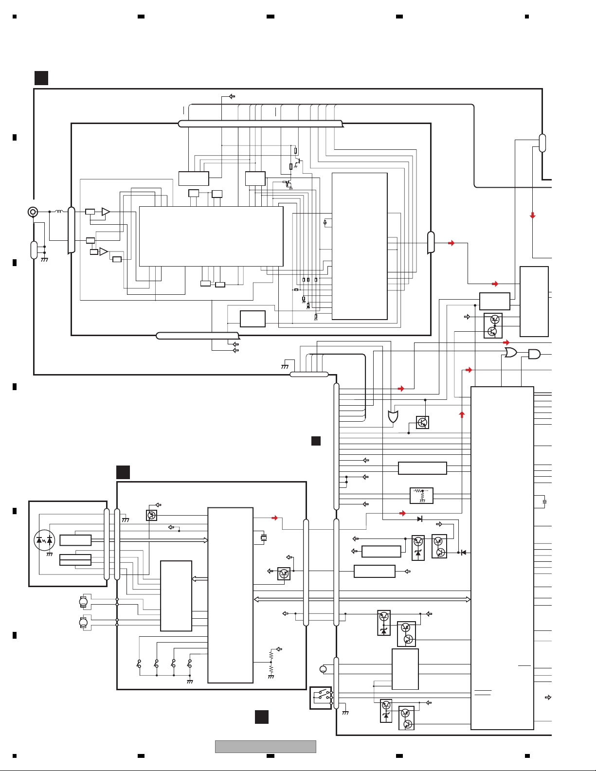
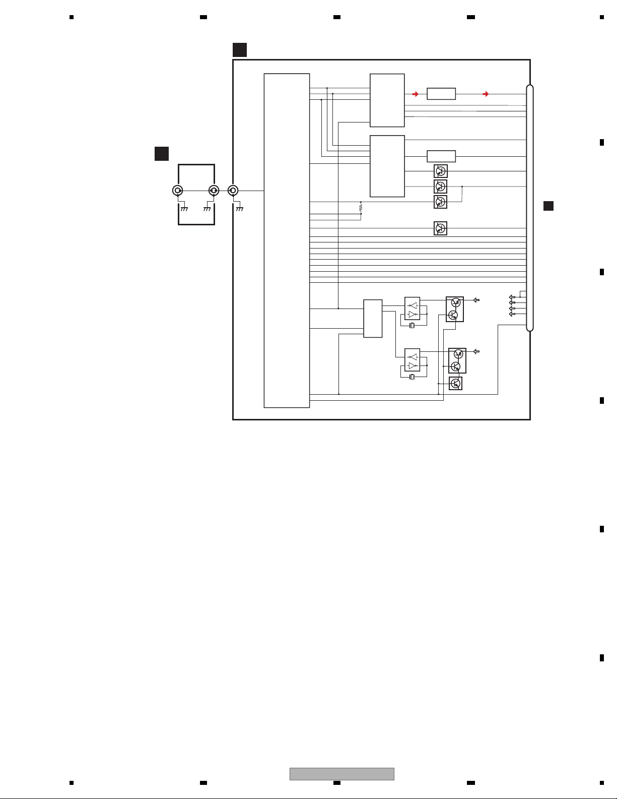
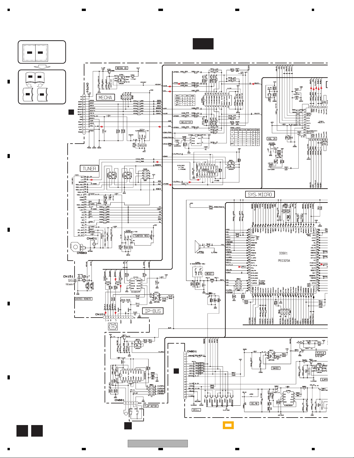
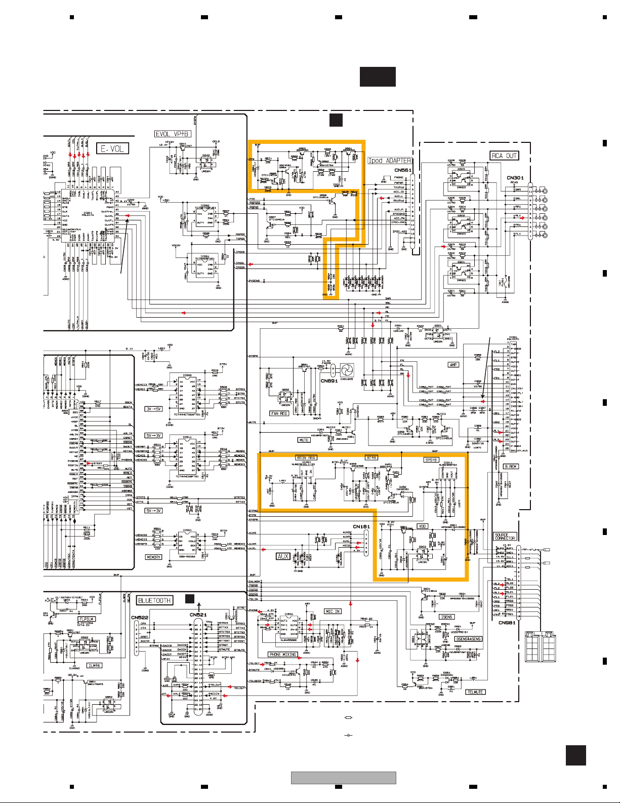
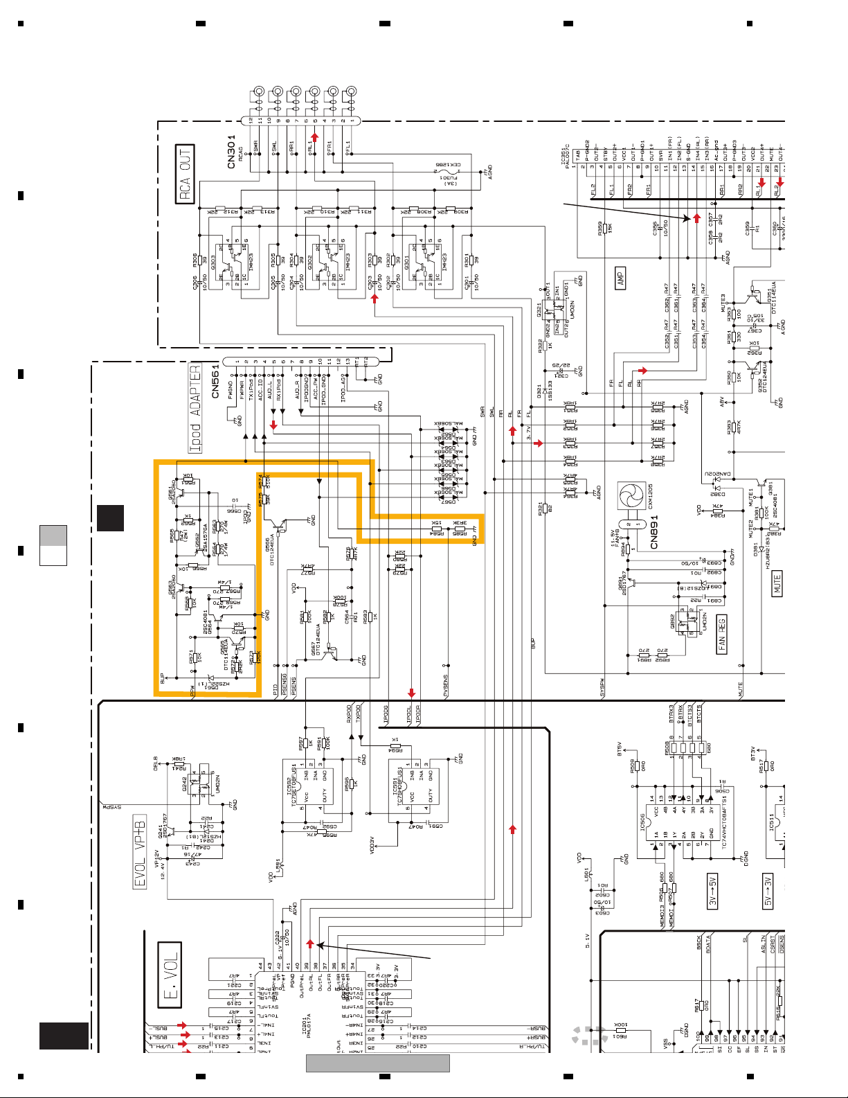
3. BLOCK DIAGRAM AND SCHEMATIC DIAGRAM
3.1 BLOCK DIAGRAM
A
A
TUNER AMP UNIT
VDD
LDET
LDET
DI
DO
RDS_CK
RDS_DATA
RDS_HSLK
RDS_LOCK
FM/AM TUNER UNIT
SL
CK
DO
CE2
76 13 5 1098 11 14 18192021
NC
CE2
ROM_VDD
CE1
DI
SL
CK
CE1
CN181
4
A
3
B
CN401
1
2,3
2
1
CN983
C
D
PICKUP UNIT
(P10.5)(SERVICE)
LASER
DIODE
E
F
MONITOR
DIODE
LOAD/
AM ANT
1
FM ANT
3
HOLOGRAM
UNIT
FOCUS ACT.
TRACKING ACT.
SPINDLE
MOTOR
CARRIAGE
MOTOR
IC262
TC4066BFT
IN/OUT1
IN/OUT2
CONT1
CONT2
2
1
TC7SET08F
75
EMUTE
SACLK
SAOUT
MUTE
SYSPW
MEMDI
MEMCS
MEMCK
XIN
XOUT
FLPILM
TXPOD
RXPOD
PSENS
PID
PPW
ILMPW
ROT0
ROT1
SWVDD
RESET
DSENS
DPDT
KYDT
OELPW
AUXL
OUT/IN1
OUT/IN2
IC263
57
58
90
85
1
4
18
19
3
5
13
11
40
22
20
35
21
9
87
37
36
39
38
10
91
29
30
BUP
42
R
2
4
2
VDD_3.3
IC201
3.3V
VDSENS
3.3V 2.5V
TUN3V
A8V
LOUT
XTAL
/XTAL
/PUEN
/RESET
IC 5
←
5V 3.3V
IC 4
←
55
50
52
39
16
11
VCC
F
BRST,BRXEN,BSRQ
BDATA,BSCK
2.5V
ORX
BTPW2
7
6
1
CN701
LOUT
X201
16.93MHz
13
VDD
Q102
VDD
9
/RESET
8
VD
2
VD
1
VD
SWITCH UNIT
OTX
2
D
CN76
BOOTE
ORST
54
M
FLAP
MOTOR
CN522
RDS DECODER
CN521
AVL
24
MICIN
17
TELOUT
15
HFAV
32
ORX
40
OTX
39
BOOTE
36
BTRST
6
BTMUTE
7
BTTEST
5
DACCS
35
DACDT
33
DACCK
34
11
BTCTS3
3
BTRX3
1
8
9
10
BTTX3
2
BTRTS3
4
12
CN701
LOUT
3
BT5V
BT3V
VDD
7
RESET
8
VD
14
15
CN881
FLM02
4
FLM01
5
FLOP
2
FLCL
3
1
IC 2
2.5V
DET, FM MPX,
BT3V REGULATOR
3
NJM2391DL1-33
3
NJM2885DL1-33
IC711
MUTE
Q541
BT5V
BT3V
3V 5V
9
IC506(1/2)
12
TC74VHCT08AFTS1
5V 3V
A8V
Q453
1
IC461
1
VDD
BRST,BRXEN,BSRQ,BDATA,BSCK
MECHA VD
Q751
Q752
IC881
BA6288FS
OUT2 RIN
VM
VCC
11
63
FINOUT1
Q872
Q871
14
4
5
Lch
23
←
←
BUP
BT+B
Q452
BUP
AUTO FLAP
MOTOR DRIVE
BUP
8
11
Q451
A8V
PHONE MIXING
7
2
NJM4558MD
24
PEE2
43
EVOLSW3
65
BTRST
66
BTMUTE
63
BTTEST
54
DACCS
55
DACDT
56
DACCK
61
BTCTS
34
BTRX
33
BTTX
68
BTRTS
CONTROLLER
64
BTPW
92
CDRST
59
VDCONT
52
FLPCLS
53
FLPOPN
50
FOPNSW
51
FCLSSW
49
FLPPW
IC531
ROMCK
SYSTEM
IC601(1/2)
PEG329A
74
Q261
1TUNL
6
4
1
13
5
ROMDATA
MEMWP
MEMDO
PVSENS
IC 3 EEPROM
5.0V
OSC
LPF
FMRF
ATT
IC 1
OSCGND
CD
CLCONT
CONT
3.3V
MIXER, IF AMP
T51
DGND
AUDIOGNDNCVCC
RF-AMP, CD DECODER,
MP3/WMA DECODER,
141
142
133
TD,FD
SD,MD
22
5
LOEJ
21
43
9
41
8
7
6
9
S901
HOME
CF52
DIGITAL SERVO /
DATA PROCESSOR
LD
PD
REFOUT
PE5547A
LOEJ
CLCONT
CONT
12EJ
8EJ
DSCSNS
HOME
ATT
FMRF
RF adj
ANT adj
RFGND
212 1522 16 4 17
CD CORE UNIT(S10.5COMP2)
C
Q101
S905
8EJ
12
11
14
13
16
15
18
17
REFO
VDD
AC,BD,F,E
DRIVER
IC301
BA5839FP
FOM
FOP
TOP
TOM
SOP
SOM
LCOP
LCOM
S903
DSCSNS
CN101
LD-
15
15
MD
5
5
VREF
88
FOM
FOM
33
FOP
FOP
2
2
TOP
TOP
1
1
TOM
TOM
44
LD+
14
14
M
M
S904
12EJ
16
DEH-P85BT/XN/EW5
1234
Page 17
5 678
A
E MIXING
531
558MD
Q261
74
ROMCK
TEM
OLLER
1(1/2)
329A
CN181
IC262
TC4066BFT
1
IN/OUT1
6
4
1
IN/OUT2
13
CONT1
5
CONT2
2
1
TC7SET08FUS1
75
ROMDATA
EMUTE
SACLK
SAOUT
MUTE
SYSPW
MEMDI
MEMCS
MEMWP
MEMDO
MEMCK
XIN
XOUT
FLPILM
TXPOD
RXPOD
PSENS
PID
PPW
PVSENS
ILMPW
ROT0
ROT1
SWVDD
RESET
DSENS
DPDT
KYDT
OELPW
AUXL
OUT/IN1
OUT/IN2
IC263
57
58
90
85
1
4
18
19
3
5
13
11
40
22
20
35
21
9
87
37
36
39
38
10
91
29
30
BUP
42
4
AUX
3
REMOTE
2
3
4
20.000MHz
IP-BUS
WIRED
X601
TXPOD
RXPOD
PSENS
PVSENS
VDD
SELECTOR
18
20
16
9
PID
PPW
Q852
CN101
CN151
3
2
1
IC261
BA3131FS
+IN2B
14
OUT2
15
-IN2C
+IN2A
+IN2C
SW2
VST,VCK,VDT
3V 5V
3
IC506(2/2)
TC74VHCT08AFTS1
4
5V 3V
1
IC511
12
TC74VHC08FTS1
9
FLPILM
Q831
BUP
SWVDD
Q841
1
Q651
OEL+B
Q851
DC-DC CONVERTER
BUSBUS+
BUSL-
BUSL+
MIC251
BUSL+
BUSL-
SOUTL
TU/PH_L
CDL
VDD
6
3
11
8
Q101
IP-BUS DRIVER
5
HA12241FP
CE2
CE1
DO
DI
CK
SL
RDS_CK
RDS_HSLK
RDS_DATA
RDS_LOCK
LDET
VR251
1
8
5
1
7
11
←
←
ILM+B
Q822
RESET
IC651
S-80835CNMC-B8U
IC851
6
NJM2360M
IC101
8
1
Q401
Q402
20
22
7
6
10
8
9
2
SO
1
CS
3
W#
5
SI
6
SCK
Q821
2
SYSTEM
CONTROLLER
IC601(2/2)
PEG329A
IC201
PML017A
Mute
SACLK
14
13
12
BUZZER
26
PEE
DALMON
OutPreL
OutFL
OutRL
SAOut
43
BUP
80
ASENBO
28
1
TX
26
27
RX
79
IPPW
2
KEYD
89
KEYAD
69
TUNPCE2
70
TUNPCE1
47
TUNPDO
46
TUNPDI
48
TUNPCK
95
SL
16
RCK
82
RDS57K/MODEL1
83
RDT/MODEL0
84
RDSLK
17
LDET
93
ASLIN
ELECTRONIC VOLUME/
SOURCE SELECTOR
NoiseDetOut
MicIn
IN4L+
IN4L-
IN1L
IN3L
IN2L
MEMORY
IC501
S99-50084
CN801
IL+B
13
ROT0
8
ROT1
9
SWVDD
10
VDD
RESET
5
DSENS
2
DPDT
6
KYDT
7
OEL+B
15
OELB
SP601
BSENS
ASENS
ISENS
TELIN
VP
B
CN1801
40
38
39
Q241
RL
67
73
72
81
8
EVOL VP+B
Q242
SWL
FL
BUP
BACKUP SENSE
ACC SENSE
MUTE
Q352
MUTE
Q351
Q381
MUTE
OELB
TXPOD
RXPOD
PVSENS
PPW
BUP
Q321
Q921
TEL MUTE
12
14
VDD
Q951
POWER AMP
IN2(FL)
IN4(RL)
22
BUP
SYSPW
TC7SET08FUS1
Q565
Q931
ILM SENSE
IC351
PAL007C
STBYMUTE
4
IC592
Q567
VDD REGULATOR
Q901
Q902
6,20
VCC1,VCC2
5
OUT2+
3
OUT2-
21
OUT4+
23
OUT4-
25
Switch_out
BUP
SYS+B REGULATOR
2
A8V
3
TUN3V
TC7SH08FUS1
Q566
Q564
Q563
BUP
BUP
FAN REG
Q892
IC911
NJM2388F84
4
TUNER 3V
REGULATOR
IC431
NJM2391DL1-33
IC591
14
Q562
Q891
Q561
Q302
Q303
Q301
1
1
SWL
RL
FL
CN301
CN981
BUP1
ACC1
TEL1
GND1
FL21
FL22
RL21
RL22
BRE1
CN891
BUP
CN561
AUD_LIPODL
TXiPod41
RXiPod
ACC-PWPSENS
ACC-IDPID
FWPWR
ILL1
A8V
5
9
1
1
5
3
8
2
SOURCE
CONNECTOR
12
10
11
9
4
2
FAN
1
5
3
6
iPod
10
ADAPTER
4
2
RCA OUT
B
C
D
E
F
56
DEH-P85BT/XN/EW5
7
8
17
Page 18
1234
A
B
A
CN801
B
KEYBOARD UNIT
CN1801
IL+B
12
ROT0
7
ROT1
8
SWVDD
9
REMOTE CONTROL
OPT IN
DPDT
5
KYDT
6
DSENS
1
14
4
RESET
S1801
RESET
SENSOR
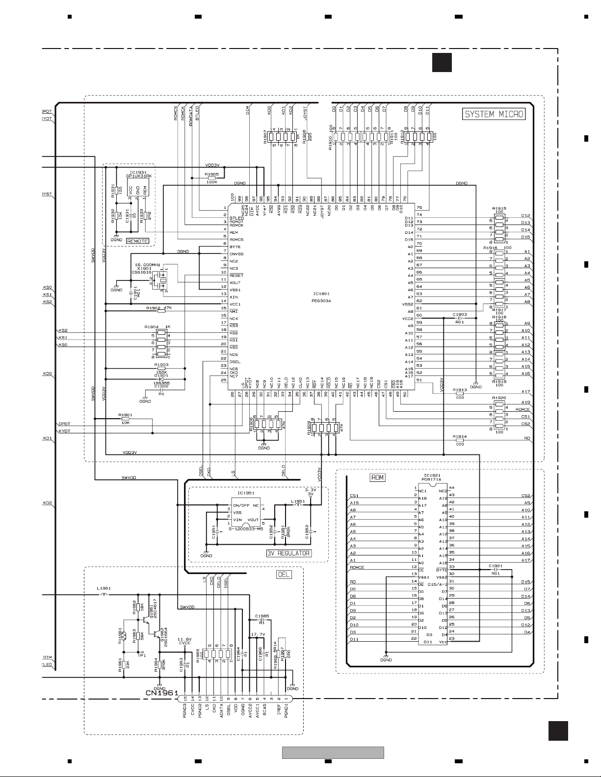
IC1931
GP1UX31RK
SWVDD
OEL+B
3
1
3V REGULATOR
1,3
IC1951
S-1200B33-M5
ROTARY COMMANDER
S1811
5
ROM
CE
23
A18
VCC
33
A19
BYTE
OE
IC1921
PD8171A
JOYST
12
43
14
ADDRESS
88
60
14
97
96
4
27
28
48
2
47
46
42
DATA
KEY MATRIX
S1831-S1839
IC1901
PEG303A
KD0-2,KS0-2
KEY/OEL CONTROLLER
JOYST
VCC2
VCC1
AVCC
Vref
REM
DPDT
KYDT
CSO
CS1
CS2
RD
BTLED
XOUT
CLK0
OELD
DSEL
(ILLUMINATION)
BT IND
Q1851
SWVDD
1
98
DIM
13
XIN
X1901
11
16MHz
26
LS
24
CKD
35
33
22
OEL+B
Q1852
Q1961
Q1834
Q1962
Q1831-Q1833
SWVDD
SWVDD
OEL+B
CN1961
CKD
ADATA
DSEL
VDD
AVCC 1
AVCC 2
CVCC
LS
12
11
10
9
8
OEL UNIT
5
6
14
C
D
E
F
18
DEH-P85BT/XN/EW5
1234
Page 19
5 678
D
BLUETOOTH UNIT
E
ANTENNA
ANTENNA UNIT
ANT1101
ANT1102
CN1
1
2,3
BLUETOOTH MODULE
SIOF_TXD
SIOF_SCK
SIOF_SYNC
Y1
SIOF_RXD
A5
RF_I/O
RESETP
REG_OUT
VCC_RF
SIOF_SS2
SCIF1_CTS
SCIF1_RTS
SCIF1_RXD
SCIF1_TXD
SCIF0_RXD
SCIF0_TXD
BOOT_E
SCIF0_CTS
SCIF0_RTS
SIOF_MCLK
SCO_CLK_OUT
SIOF_SS1
PTB1
DATAO
BCK
LRCK
MCK
N2
DATAI
Q2
G8
G9
P1
I1
I2
H2
H3
E2
E3
Q1
F1
F2
O1
MCK
L1
HFMCK
HFAV
O3
T3
DAC
IC56
PCM1742KE
2N3
DATA
1N1
BCKIN
3O2
LRCKIN
16
MCLK
CODEC
3
BCLK
4
DR
5
FS
2
DX
IC36
AK2301A
CLOCK SELECT
IC21
TC74VHC02FTS1
11
4A
4
2Y
12
4B
2
1A
3
1B
Vout L
MD
MC
ML
GSR
VFTN
MUTEN
RSTN
TC7PAU04FU
6
3
X21 11.2896MHz
TC7PAU04FU
6
3
X22 12.288MHz
13
14
15
7
15
23
22
OSC
IC22
OSC
IC23
VCC
VCC
HFAV
FSCHG
37
NJM4558V
5
AN6123MS
Q37
Q36
Q1
Q2
5
1
4
5
1
4
LPF
IC66
ALC
IC51
A
B
BT3V
BT3V
D3V
D5V
A8V
CN76
AUDIO L
DACDT
DACCK
DACCS
TELOUT
MICIN
BTMUTE
BTRST
BTTEST
BTRTS
BTCTS
BTTX
BTRX
ORX
OTX
BOOTE
OCTS
ORTS
HFAV
24
33
34
35
15
17
7
6
A
CN521
5
4
3
2
1
40
39
36
38
37
8
9
10
11
12
32
1,2
3
Q21
C
Q23
BT3V
Q22
D
E
F
56
DEH-P85BT/XN/EW5
7
8
19
Page 20
1234
A-a
A-b
A-a
A-b
A-b
A-a
h
h
3
3
-
T
B
v
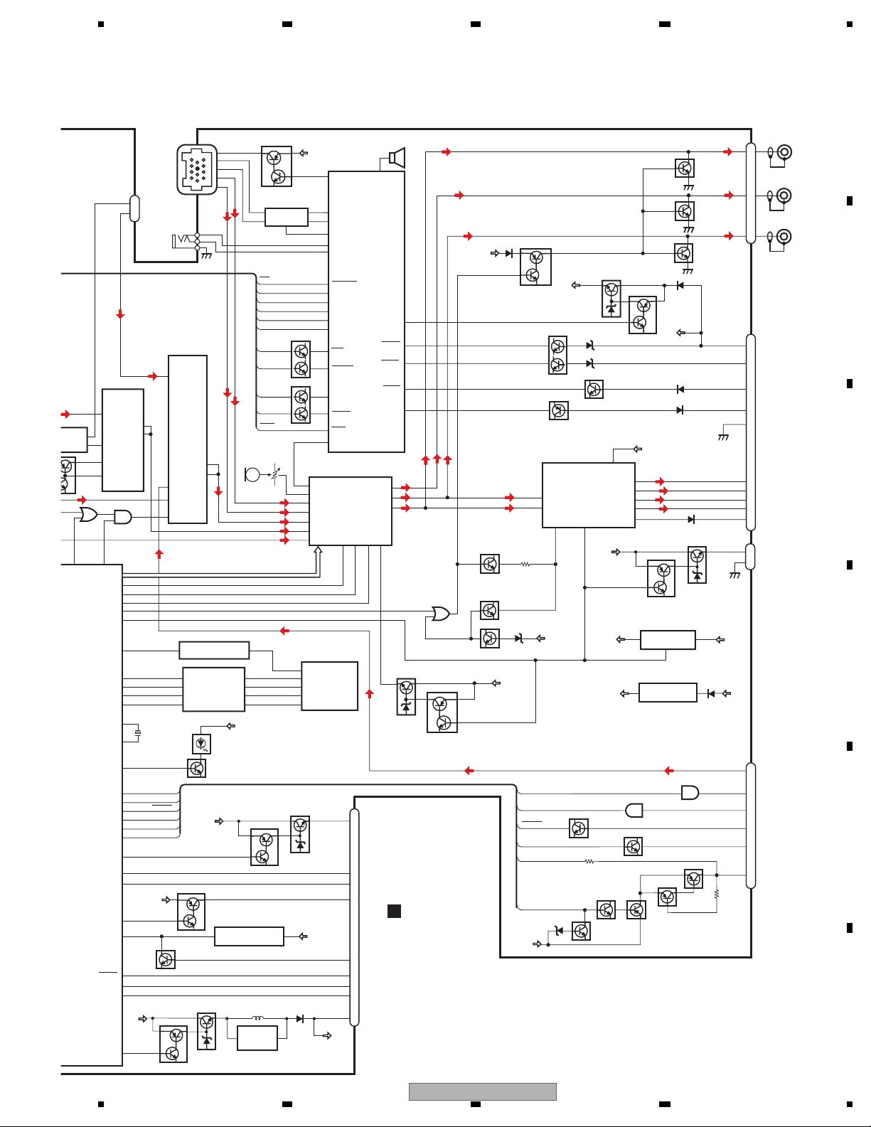
3.2 OVERALL CONNECTION DIAGRAM(GUIDE PAGE)
Note: When ordering service parts, be sure to refer to " EXPLODED VIEWS AND PARTS LIST" or
"ELECTRICAL PARTS LIST".
A
A-a
A-a
A-a
A-b
A-b
A-b
Large size
SCH diagram
Guide page
Detailed page
+2.2dBs
+3.01dBs
(ipod video:0dB play)
+1.3dBs
A-a
B
C
C
CN701
(0dB play)
+0.6dBs
FM(30%):-20dBs
AM(30%):-20dBs
FM(
AM(
IP
B
ipod(
FM/AM TUNER UNIT
(0dB play)
D
+2.2dBs
E
F
A F
20
B
CN1801
M
M3
FLAP MOTOR
XXA7400
1234
CSN1052
S2 CLOSE
CSN1051
S1 OPEN
SWITCH UNIT
F
DEH-P85BT/XN/EW5
: The power supply is shown with the marked box.
T
T
Page 21
5 678
FM(30%): +3.1dBs
AM(30%): +3.1dBs
IP-BUS: +14.3dBs
CD: +13.7dBs
BT TEL: +13.1dBs
BT AV:+14.11dBs
AUX: +14.3dBs
ipod(video): +14.4dBs
A-b
TUNER AMP UNIT
A
FAN
>
FM(30%): +25.1dBs
AM(30%): +25.1dBs
IP-BUS: +36.3dBs
CD: +35.7dBs
BT TEL: +35.1dBs
BT AV:+36.11dBs
AUX: +36.3dBs
ipod(video): +36.4dBs
A
B
C
CN76
D
-5dBs
The > mark found on some component parts indicates the importance of the safety factor of the part.
Therefore, when replacing, be sure to use parts of identical designation.
NOTE :
Symbol indicates a resistor.
No differentiation is made between chip resistors and
discrete resistors.
Symbol indicates a capacitor.
No differentiation is made between chip capacitors and
discrete capacitors.
1K(1/2W)
1K(1/2W)
Decimal points for resistor
and capacitor fixed values
are expressed as :
2.2
t
2R2
0.022
t
R022
CEK1136
BACK
UP
ILL
GND
>
10A
B.REM
D
B.UP
GND
ILL
ACC
TEL
RL-
FL-
RL+
FL+
RR-
FR-
RR+
FR+
RR
RR
+
FR
FR
+
-
B.
FL
FL
REM
+
RL
RL
ACC
+
-
E
F
A
56
DEH-P85BT/XN/EW5
7
8
21
Page 22
1234
A
>
CD: +35.7dBs
AUX: +36.3dBs
BT AV:+36.11dBs
IP-BUS: +36.3dBs
BT TEL: +35.1dBs
FM(30%): +25.1dBs
AM(30%): +25.1dBs
B
ipod(video): +36.4dBs
C
TUNER AMP UNIT
FAN
A
A-a A-b
D
E
F
A-b
22
CD: +13.7dBs
AUX: +14.3dBs
BT AV:+14.11dBs
IP-BUS: +14.3dBs
BT TEL: +13.1dBs
FM(30%): +3.1dBs
AM(30%): +3.1dBs
ipod(video): +14.4dBs
1
DEH-P85BT/XN/EW5
1234
Page 23
5 678
+
+
+
+
RL
FL
FR
RR
-
-
-
-
RL
FL
FR
RR
B.
REM
ACC
UP
ILL
GND
BACK
R022
t
2R2
t
Decimal points for resistor
and capacitor fixed values
are expressed as :
2.2
0.022
A
>
B.UP
10A
CEK1136
GND
ILL
1K(1/2W)
B.REM
ACC
1K(1/2W)
FL-
RL-
TEL
FR-
RR-
FR+
RR+
FL+
RL+
B
CN76
D
-5dBs
Symbol indicates a resistor.
No differentiation is made between chip resistors and
discrete resistors.
Symbol indicates a capacitor.
NOTE :
C
No differentiation is made between chip capacitors and
discrete capacitors.
A-a A-b
D
E
2
DEH-P85BT/XN/EW5
56
The > mark found on some component parts indicates the importance of the safety factor of the part.
Therefore, when replacing, be sure to use parts of identical designation.
A-b
F
7
8
23
Page 24
A
+
+
4
B
A-b
1234
CD: +
AUX: +
BT AV:+1
IP-BUS: +
BT TEL: +
FM(30%):
AM(30%):
ipod(video): +
1
C
A-bA-a
(ipod video:0dB play)
D
E
+1.3dBs
+2.2dBs
+3.01dBs
(0dB play)
+0.6dBs
FM(30%):-20dBs
AM(30%):-20dBs
F
A-a
24
FM/AM TUNER UNIT
C
CN701
DEH-P85BT/XN/EW5
1234
Page 25
5 678
M
The > mTherefor
A
2
A-b
B
: The power supply is shown with the marked box.
+2.2dBs
(0dB play)
B
CN1801
M
M3
A-bA-a
CSN1051
S1 OPEN
CSN1052
S2 CLOSE
SWITCH UNIT
F
XXA7400
FLAP MOTOR
C
D
E
F
A-a
DEH-P85BT/XN/EW5
56
7
8
F
F
25
Page 26
1234
3.3 KEYBOARD UNIT
A
A
CN801
B
C
D
E
F
B
26
1234
DEH-P85BT/XN/EW5
Page 27
5 678
KEYBOARD UNIT
B
A
B
C
D
E
OEL UNIT
56
MXS8260
DEH-P85BT/XN/EW5
F
B
7
8
27
Page 28
1234
3.4 CD MECHANISM MODULE(GUIDE PAGE)
A
C-a
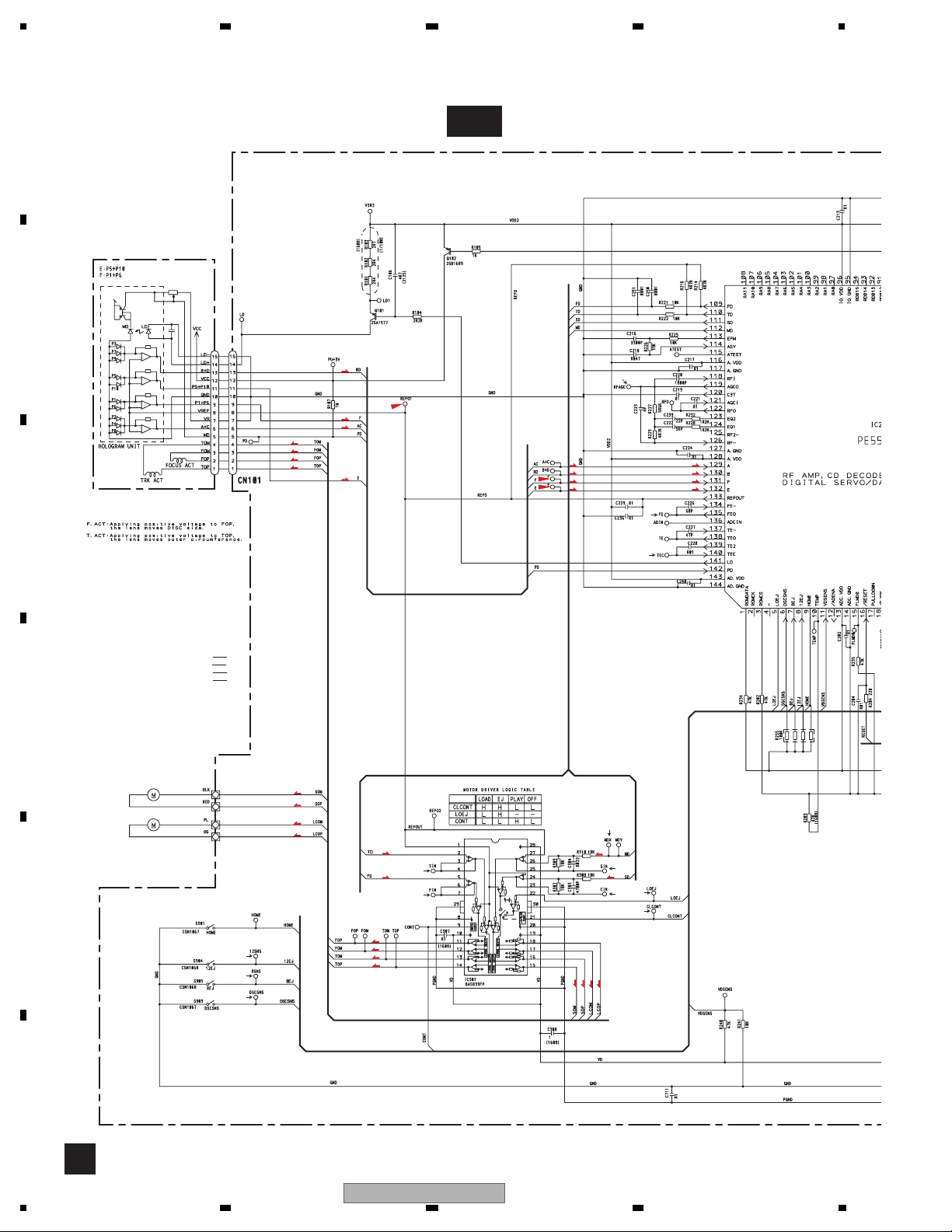
PICKUP UNIT(P10.5)(SERVICE)
B
F
T
F
T
F
F
T
T
F
F
T
T
C
%
F
F
T
T
#
@
SWITCHES:
CD CORE UNIT(S10.5COMP2)
S901:HOME SWITCH..........ON-OFF
S903:DSCSNS SWITCH......ON-OFF
S904:12EJ SWITCH.............ON-OFF
S905:8EJ SWITCH...............ON-OFF
The underlined indicates the switch position.
D
M1 CXC7134
SPINDLE MOTOR
M2 CXC4026
LOADING/CARRIAGE MOTOR
E
3
2
1
S
S
C
C
T
9
F
0
F
F
T
T
$
S
7
C
4
8
5
S
S
C
C
CD DRIVER
F
C
28
1234
DEH-P85BT/XN/EW5
Page 29
5 678
C-b
CD CORE UNIT(S10.5COMP2)
C
!
SIGNAL LINE
F
FOCUS SERVO LINE
T
TRACKING SERVO LINE
C
CARRIAGE SERVO LINE
S
SPINDLE SERVO LINE
A
B
C
D
A
CN701
6
E
&^
F
C
56
DEH-P85BT/XN/EW5
7
8
29
Page 30

1234
A
B
C
CD CORE UNIT(S10.5COMP2)
SIGNAL LINE
FOCUS SERVO LINE
TRACKING SERVO LINE
CARRIAGE SERVO LINE
F
T
C
SPINDLE SERVO LINE
S
C
C-a C-b
D
E
F
C-b
30
!
1
DEH-P85BT/XN/EW5
1234
Page 31

5 678
A
A
CN701
6
B
&^
C
C-a C-b
D
E
2 3
DEH-P85BT/XN/EW5
56
F
C-b
7
8
31
Page 32

A
S905:8EJ SWITCH ON-OFF
B
C-b
1234
1
FFT
T
#
%
FFT
T
C
C-bC-a
D
FFT
T
@
E
F
C-a
32
FFT
T
SWITCHES:
CD CORE UNIT(S10.5COMP2)
S901:HOME SWITCH..........ON-OFF
S903:DSCSNS SWITCH......ON-OFF
PICKUP UNIT(P10.5)(SERVICE)
S904:12EJ SWITCH.............ON-OFF
DEH-P85BT/XN/EW5
1234
Page 33

5 678
A
2 3
4
5
8
7
$
C
S
C
C
S
S
C-b
B
C
CD DRIVER
c-bC-a
9
0
F
T
S
S
C
C
F
F
T
T
3
2
1
D
E
SWITCHES:
CD CORE UNIT(S10.5COMP2)
S901:HOME SWITCH..........ON-OFF
S903:DSCSNS SWITCH......ON-OFF
S904:12EJ SWITCH.............ON-OFF
S905:8EJ SWITCH...............ON-OFF
The underlined indicates the switch position.
56
M1 CXC7134
SPINDLE MOTOR
M2 CXC4026
LOADING/CARRIAGE MOTOR
DEH-P85BT/XN/EW5
F
C-a
7
8
33
Page 34

1234
A
1DSCSNS
28SNS
312SNS
4LOEJ
12 cm CD Loading operation 12 cm CD Loading operation 8 cm CD Loading operation
Ref.:
GND
B
Mode:
Normal
7SIN
8CIN
9TIN
12 cm CD-DA setup operation after loading
C
Ref.:
REFO
5 V/div
5 V/div
5 V/div
5 V/div
1 V/div
500 mV/div
1 V/div
500 ms/div
1 s/div
2. Reference voltage REFO1(1.65 V)
1DSCSNS
5CLCONT
4LOEJ
6VD
Ref.:
GND
Mode:
Normal
RFOK(MONI_2)
!
7SIN
Ref.:
REFO
5 V/div
5 V/div
10 V/div
200 mV/div
2 V/div
2 V/div
500 ms/div5 V/div
500 ms/div0FIN
28SNS
312SNS
4LOEJ
Ref.:
GND
Mode:
Normal
#FE
Source On setup operation12 cm CD-DA Source On setup operation
Ref.:
REFO
5 V/div
5 V/div
5 V/div
5 V/div
500 mV/div
500 mV/div
500 ms/div1DSCSNS
200 ms/div@TE
- Wavef orms Note : 1. The encircled numbers denote measuring points in the circuit diagram.
Mode:
Normal
500 mV/div
0FIN
@TE
D
E
9TIN
CD-DA Play operation Spindle waveform during play operation Spindle waveform during play operation
Ref.:
REFO
Mode:
Normal
#FE
Focus Search waveform Track Open waveform 1 Track Jump waveform
500 mV/div
500 mV/div
500 mV/div
500 mV/div
500 mV/div
20 ms/div#FE
200 ms/div0FIN
Mode:
Normal
7SIN
Ref.:
REFO
Mode:
Normal
%RFAGC
2 V/div
500 mV/div
500 mV/div
500 mV/div
200 ms/div$MDX
2 ms/div@TE
Mode:
Normal
7SIN
(Wider)
Ref.:
REFO
Mode:
Normal
@TE
9TIN
2 V/div
500 mV/div
1 V/div
500 mV/div
500 mV/div
µs/div$MDX
5
500
µs/div%RFAGC
Ref.:
REFO
Mode:
TEST
F
34
1234
Ref.:
REFO
Mode:
TEST
DEH-P85BT/XN/EW5
Ref.:
REFO
Mode:
TEST
Page 35

5 678
A
1 V/div
@TE
9TIN
4 Tracks Jump waveform 10 Tracks Jump waveform 32 Tracks Jump waveform
Ref.:
REFO
Mode:
TEST
500 mV/div
500 mV/div
1 V/div
@TE
8CIN
7SIN
Search operation(Outter to Inner)
Ref.:
REFO
Mode:
Normal
1 V/div
1 V/div
2 V/div
500 µs/div%RFAGC
@TE
9TIN
Ref.:
REFO
Mode:
TEST
200 ms/div%RFAGC
&ROUT
Ref.:
AGND
Mode:
Normal
1 V/div
500 mV/div
500 mV/div
1 V/div
1 V/div
500 µs/div%RFAGC
200
@TE
9TIN
Ref.:
REFO
Mode:
TEST
µs/div^LOUT
28SNS
312SNS
4LOEJ
12 cm CD Eject operationAnalog audio waveform
Ref.:
GND
Mode:
Normal
1 V/div
500 mV/div
500 mV/div
5 V/div
5 V/div
5 V/div
5 V/div
2 ms/div%RFAGC
B
500 ms/div1DSCSNS
C
5 V/div
5 V/div
5 V/div
5 V/div
5CLCONT
4LOEJ
5 V/div
5 V/div
5 V/div
500 ms/div1DSCSNS
28SNS
312SNS
4LOEJ
12 cm CD Eject operation 8 cm CD Eject operation Black dot(800 µm) during play
Ref.:
GND
Mode:
Normal
Ref.:
GND
Mode:
Normal
500 ms/div1DSCSNS
9TIN
@TE
0FIN
Ref.:
REFO
Mode:
Normal
1 V/div
1 V/div
1 V/div
1 V/div
500
µs/div%RFAGC
D
E
F
56
DEH-P85BT/XN/EW5
7
8
35
Page 36

1234
3.5 BLUETOOTH UNIT, ANTENNA UNIT
A
B
C
D
E
F
D E
36
ANTENNA UNIT
E
DEH-P85BT/XN/EW5
1234
Page 37

5 678
BLUETOOTH UNIT
A
D
CN521
A
B
C
D
E
56
DEH-P85BT/XN/EW5
F
D
7
8
37
Page 38

1234
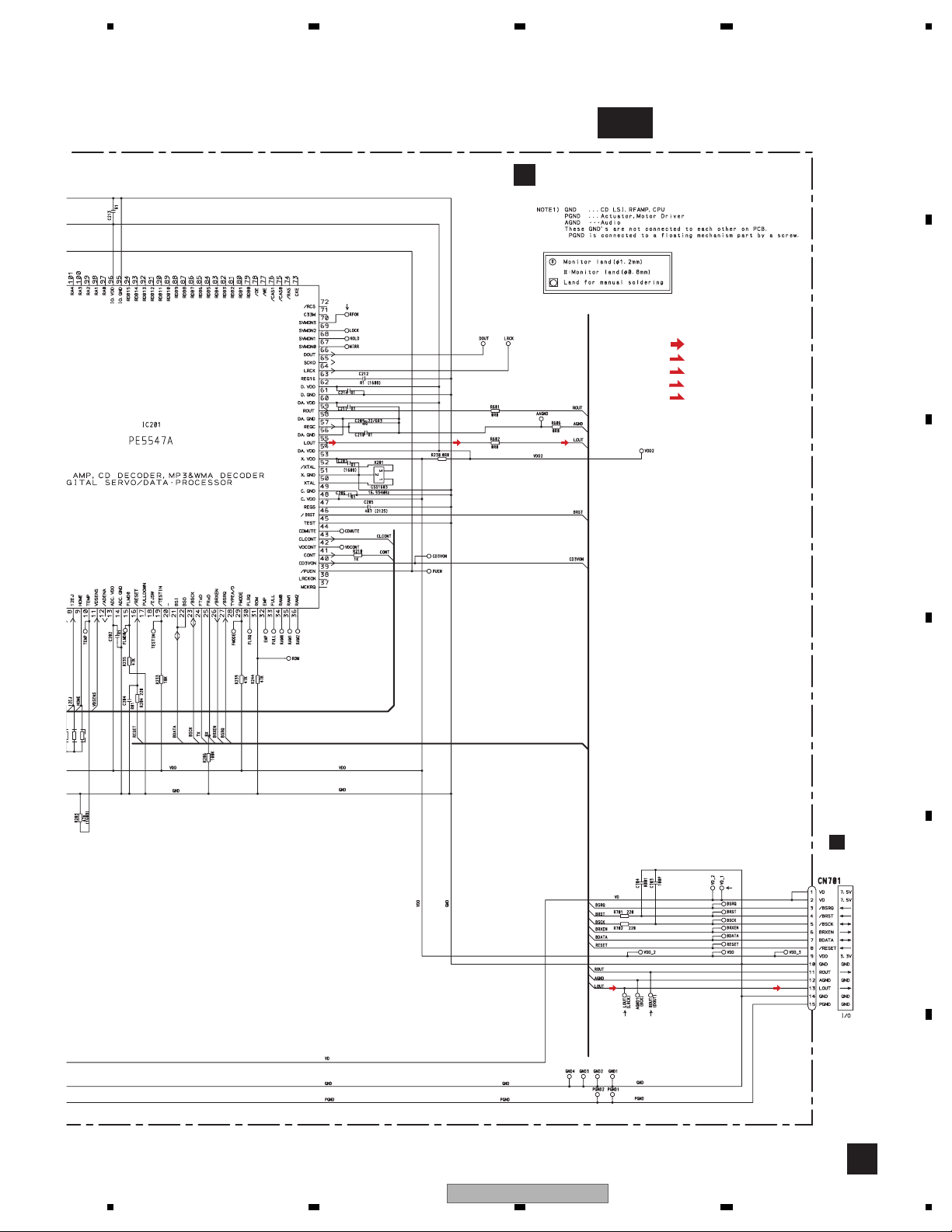
4. PCB CONNECTION DIAGRAM
4.1 TUNER AMP UNIT
A
B
C
NOTE FOR PCB DIAGRAMS
1.The parts mounted on this PCB
include all necessary parts for
several destination.
For further information for
respective destinations, be sure
to check with the schematic dia gra m.
2.Viewpoint of PCB diagrams
Connector
P.C.Board
Capacitor
Chip Part
SIDE A
SIDE B
TUNER AMP UNIT
A
FAN
150
140
130
120
110
100
90
IP-BUS
WIRED
REMOTE
CORD ASSY
15
16
1
2
80
AUX IN
70
D
D
CN76
60
50
40
E
30
20
10
Y
F
0
A
38
1234
DEH-P85BT/XN/EW5
10 20 30 40 50
X
60 70
Page 39

5 678
RCA OUTPUT
iPOD
ADAPTER
1
ANTENNA
FM/AM TUNER UNIT
SIDE A
A
B
C
70 80 90 100
FRONT
110 120
130 140 150
160
C
M3
B
CN701
F
CN1801
170
D
E
F
A
56
DEH-P85BT/XN/EW5
7
8
39
Page 40

1234
A
B
C
TUNER AMP UNIT
A
1
STEST
D
PCL1
E
F
170
160
130140150
110120
8090100
A
40
DEH-P85BT/XN/EW5
1234
Page 41

5 678
SIDE B
A
150
1
140
130
B
120
110
100
C
90
80
70
60
50
40
30
20
10
D
E
60708090
1020304050
DEH-P85BT/XN/EW5
56
Y
0
X
F
A
7
8
41
Page 42

1234
4.2 KEYBOARD UNIT
KEYBOARD UNIT
A
B
C
B
140 150 160
OEL
UNIT
SIDE A
90 100 110 120 130
LIST ATT EQ DISPLAY TA/NEWS RESET EJECT
D
60 70 80
MULTI-CONTROL
E
PHONE
BAND
10 20 30 40 50
F
B
42
1234
SOURCE
40
DEH-P85BT/XN/EW5
30
20
10
X
0
Y
Page 43

5 678
KEYBOARD UNIT
B
160 150 140 130 120
110 100 90
A
SIDE B
A
B
CN801
C
80 70 60 50 40
30 20 10
D
E
X
0
10
20
Y
56
DEH-P85BT/XN/EW5
30
F
40
B
7
8
43
Page 44

1234
4.3 CD CORE UNIT(S10.5COMP2)
CD CORE UNIT(S10.5COMP2)
A
B
C
C
A
CN701
PICKUP UNIT(P10.5)(SERVICE)
SIDE A
D
E
M2
LOADING
/CARRIAGE
MOTOR
M1
SPINDLE
MOTOR
F
44
C
DEH-P85BT/XN/EW5
1234
Page 45

5 678
CD CORE UNIT(S10.5COMP2)
C
SIDE B
A
B
C
D
E
F
56
DEH-P85BT/XN/EW5
C
7
8
45
Page 46

1234
4.4 BLUETOOTH UNIT
BLUETOOTH UNIT
A
B
C
D
40
30
A
CN521
SIDE A
20
D
10
E
Y
0
F
X
10 20 30
46
D
DEH-P85BT/XN/EW5
1234
Page 47

5 678
BLUETOOTH UNIT
D
SIDE B
A
B
40
C
30
30 20 10
ANT1102
E
20
10
D
E
Y
X
0
F
56
DEH-P85BT/XN/EW5
D
7
8
47
Page 48

1234
4.5 ANTENNA UNIT
ANTENNA UNIT
A
B
C
E
D
CN1
ANTENNA UNIT
E
SIDE BSIDE A
D
E
F
48
E
DEH-P85BT/XN/EW5
1234
Page 49

5 678
4.6 SWITCH UNIT
SWITCH UNIT
F
A
A
CN881
CLOSE
30 20 10
OPEN
X
20
10
B
Y
C
0
D
56
DEH-P85BT/XN/EW5
E
F
F
7
8
49
Page 50

1234
N
5. ELECTRICAL PARTS LIST
OTE:
A
Parts whose parts numbers are omitted are subject to being not supplied.
The part numbers shown below indicate chip components.
Chip Resistor
RS1/_S___J,RS1/__S___J
Chip Capacitor (except for CQS.....)
CKS....., CCS....., CSZS.....
The > mark found on some component parts indicates the importance of the safety factor of the part.
Therefore, when replacing, be sure to use parts of identical designation.
Meaning of the figures and others in the parentheses in the parts list.
B
Example) IC 301 is on the point (face A, 91 of x-axis, and 111 of y-axis) of the corresponding
PC board.
IC 301 (A, 91, 111) IC NJM2068V
Circuit Symbol and No. Part No.
Unit Number : CWN2341
Unit Name : Tuner Amp Unit
Unit Number :
Unit Name : Keyboard Unit
C
Unit Number : CWN2339
Unit Name : Bluetooth Unit
Unit Number : CWN2634
Unit Name : Antenna Unit
Unit Number: CWS1389
Unit Name : Switch Unit
Unit Number: CWX3514
D
Unit Name : CD Core
Unit(S10.5COMP2)
A
Unit Number : CWN2341
Unit Name : Tuner Amp Unit
MISCELLANEOUS
E
IC 101 (A,16,117) IC HA12241FP
IC 201 (A,103,87) IC PML017A
IC 261 (A,70,89) IC BA3131FS
IC 262 (A,72,71) IC TC4066BFT
IC 263 (A,72,79) L-MOS And Gate TC7SET08FUS1
IC 351 (A,86,135) IC PAL007C
IC 431 (B,155,83) IC NJM2391DL1-33
IC 461 (B,39,71) IC NJM2391DL1-33
IC 501 (A,112,37) IC S99-50084
IC 506 (A,99,35) IC TC74VHCT08AFTS1
F
IC 511 (A,106,37) IC TC74VHC08FTS1
IC 531 (B,55,48) IC NJM4558MD
IC 591 (A,130,104) IC TC7SH08FUS1
IC 592 (A,130,108) L-MOS And Gate TC7SET08FUS1
50
1234
Circuit Symbol and No. Part No.
IC 601 (A,126,58) IC PEG329A
IC 651 (A,123,81) IC S-80835CNMC-B8U
IC 711 (B,89,18) IC NJM2885DL1-33
IC 851 (A,33,22) IC NJM2360M
IC 881 (A,148,16) IC BA6288FS
IC 911 (A,15,79) IC NJM2388F84
Q 101 (A,25,116) Transistor UMF23N
Q 241 (B,87,99) Transistor 2SD1767
Q 242 (A,90,99) Transistor UMD2N
Q 261 (A,67,79) Transistor UMD2N
Q 301 (A,114,123) Transistor IMH23
Q 302 (A,114,118) Transistor IMH23
Q 303 (A,107,117) Transistor IMH23
Q 321 (A,108,123) Transistor UMD2N
Q 351 (A,105,125) Chip Transistor DTC114EUA
Q 352 (A,104,122) Chip Transistor DTC124EUA
Q 381 (A,101,125) Transistor 2SC4081
Q 401 (A,149,95) Transistor UMH1N
Q 402 (A,155,96) Transistor UMH1N
Q 451 (A,29,100) Transistor 2SB1243
Q 452 (A,35,103) Chip Transistor DTC114EUA
Q 453 (A,14,100) Transistor 2SD2396
Q 541 (B,56,37) Transistor DTC314TU
Q 561 (A,148,129) Transistor 2SA2060
Q 562 (A,144,122) Transistor 2SA1576A
Q 563 (A,128,121) Transistor 2SA2060
Q 564 (A,135,119) Transistor 2SC4081
Q 565 (A,135,121) Chip Transistor DTC114EUA
Q 566 (A,146,108) Chip Transistor DTC124EUA
Q 567 (A,142,102) Chip Transistor DTC124EUA
Q 651 (A,121,78) Transistor 2SC3052-12
Q 751 (A,14,70) Transistor 2SD2396
Q 752 (A,31,69) Transistor UMD2N
Q 821 (A,47,51) Transistor 2SD1767
Q 822 (A,51,50) Transistor UMD2N
Q 831 (A,72,8) Chip Transistor DTC114EUA
Q 841 (A,51,40) Transistor UMF23N
Q 851 (A,21,40) Transistor 2SD1760F5
Q 852 (A,26,35) Transistor UMD2N
Q 871 (A,49,16) Transistor 2SD1760F5
Q 872 (A,30,15) Transistor UMD2N
DEH-P85BT/XN/EW5
Page 51

5 678
Circuit Symbol and No. Part No.
Circuit Symbol and No. Part No.
Q 891 (A,68,102) Transistor 2SD1767
Q 892 (A,71,107) Transistor UMD2N
Q 901 (A,14,53) Transistor 2SD2396
Q 902 (A,22,50) Transistor UMD3N
Q 921 (A,61,114) Transistor UMX1N
Q 931 (A,67,119) Chip Transistor DTC114EUA
Q 951 (A,73,114) Transistor 2SA1576A
D 151 (B,27,128) Diode MALS068X
D 152 (B,26,123) Diode MALS068X
D 181 (A,59,86) Diode MALS068X
D 182 (A,60,88) Diode MALS068X
D 183 (A,62,76) Diode MALS068X
D 241 (A,86,93) Diode HZS12L(B1)
D 242 (A,124,86) Diode Network DA204U
D 251 (A,119,84) Diode Network DA204U
D 261 (A,73,76) Diode DAN202U
D 321 (A,102,116) Diode 1SS133
D 381 (B,103,139) Diode HZU8R2(B3)
D 382 (B,99,124) Diode DAN202U
D 431 (A,156,79) Diode 1SR154-400
D 451 (A,18,91) Diode UDZS5R6(B)
D 452 (A,35,98) Diode DAN202U
D 521 (B,80,42) Diode DAN202U
D 541 (B,65,34) Diode 1SS355
D 561 (A,121,118) Diode HZS22L(1)
L 401 (B,163,145) Inductor LCTAW220J2520
L 402 (A,159,111) Chip Coil LCTAW1R0J2520
L 404 (A,159,98) Inductor LCTAW2R2J2520
L 461 (B,65,28) Inductor CTF1617
L 591 (A,128,106) Inductor CTF1382
L 601 (A,98,62) Ferri-Inductor LAU100K
L 701 (A,140,25) Inductor LAU1R0K
L 841 (A,51,33) Ferri-Inductor LAU100K
L 851 (A,22,27) Inductor CTF1660
L 852 (A,39,26) Chip Coil LCTAW4R7J2520
L 881 (A,134,15) Inductor LCTAW2R2J2520
L 951 (B,45,116) Inductor LCTAW2R2J2520
X 601 (A,113,57) Crystal 20 MHz VSS1167
VR251 (A,127,100) Semi-fixed 10 kΩ(B) CCP1229
>FU301 (A,118,123) Fuse 3 A CEK1286
MIC251 (A,117,93) Microphone CPM1068
SP601 (A,147,47) Buzzer CPV1062
FM/AM Tuner Unit CWE1951
RESISTORS
R 101 (B,13,120) RS1/16S102J
R 102 (B,16,117) RS1/16S102J
R 103 (B,11,120) RS1/16S223J
R 104 (B,16,119) RS1/16S223J
R 105 (B,11,127) RS1/16S181J
A
B
C
D 562 (B,132,123) Diode MALS068X
D 563 (B,141,127) Diode MALS068X
D 564 (B,128,123) Diode MALS068X
D 565 (B,126,123) Diode MALS068X
D 566 (B,124,123) Diode MALS068X
D 567 (B,130,123) Diode MALS068X
D 651 (A,126,81) Diode 1SS355
D 751 (A,25,68) Diode HZS7L(C3)
D 801 (B,97,13) Diode DAP202U
D 802 (B,102,13) Diode DAN202U
D 803 (B,115,12) Diode DAP202U
D 804 (B,110,12) Diode DAN202U
D 805 (B,119,12) Diode DAP202U
D 806 (B,124,12) Diode DAN202U
D 821 (A,50,47) Diode HZU10(B1)
D 831 (A,88,8) LED CL-197HB1-D(CDE)
D 851 (A,29,41) Diode HZS11L(A1)
D 852 (A,39,22) Diode RB411D
D 871 (A,27,17) Diode HZS7L(B3)
D 881 (A,149,25) Diode 1SS133
D 882 (A,149,22) Diode 1SS133
D 891 (B,66,100) Diode UDZS12(B)
D 901 (A,25,53) Diode MPG06G-6415G50
D 902 (A,19,50) Diode UDZS5R6(B)
D 921 (B,47,121) Diode UDZS7R5(B)
R 106 (B,20,120) RS1/16S181J
R 107 (B,22,120) RS1/16S222J
R 108 (A,19,113) RS1/16S101J
R 109 (A,13,113) RS1/16S102J
R 111 (A,26,120) RS1/16S101J
R 112 (A,22,120) RS1/16S101J
R 113 (A,25,120) RS1/16S470J
R 114 (A,23,120) RS1/16S150J
R 115 (A,28,116) RS1/16S332J
R 116 (A,28,120) RS1/16S562J
R 151 (B,28,123) RS1/16S102J
R 152 (B,29,127) RS1/16S102J
R 181 (A,56,93) RS1/16S223J
R 182 (A,58,88) RS1/16S223J
R 201 (B,106,81) RS1/16S101J
R 202 (A,101,70) RS1/16S101J
R 203 (A,104,70) RAB4C102J
R 241 (A,85,98) RS1/16S182J
R 251 (B,119,86) RS1/16S104J
R 252 (B,119,84) RS1/16S104J
R 253 (B,129,96) RS1/16S222J
R 254 (B,129,99) RS1/16S561J
R 261 (B,68,95) RS1/16S103J
R 262 (B,70,87) RS1/16S103J
R 263 (B,64,98) RS1/16S103J
D
E
D 922 (B,47,119) Diode HZU6R8(B2)
D 931 (A,63,110) Diode MPG06G-6415G50
D 941 (A,77,107) Diode MPG06G-6415G50
D 942 (A,77,110) Diode MPG06G-6415G50
D 951 (A,72,117) Diode DAN202U
D 981 (A,40,127) Diode MPG06G-6415G50
D 982 (A,40,124) Diode MPG06G-6415G50
ZNR401 (A,157,141) Surge Protector IMSA-6801-01Y901
L 101 (A,11,116) Inductor LCTC1R0K1608
L 201 (A,97,70) Inductor LCTAW2R2J2520
DEH-P85BT/XN/EW5
56
R 264 (B,65,90) RS1/16S103J
R 265 (A,63,95) RS1/16S103J
R 266 (A,63,90) RS1/16S103J
R 267 (A,62,98) RS1/16S103J
R 268 (A,62,87) RS1/16S103J
R 269 (B,72,96) RS1/16S103J
R 270 (B,69,92) RS1/16S103J
R 271 (A,67,96) RS1/16S103J
R 272 (A,67,82) RS1/16S103J
7
8
F
51
Page 52

1234
Circuit Symbol and No. Part No.
R 273 (B,76,96) RS1/16S473J
Circuit Symbol and No. Part No.
R 502 (A,109,43) RS1/16S101J
R 274 (B,74,92) RS1/16S473J
R 275 (A,72,82) RS1/16S102J
A
R 276 (A,74,82) RS1/16S102J
R 277 (A,63,93) RS1/16S103J
R 278 (A,63,91) RS1/16S103J
R 279 (A,71,98) RS1/16S103J
R 280 (A,70,82) RS1/16S103J
R 281 (A,68,75) RS1/16S103J
R 282 (A,69,67) RS1/16S103J
R 283 (A,76,76) RS1/16S104J
R 284 (A,78,74) RS1/16S101J
R 285 (A,76,79) RS1/16S101J
R 301 (A,117,123) RS1/16S390J
B
R 302 (A,118,119) RS1/16S390J
R 303 (A,114,113) RS1/16S390J
R 304 (A,116,113) RS1/16S390J
R 305 (A,111,114) RS1/16S390J
R 306 (A,107,113) RS1/16S390J
R 308 (B,111,118) RS1/16S223J
R 309 (B,115,118) RS1/16S223J
R 310 (B,106,120) RS1/16S223J
R 311 (B,106,118) RS1/16S223J
R 312 (B,106,132) RS1/16S223J
R 313 (B,106,124) RS1/16S223J
C
R 321 (B,103,137) RS1/16S820J
R 503 (A,110,43) RS1/16S101J
R 504 (B,106,35) RS1/16S0R0J
R 506 (A,97,29) RS1/16S681J
R 507 (A,99,29) RS1/16S681J
R 508 (A,100,41) RAB4C681J
R 509 (B,92,35) RS1/16S0R0J
R 511 (A,106,31) RAB4C681J
R 512 (A,106,43) RAB4C681J
R 513 (B,104,40) RS1/16S182J
R 514 (B,104,42) RS1/16S182J
R 515 (B,100,40) RS1/16S332J
R 516 (B,98,40) RS1/16S332J
R 517 (B,102,36) RS1/16S0R0J
R 523 (B,92,63) RS1/16S101J
R 524 (B,95,63) RS1/16S101J
R 527 (B,85,41) RS1/16S0R0J
R 530 (B,81,52) RS1/16S272J
R 531 (A,63,76) RS1/16S102J
R 534 (B,43,49) RS1/16S153J
R 535 (B,61,54) RS1/16S332J
R 536 (B,46,52) RS1/16S333J
R 537 (B,49,49) RS1/16S823J
R 538 (B,54,54) RS1/16S821J
R 539 (B,55,40) RS1/16S821J
R 540 (B,66,51) RS1/16S220J
R 322 (A,105,120) RS1/16S102J
R 351 (B,86,116) RS1/16S182J
R 352 (B,84,116) RS1/16S182J
R 353 (B,88,116) RS1/16S182J
R 354 (B,90,116) RS1/16S182J
R 355 (A,86,116) RS1/16S272J
R 356 (A,84,116) RS1/16S272J
R 357 (A,88,116) RS1/16S272J
R 358 (A,90,116) RS1/16S272J
D
R 359 (A,82,116) RS1/16S153J
R 360 (B,93,115) RS1/16S103J
R 361 (B,99,141) RS1/16S331J
R 362 (B,99,145) RS1/16S103J
R 363 (B,99,143) RS1/16S101J
R 364 (B,108,102) RS1/16S472J
R 365 (B,107,108) RS1/16S472J
R 381 (B,104,141) RS1/16S104J
R 382 (B,104,143) RS1/16S473J
R 383 (B,93,117) RS1/16S472J
R 384 (B,100,109) RS1/16S473J
E
R 401 (B,162,114) RS1/16S681J
R 402 (B,164,117) RS1/16S681J
R 403 (B,162,117) RS1/16S681J
R 404 (B,162,124) RS1/16S681J
R 405 (B,162,126) RS1/16S681J
R 544 (B,61,48) RS1/16S473J
R 545 (B,57,53) RS1/16S473J
R 546 (B,65,36) RS1/16S102J
R 547 (B,68,39) RS1/16S473J
R 548 (B,62,39) RS1/16S102J
R 549 (B,60,39) RS1/16S223J
R 550 (B,62,43) RS1/16S473J
R 551 (B,62,45) RS1/16S473J
R 561 (A,147,123) RS1/16S103J
R 562 (A,147,120) RS1/16S102J
R 563 (A,143,127) RS1/4SA271J
R 564 (A,143,130) RS1/4SA271J
R 565 (A,133,115) RS2PMFR47J
R 566 (A,143,124) RS1/16S103J
R 567 (B,131,112) RS1/4SA271J
R 568 (A,124,120) RS1/16S103J
R 569 (B,131,116) RS1/4SA271J
R 570 (A,139,118) RS1/16S103J
R 571 (B,138,124) RS1/16S103J
R 572 (B,125,120) RS1/16S222J
R 573 (B,125,118) RS1/16S124J
R 574 (A,143,109) RS1/16S514J
R 575 (A,144,107) RS1/16S393J
R 576 (B,143,123) RS1/16S472J
R 577 (B,143,121) RS1/16S472J
R 406 (B,162,128) RS1/16S681J
R 407 (B,162,130) RS1/16S681J
R 408 (A,152,100) RAB4C223J
R 451 (A,29,106) RS1/16S223J
R 452 (A,25,100) RD1/4PU152J
F
R 453 (A,21,100) RD1/4PU0R0J
R 454 (A,18,98) RS1/16S472J
R 455 (A,20,88) RS1/16S0R0J
R 501 (A,111,31) RAB4C101J
52
1234
R 578 (A,139,102) RS1/16S104J
R 579 (B,132,109) RS1/16S223J
R 580 (B,127,109) RS1/16S223J
R 581 (A,142,99) RS1/16S104J
R 582 (A,143,107) RS1/16S102J
R 583 (B,137,110) RS1/16S102J
R 584 (A,137,110) RS1/16S153J
R 585 (A,135,110) RS1/16S332J
R 591 (A,133,111) RS1/16S104J
DEH-P85BT/XN/EW5
Page 53

5 678
Circuit Symbol and No. Part No.
R 594 (A,134,101) RS1/16S102J
Circuit Symbol and No. Part No.
R 851 (A,18,35) RS1/16S331J
R 595 (A,126,107) RS1/16S473J
R 596 (A,126,105) RS1/16S102J
R 597 (A,133,109) RS1/16S102J
R 601 (A,115,71) RS1/16S104J
R 602 (B,118,60) RS1/16S681J
R 603 (B,119,54) RS1/16S473J
R 604 (B,116,40) RS1/16S472J
R 605 (B,116,39) RS1/16S472J
R 606 (A,121,23) RS1/16S101J
R 607 (A,135,48) RAB4C681J
R 608 (B,133,56) RS1/16S104J
R 609 (B,148,56) RS1/16S104J
R 610 (A,138,60) RAB4C681J
R 611 (B,143,72) RS1/16S104J
R 612 (B,142,74) RS1/16S104J
R 613 (A,132,70) RS1/16S104J
R 614 (A,128,72) RS1/16S473J
R 615 (A,125,73) RS1/16S103J
R 616 (A,124,73) RS1/16S223J
R 617 (A,119,70) RS1/16S0R0J
R 618 (B,145,44) RS1/16S102J
R 619 (B,101,52) RS1/16S681J
R 621 (B,112,43) RS1/16S104J
R 623 (B,102,49) RS1/16S104J
R 624 (A,138,56) RS1/16S104J
R 852 (A,21,35) RS1/16S331J
R 853 (A,40,35) RS1/16S1R0J
R 854 (A,29,25) RS1/16S391J
R 855 (A,34,29) RD1/4PU272J
R 857 (B,40,24) RS1/16S101J
R 858 (B,40,26) RS1/16S101J
R 871 (A,42,18) RS1/16S471J
R 872 (A,40,18) RS1/16S471J
R 881 (A,145,38) RAB4C102J
R 885 (A,143,11) RS1/16S103J
R 886 (A,153,14) RS1/16S563J
R 891 (A,65,105) RS1/16S271J
R 892 (A,68,105) RS1/16S271J
R 894 (B,55,101) RS1/16S1R0J
R 901 (A,29,50) RS1/16S681J
R 902 (A,26,50) RS1/16S681J
R 903 (A,18,52) RS1/16S223J
R 911 (A,18,87) RS1/16S473J
R 921 (B,51,118) RS1/16S104J
R 922 (B,42,120) RS1/16S473J
R 923 (B,53,116) RS1/16S103J
R 924 (B,42,118) RS1/16S223J
R 925 (B,38,122) RS1/16S472J
R 932 (A,66,113) RS1/16S103J
R 951 (B,50,112) RS1/16S153J
A
B
C
R 625 (B,116,42) RS1/16S473J
R 630 (B,97,52) RS1/16S681J
R 631 (B,114,49) RS1/16S681J
R 641 (A,137,92) RS1/16S104J
R 651 (A,125,84) RS1/16S183J
R 652 (A,118,78) RS1/16S102J
R 653 (A,126,77) RS1/16S473J
R 654 (B,132,77) RS1/16S102J
R 701 (B,130,30) RS1/16S221J
R 702 (B,145,36) RS1/16S221J
R 703 (B,122,29) RS1/16S221J
R 704 (B,143,36) RS1/16S221J
R 705 (B,122,31) RS1/16S221J
R 706 (A,141,32) RAB4C682J
R 707 (B,143,31) RS1/16S473J
R 708 (A,140,36) RS1/16S104J
R 709 (B,145,40) RS1/16S102J
R 751 (A,19,73) RD1/4PU102J
R 801 (B,103,18) RS1/16S222J
R 802 (B,106,11) RS1/16S222J
R 803 (B,106,13) RS1/16S222J
R 804 (B,126,14) RS1/16S222J
R 805 (B,126,16) RS1/16S222J
R 806 (B,126,18) RS1/16S104J
R 807 (B,129,17) RS1/16S104J
R 952 (A,75,117) RS1/16S472J
R 953 (A,71,114) RS1/16S472J
R 954 (A,77,114) RS1/16S102J
CAPACITORS
C 103 (B,16,131) CKSRYB104K16
C 106 (A,10,116) CKSRYB104K16
C 181 (A,63,84) CKSRYB473K50
C 201 (A,96,76) CEJQ470M16
C 202 (B,100,76) CKSRYB104K16
C 203 (B,110,80) CKSRYB474K10
C 204 (A,123,102) CKSRYB474K10
C 205 (A,105,76) CEJQ100M50
C 206 (B,98,82) CKSQYB225K10
C 207 (B,89,84) CKSQYB225K10
C 208 (A,124,90) CKSQYB225K10
C 209 (A,127,88) CKSQYB225K10
C 210 (B,103,83) CKSRYB224K16
C 211 (A,91,82) CKSRYB224K16
C 212 (B,98,96) CKSRYB105K6R3
C 213 (B,93,91) CKSRYB105K6R3
C 214 (B,98,94) CKSRYB105K6R3
C 215 (B,95,91) CKSRYB105K6R3
C 216 (B,109,91) CKSYB475K16
C 217 (A,91,84) CKSYB475K16
D
E
R 808 (B,103,16) RS1/16S222J
R 821 (B,41,57) RS1/16S331J
R 822 (B,36,57) RS1/16S331J
R 824 (B,41,54) RS1/16S473J
R 825 (B,47,54) RS1/16S1R0J
R 831 (B,89,13) RS1/16S331J
R 841 (A,52,44) RS1/16S472J
R 842 (A,51,42) RS1/16S102J
R 843 (B,49,40) RS1/16S472J
56
C 218 (B,109,96) CKSYB475K16
C 219 (A,92,87) CKSYB475K16
C 220 (B,104,94) CKSYB475K16
C 221 (A,94,92) CKSYB475K16
C 222 (A,97,100) CEJQ100M50
C 241 (B,87,91) CKSRYB224K16
C 242 (B,82,100) CKSRYB104K16
C 243 (A,83,89) CEJQ470M16
DEH-P85BT/XN/EW5
F
7
8
53
Page 54

1234
Circuit Symbol and No. Part No.
C 251 (A,114,83) CEALNP100M16
C 252 (A,128,94) CEJQ220M25
Circuit Symbol and No. Part No.
C 451 (A,35,90) 470 µF/16 V CCH1339
C 452 (A,25,91) CEHAS101M10
C 253 (A,135,96) CEJQ100M50
A
C 254 (A,127,86) CCSRCH470J50
C 261 (B,63,95) CKSQYB225K10
C 262 (B,70,89) CKSQYB225K10
C 263 (B,68,98) CKSQYB225K10
C 264 (B,63,92) CKSQYB225K10
C 265 (A,59,96) CKSQYB225K10
C 266 (A,59,90) CKSQYB225K10
C 267 (B,79,96) CKSQYB225K10
C 268 (B,77,91) CKSQYB225K10
C 269 (A,64,98) CCSRCH470J50
C 270 (A,64,87) CCSRCH470J50
B
C 271 (A,67,98) CCSRCH470J50
C 272 (A,67,84) CCSRCH470J50
C 273 (B,74,96) CCSRCH470J50
C 274 (B,72,92) CCSRCH470J50
C 275 (A,71,96) CCSRCH470J50
C 276 (A,70,84) CCSRCH470J50
C 277 (A,59,94) CKSQYB225K10
C 278 (A,59,92) CKSQYB225K10
C 279 (A,75,96) CKSRYB103K50
C 280 (A,86,111) CEJQ100M50
C 281 (A,85,104) CEJQ220M25
C
C 282 (A,77,101) CEJQ101M16
C 283 (A,67,73) CKSRYB104K16
C 453 (A,16,91) CKSRYB103K50
C 454 (A,21,108) CEJQ101M16
C 461 (B,43,77) CKSYB475K16
C 463 (B,43,66) CKSRYB103K50
C 464 (A,47,69) CEJQ220M25
C 465 (B,65,31) CKSQYB475K6R3
C 501 (B,106,37) CKSRYB104K16
C 506 (B,97,36) CKSRYB104K16
C 511 (B,100,36) CKSRYB104K16
C 531 (A,58,68) CEJQ330M16
C 532 (A,63,79) CKSRYB104K16
C 533 (B,45,49) CKSRYB682K50
C 534 (B,47,49) CKSRYB331K50
C 535 (B,55,42) CKSQYB225K10
C 536 (B,54,52) CKSRYB103K50
C 543 (B,63,48) CCSRCH470J50
C 544 (B,64,39) CKSRYB104K16
C 545 (B,66,39) CKSRYB104K16
C 564 (A,139,103) CKSRYB103K50
C 566 (A,147,116) 10 µF CCG1223
C 591 (A,133,104) CKSRYB473K50
C 592 (A,130,111) CKSRYB473K50
C 602 (B,100,61) CKSRYB103K50
C 603 (A,103,62) CEJQ100M50
C 604 (B,115,59) CCSRCH100D50
C 284 (A,68,67) CKSRYB104K16
C 285 (A,74,79) CKSRYB104K16
C 301 (A,119,109) CEJQ100M50
C 302 (A,119,102) CEJQ100M50
C 303 (A,112,109) CEJQ100M50
C 304 (A,112,102) CEJQ100M50
C 305 (A,105,109) CEJQ100M50
C 306 (A,105,102) CEJQ100M50
D
C 321 (A,97,106) CEJQ220M25
C 351 (B,86,121) CKSRYB474K16
C 352 (B,84,121) CKSRYB474K16
C 353 (B,89,121) CKSRYB474K16
C 354 (B,91,121) CKSRYB474K16
C 356 (A,97,113) CEJQ100M50
C 357 (B,94,125) CKSQYB225K10
C 358 (B,94,121) CKSQYB225K10
C 359 (B,79,136) CKSRYB104K16
C 360 (A,63,125) 3 300 µF/16 V CCH1486
C 361 (B,87,125) CKSQYB474K25
E
C 362 (B,84,125) CKSQYB474K25
C 363 (B,89,125) CKSQYB474K25
C 364 (B,92,125) CKSQYB474K25
C 367 (A,97,119) CEHAR330M10
C 402 (A,154,113) CEJQ101M16
C 403 (B,163,140) CKSRYB103K50
C 605 (B,115,55) CCSRCH100D50
C 606 (B,144,51) CCSRCH470J50
C 607 (A,127,72) CKSRYB102K50
C 651 (A,120,81) CKSRYB105K10
C 653 (A,124,77) CKSRYB104K16
C 702 (B,141,27) CKSRYB104K16
C 711 (B,94,23) CKSRYB474K10
C 712 (B,93,13) CKSRYB103K50
C 713 (A,138,19) CEJQ220M25
C 751 (A,19,66) CKSRYB473K50
C 752 (A,15,75) CKSRYB102K50
C 753 (A,25,75) CEJQ221M10
C 821 (A,50,45) CKSRYB473K50
C 831 (A,88,9) CKSRYF104Z50
C 842 (B,50,29) CKSRYB473K50
C 851 (B,31,41) CKSRYB104K16
C 852 (A,44,39) CEJQ470M25
C 853 (A,36,39) CEJQ101M16
C 854 (B,33,39) CKSRYB104K16
C 855 (A,37,19) CCSRCH331J50
C 856 (B,34,26) CKSRYB103K50
C 857 (A,44,31) CEJQ470M25
C 858 (A,44,22) 4.7 µF CCG1111
C 872 (B,29,12) CKSRYB224K10
C 873 (B,31,12) CKSRYB104K16
C 404 (A,157,104) CEJQ470M10
C 405 (B,168,105) CKSRYB103K50
C 408 (B,168,109) CKSRYB103K50
C 411 (B,160,93) CKSRYB224K16
C 412 (B,160,91) CKSRYB224K16
F
C 431 (B,151,77) CKSYB475K16
C 432 (B,152,88) CKSRYB103K50
C 433 (A,157,89) CEJQ220M25
54
1234
C 874 (A,35,13) CEJQ220M25
C 881 (B,148,31) CCSRCH102J50
C 882 (B,150,20) CCSRCH101J50
C 883 (B,150,27) CCSRCH101J50
C 884 (A,153,17) CKSRYB103K50
C 885 (A,143,18) CKSRYB105K10
C 891 (B,71,101) CKSRYB224K16
C 892 (B,65,103) CKSRYB103K50
DEH-P85BT/XN/EW5
Page 55

5 678
Circuit Symbol and No. Part No.
C 893 (A,59,101) CEJQ100M50
C 901 (A,38,45) 2 200 µF/16 V CCH1405
C 903 (A,19,48) CKSRYB103K50
C 904 (A,18,57) CKSRYB104K25
C 905 (A,25,60) CEJQ101M16
C 911 (A,32,80) 100 µF/25 V CCH1316
C 912 (A,18,83) CKSRYB103K50
C 913 (A,25,83) CEHAS101M10
C 921 (B,38,120) CKSRYB104K25
C 931 (A,66,116) CKSRYB473K50
C 932 (A,66,114) CKSQYB105K16
C 941 (A,79,113) CKSRYB473K50
C 951 (B,47,112) CKSRYB104K25
B
Unit Number :
Unit Name : Keyboard Unit
MISCELLANEOUS
IC 1901 (B,95,22) IC PEG303A
IC 1921 (A,145,26) IC PD8171A
IC 1931 (A,28,36) IC GP1UX31RK
IC 1951 (B,111,18) IC S-1200B33-M5
Q 1831 (B,38,27) Transistor DTC123JU
Q 1832 (B,33,27) Digital Transistor DTC143EUA
Q 1833 (B,28,27) Transistor DTC123JU
Q 1834 (B,39,15) Transistor UMD3N
Q 1851 (B,20,30) Transistor UMD3N
Q 1852 (B,24,27) Digital Transistor DTC143EUA
Q 1961 (B,116,14) Transistor 2SC4617
Q 1962 (B,120,16) Transistor 2SD1664
D 1831 (A,99,7) LED CL-197HB1-D(CDE)
D 1832 (A,8,36) LED CL-197HB1-D(CDE)
D 1833 (A,156,6) LED CL-197HB1-D(CDE)
D 1834 (A,137,7) LED CL-197HB1-D(CDE)
D 1835 (A,82,7) LED CL-197HB1-D(CDE)
D 1836 (A,26,23) LED CL-197HB1-D(CDE)
D 1837 (A,124,7) LED CL-197HB1-D(CDE)
D 1838 (A,8,10) LED CL-197HB1-D(CDE)
D 1839 (A,110,7) LED CL-197HB1-D(CDE)
D 1840 (A,54,40) LED CL-197HB1-D(CDE)
D 1841 (A,36,22) LED CL-197HB1-D(CDE)
D 1842 (A,54,4) LED CL-197HB1-D(CDE)
D 1843 (A,72,22) LED CL-197HB1-D(CDE)
D 1851 (A,16,23) LED CL-197HB1-D(CDE)
D 1901 (B,80,18) Diode 1SS355
L 1951 (B,109,13) Inductor CTF1617
L 1961 (B,127,14) Inductor CTF1617
TH1961 (B,114,12) Thermistor CCX1037
X 1901 (B,83,19)
S 1801 (A,149,7) Push Switch CSG1155
S 1811 (A,54,22) Switch CSX1120
S 1831 (A,95,7) Push Switch CSG1155
S 1832 (A,8,39) Push Switch CSG1155
S 1833 (A,159,7) Push Switch CSG1155
S 1834 (A,133,7) Push Switch CSG1155
S 1835 (A,86,7) Push Switch CSG1155
S 1836 (A,26,27) Push Switch CSG1155
S 1837 (A,120,7) Push Switch CSG1155
Ceramic Resonator 16.000 MHz
56
CSS1616
Circuit Symbol and No. Part No.
S 1838 (A,8,6) Push Switch CSG1155
S 1839 (A,114,7) Push Switch CSG1155
RESISTORS
R 1801 (A,87,32) RS1/16S222J
R 1802 (A,86,32) RS1/16S222J
R 1803 (B,129,39) RS1/16S333J
R 1811 (B,41,26) RS1/16S103J
R 1812 (B,63,30) RS1/16S333J
R 1813 (B,63,28) RS1/16S103J
R 1814 (B,41,24) RS1/16S102J
R 1815 (B,60,28) RS1/16S332J
R 1816 (B,68,27) RS1/16S102J
R 1818 (B,63,32) RS1/16S103J
R 1819 (B,60,32) RS1/16S222J
R 1831 (B,45,11) RS1/16S681J
R 1832 (B,36,28) RS1/16S271J
R 1834 (B,35,21) RS1/16S681J
R 1835 (B,45,10) RS1/16S681J
R 1836 (B,26,22) RS1/16S821J
R 1837 (B,28,21) RS1/16S821J
R 1838 (B,31,28) RS1/16S821J
R 1840 (B,45,14) RS1/16S681J
R 1841 (B,26,28) RS1/16S271J
R 1843 (B,25,22) RS1/16S681J
R 1844 (B,45,13) RS1/16S681J
R 1853 (B,20,27) RS1/16S821J
R 1854 (B,22,27) RS1/16S821J
R 1901 (B,84,30) RS1/16S103J
R 1902 (B,80,25) RS1/16S473J
R 1903 (B,78,18) RS1/16S154J
R 1904 (B,80,28) RAB4C102J
R 1905 (B,84,15) RS1/16S104J
R 1906 (B,92,33) RAB4C473J
R 1907 (B,94,10) RAB4C102J
R 1908 (B,101,11) RS1/16S221J
R 1909 (B,96,33) RAB4C473J
R 1910 (B,145,15) RAB4C101J
R 1911 (A,146,17) RAB4C101J
R 1912 (B,141,15) RAB4C101J
R 1913 (A,104,33) RS1/16S101J
R 1914 (B,152,36) RS1/16S101J
R 1915 (B,137,15) RAB4C101J
R 1916 (A,138,17) RAB4C101J
R 1917 (A,129,18) RAB4C101J
R 1918 (B,141,28) RAB4C101J
R 1919 (A,99,32) RAB4C101J
R 1920 (B,101,33) RAB4C101J
R 1931 (B,41,39) RS1/16S101J
R 1932 (B,40,37) RS1/16S103J
R 1933 (B,44,35) RS1/16S2R2J
R 1951 (B,114,17) RS1/16S222J
R 1961 (B,127,12) RS1/16S333J
R 1962 (B,116,17) RS1/16S183J
R 1963 (B,114,14) RS1/16S563J
R 1964 (B,116,20) RS1/16S392J
R 1965 (A,92,32) RAB4C101J
R 1966 (B,135,20) RS1/16S5101D
DEH-P85BT/XN/EW5
OEL Unit MXS8260
7
A
B
C
D
E
F
8
55
Page 56

1234
Circuit Symbol and No. Part No.
R 1967 (B,132,20) RS1/16S0R0J
Circuit Symbol and No. Part No.
Y 1 (B,27,21) Bluetooth Module CWX3466
CAPACITORS
A
C 1831 (A,100,6) CKSRYF104Z50
C 1832 (A,8,34) CKSRYF104Z50
C 1833 (A,154,6) CKSRYF104Z50
C 1834 (A,141,8) CKSRYF104Z50
C 1835 (A,81,7) CKSRYF104Z50
C 1836 (A,26,21) CKSRYF104Z50
C 1837 (A,125,6) CKSRYF104Z50
C 1838 (A,8,12) CKSRYF104Z50
C 1839 (A,109,6) CKSRYF104Z50
C 1840 (A,58,40) CKSRYF104Z50
C 1841 (A,35,23) CKSRYF104Z50
B
C 1842 (A,51,5) CKSRYF104Z50
C 1843 (A,74,23) CKSRYF104Z50
C 1851 (A,15,23) CKSRYF104Z50
C 1901 (A,89,22) CKSRYB103K50
C 1902 (B,77,18) CKSRYF104Z50
C 1903 (B,107,20) CKSRYB103K50
C 1921 (B,152,31) CKSRYB103K50
C 1931 (B,38,37) CKSYB106K10
C 1951 (B,111,20) CKSRYB105K10
C 1952 (B,111,15) CKSRYB105K10
C
C 1953 (B,108,15) CKSRYB105K10
C 1963 (A,112,24) CKSRYB104K25
C 1964 (B,119,20) CKSRYB104K25
C 1965 (B,121,20) CKSRYB104K25
RESISTORS
R 1 (A,22,12) RS1/16S334J
R 2 (A,32,32) RS1/16S103J
R 3 (A,35,26) RS1/16S473J
R 4 (A,28,29) RS1/16S103J
R 5 (A,20,24) RS1/16S103J
R 7 (A,35,23) RS1/16S103J
R 8 (A,32,23) RS1/16S101J
R 9 (A,32,20) RS1/16S103J
R 21 (A,33,39) RS1/16S101J
R 22 (B,21,38) RS1/16S473J
R 23 (A,23,37) RS1/16S473J
R 24 (B,24,40) RS1/16S101J
R 25 (A,24,40) RS1/16S101J
R 26 (A,21,41) RS1/16S332J
R 27 (A,21,43) RS1/16S105J
R 28 (B,20,43) RS1/16S332J
R 29 (B,20,40) RS1/16S105J
R 36 (A,15,5) RS1/16S103J
R 37 (A,14,7) RS1/16S104J
R 41 (A,8,22) RS1/16S103J
R 43 (A,10,21) RS1/16S393J
R 44 (A,8,20) RS1/16S393J
R 45 (A,14,21) RAB4C101J
R 46 (A,4,18) RS1/16S103J
R 47 (A,16,15) RS1/16S203J
C 1966 (B,126,20) CKSRYB104K25
D
Unit Number : CWN2339
Unit Name : Bluetooth Unit
D
MISCELLANEOUS
IC 21 (A,29,43) IC TC74VHC02FTS1
IC 22 (A,23,43) IC TC7PAU04FU
IC 23 (B,22,40) IC TC7PAU04FU
IC 36 (A,11,14) IC AK2301A
IC 51 (A,16,27) IC AN6123MS
IC 56 (B,10,13) IC PCM1742KE
IC 66 (B,12,21) IC NJM4558V
Q 1 (A,30,13) Chip Transistor DTC124EUA
Q 2 (A,34,29) Chip Transistor DTC124EUA
Q 21 (B,27,40) Transistor UMD2N
E
Q 22 (B,31,43) Chip Transistor DTC124EUA
Q 23 (B,27,43) Transistor UMD2N
Q 36 (A,17,8) Chip Transistor DTC124EUA
Q 37 (A,16,12) Chip Transistor DTC124EUA
L 1 (A,23,24) Inductor CTF1394
L 21 (A,26,39) Inductor CTF1379
L 22 (A,23,40) Inductor CTF1379
L 23 (B,23,44) Inductor CTF1379
L 36 (A,5,11) Inductor LCYC2R2K1608
L 51 (A,11,32) Inductor CTF1379
F
L 56 (B,17,7) Inductor CTF1379
L 57 (B,12,9) Inductor CTF1379
X 21 (A,19,41) Oscillator 11.289 6 MHz CSS1670
X 22 (B,18,42) Oscillator 12.288 MHz CSS1698
56
1234
R 48 (A,18,18) RS1/16S223J
R 49 (A,7,8) RS1/16S203J
R 50 (A,14,8) RS1/16S473J
R 51 (A,20,28) RS1/16S105J
R 52 (A,7,5) RS1/16S223J
R 57 (B,15,15) RAB4C101J
R 58 (A,30,36) RS1/16S821J
R 66 (B,18,21) RS1/16S103J
R 67 (B,16,24) RS1/16S103J
R 68 (B,12,19) RS1/16S473J
R 69 (B,11,24) RS1/16S103J
R 70 (B,7,24) RS1/16S103J
R 71 (B,9,19) RS1/16S473J
R 72 (B,3,17) RS1/16S103J
R 73 (B,5,19) RS1/16S103J
R 76 (A,4,30) RS1/16S101J
R 77 (B,5,31) RS1/16S101J
R 78 (A,6,32) RS1/16S101J
R 79 (B,11,32) RS1/16S0R0J
R 80 (A,3,33) RS1/16S101J
R 81 (B,10,29) RS1/16S101J
R 82 (B,16,29) RS1/16S101J
R 83 (B,9,32) RS1/16S101J
R 84 (B,16,31) RS1/16S0R0J
R 85 (B,9,39) RS1/16S101J
R 86 (B,6,39) RAB4C101J
R 87 (B,12,39) RAB4C101J
CAPACITORS
C 1 (A,28,12) CKSRYB104K16
C 4 (A,26,21) CSZS100M16
DEH-P85BT/XN/EW5
Page 57

5 678
Circuit Symbol and No. Part No.
C 5 (A,22,16) CKSRYB104K16
C 7 (A,25,13) CSZS1R0M16
C 8 (A,23,21) CKSRYB104K16
C 9 (A,23,19) CKSRYB104K16
C 10 (A,22,15) CCSRCH101J50
C 21 (A,28,40) CKSRYB104K16
C 22 (A,21,38) CKSRYB105K10
C 23 (A,19,37) CCSRCH120J50
C 24 (A,19,45) CCSRCH120J50
C 25 (B,23,43) CKSRYB105K10
C 26 (B,15,42) CCSRCH120J50
C 27 (B,17,38) CCSRCH120J50
C 28 (A,27,36) CKSRYB102K50
C 36 (A,3,15) CKSYB106K6R3
C 37 (A,5,15) CKSRYB104K16
C 38 (A,10,22) CKSRYB105K10
C 41 (A,10,19) CCSRCH101J50
C 42 (A,7,20) CKSRYB105K10
C 43 (A,4,20) CKSRYB105K10
C 44 (A,11,8) CKSRYB334K10
C 45 (A,12,5) CKSRYB105K10
C 46 (A,16,17) CCSRCH101J50
C 47 (A,7,7) CCSRCH101J50
C 48 (A,9,5) CKSRYB105K10
C 49 (A,9,8) CKSRYB105K10
C 50 (A,17,20) CKSRYB105K10
C 51 (A,19,24) CKSRYB334K10
C 52 (A,16,24) CCSRCH331J50
C 53 (A,19,29) CKSYB106K6R3
C 54 (A,15,30) CKSRYB105K10
C 55 (A,13,29) CKSRYB104K16
C 56 (B,8,7) CKSYB106K6R3
C 57 (B,15,12) CKSRYB102K50
C 58 (B,16,11) CKSYB106K6R3
C 59 (B,14,9) CKSRYB102K50
C 60 (B,10,7) CKSYB106K6R3
C 61 (B,14,6) CKSRYB102K50
C 66 (B,16,18) CKSYB475K16
C 67 (B,9,17) CKSYB475K16
C 68 (B,16,21) CCSRCH221J50
C 69 (B,16,26) CCSRCH391J50
C 70 (B,9,26) CKSYB106K6R3
C 71 (B,6,25) CKSRYB105K10
C 72 (B,4,19) CCSRCH391J50
C 73 (B,7,20) CCSRCH221J50
C 76 (A,13,45) CKSRYB102K50
E
Unit Number: CWN2634
Unit Name : Antenna Unit
ANT1101 BT Antenna CWX3132
Circuit Symbol and No. Part No.
C
Unit Number : CWX3514
Unit Name : CD Core
Unit(S10.5COMP2)
MISCELLANEOUS
IC 201 (A,34,46) IC PE5547A
IC 301 (A,27,14) IC BA5839FP
Q 101 (B,56,72) Transistor 2SA1577
Q 102 (B,47,57) Transistor 2SB1689
X 201 (A,23,35)
S 901 (A,53,37) Switch(HOME) CSN1067
S 903 (B,19,58) Switch(DSCSNS) CSN1067
S 904 (B,38,67) Switch(12EJ) CSN1068
S 905 (B,24,68) Switch(8EJ) CSN1068
RESISTORS
R 101 (B,60,73) RS1/10SR2R4J
R 102 (B,59,71) RS1/10SR2R4J
R 103 (B,60,71) RS1/10SR2R7J
R 104 (B,52,69) RS1/16SS222J
R 105 (B,41,57) RS1/16SS102J
R 107 (B,41,59) RS1/16SS105J
R 202 (B,32,62) RS1/16SS473J
R 203 (B,42,45) RS1/16S473J
R 204 (A,25,61) RS1/16SS221J
R 206 (B,26,53) RS1/16SS104J
R 210 (B,13,32) RS1/16SS102J
R 214 (B,36,34) RS1/16SS472J
R 216 (B,47,49) RS1/16SS472J
R 221 (B,36,32) RS1/16SS103J
R 222 (B,35,32) RS1/16SS103J
R 225 (A,49,49) RS1/16SS103J
R 226 (A,49,50) RS1/16SS393J
R 227 (B,45,51) RS1/16SS562J
R 228 (B,42,53) RS1/16SS122J
R 229 (B,44,53) RS1/16SS472J
R 230 (B,21,28) RS1/16SS0R0J
R 232 (B,43,51) RS1/16SS122J
R 233 (B,29,52) RS1/16SS103J
R 234 (B,30,61) RS1/16SS473J
R 235 (A,25,63) RS1/16SS473J
R 239 (B,26,48) RS1/16SS473J
R 240 (B,10,31) RS1/16SS473J
R 241 (B,9,32) RS1/16SS103J
R 244 (A,20,52) RS1/16SS473J
R 255 (A,27,63) RAB4CQ104J
R 307 (A,34,19) RS1/16SS183J
R 308 (A,38,20) RS1/16SS183J
R 309 (A,35,21) RS1/16SS183J
Ceramic Resonator 16.934 MHz
CSS1603
A
B
C
D
E
F
Unit Number: CWS1389
Unit Name : Switch Unit
S 1 (B,7,14) Switch(OPEN) CSN1051
S 2 (B,29,12) Switch(CLOSE) CSN1052
56
R 310 (A,38,21) RS1/16SS183J
R 601 (B,28,38) RS1/16SS0R0J
R 602 (B,27,41) RS1/16SS0R0J
R 606 (B,23,41) RS1/16SS0R0J
R 701 (B,16,35) RS1/16SS221J
R 702 (A,23,55) RS1/16SS221J
DEH-P85BT/XN/EW5
F
7
8
57
Page 58

1234
Circuit Symbol and No. Part No.
CAPACITORS
C 106 (B,56,69) CKSQYB475K6R3
A
C 202 (A,27,57) CKSSYB104K10
C 204 (A,24,63) CKSSYB103K16
C 205 (B,23,43) CKSQYB475K6R3
C 206 (A,22,39) CKSSYB104K10
C 207 (A,24,37) CKSRYB104K16
C 209 (B,33,40) CEVW220M6R3
C 210 (B,29,42) CKSSYB104K10
C 211 (A,27,34) CKSSYB104K10
C 212 (B,29,32) CKSRYB104K16
C 213 (A,44,37) CKSSYB104K10
C 214 (A,28,33) CKSSYB104K10
B
C 216 (A,50,51) CKSSYB332K50
C 217 (A,46,51) CKSSYB104K10
C 218 (A,49,51) CKSSYB473K10
C 219 (A,45,53) CKSSYB104K10
C 220 (A,46,53) CKSSYB182K50
C 221 (A,44,53) CKSSYB104K10
C 222 (B,43,53) CCSSCH560J50
C 223 (B,45,53) CCSSCH4R0C50
C 224 (A,43,55) CKSSYB104K10
C 226 (A,40,58) CCSSCH680J50
C
C 227 (A,40,60) CCSSCH470J50
C 228 (A,39,62) CKSSYB103K16
C 229 (B,49,59) CKSSYB104K10
C 236 (A,42,61) CKSSYB104K10
C 239 (B,44,51) CCSSCH220J50
C 240 (A,35,61) CKSSYB104K10
C 250 (B,36,30) CKSSYB102K50
C 251 (B,33,29) CKSSYB102K50
C 303 (A,35,19) CKSSYB472K25
C 304 (A,34,21) CKSSYB223K16
C 307 (B,25,9) CKSRYB104K16
D
C 308 (B,10,27) CKSRYB105K10
C 703 (B,11,37) CCSSCH101J50
C 704 (B,8,36) CKSSYB102K50
C 711 (A,25,26) CKSSYB104K10
Miscellaneous Parts List
M 1 Motor Unit(SPINDLE) CXC7134
M 2 Motor Unit(LOADING/CARRIAGE)CXC4026
M 3 Motor Unit(FLAP) XXA7400
E
Pickup Unit(P10.5)(Service) CXX1942
F
58
1234
DEH-P85BT/XN/EW5
Page 59

5 678
6. ADJUSTMENT
6.1 CD ADJUSTMENT
1) Cautions on adjustments
In this product the single voltage (3.3 V) is used for the
regulator. The reference voltage is the REFO1 (1.65 V)
instead of the GND.
If you should mistakenly short the REFO1 with the GND
during adjustment, accurate voltage will not be obtained,
and the servo’s misoperation will apply excessive shock
to the pickup. To avoid such problems:
a. Do not mix up the REFO1 with the GND when
connecting the (-) probe of measuring instruments.
Especially on an oscilloscope, avoid connecting the (-)
probe for CH1 to the GND.
b. In many cases, measuring instruments have the same
potential as that for the (-) probe. Be sure to set the
measuring instruments to the floating state.
c. If you have mistakenly connected the REFO1 to the GND,
turn off the regulator or the power immediately.
Before mounting and removing filters or leads for
adjustment, be sure to turn off the regulator.
For stable circuit operation, keep the mechanism
operating for about one minute or more after the
regulator is turned on.
In the test mode, any software protections will not
work. Avoid applying any mechanical or electrical
shock to the mechanism during adjustment.
2) Test mode
This mode is used to adjust the CD mechanism module.
To enter the test mode.
While pressing the [LIST] and [TA] keys at the same time,
reset.
To exit from the test mode.
Turn off the ACC and back up.
Notes:
a. During ejection, do not press any other keys than the
EJECT key until the loaded disc is ejected.
b. If you have pressed the [→] key or [←] key during focus
search, turn off the power immediately to protect the
actuator from damage caused by the lens stuck.
c. For the TR jump modes except 100TR, the track jump
operation will continue even if the key is released.
d. For the CRG move and 100TR jump modes, the tracking
loop will be closed at the same time when the key is
released.
e. When the power is turned off and on, the jump mode
is reset to the single TR (91), the RF amp gain is set to 0 dB,
and the auto-adjustment values are reset to the default
settings.
A
B
C
The RFI and RFO signals with a wide frequency range
are easy to oscillate. When observing the signals,
insert a resistor of 1k ohms in series.
The load and eject operation is not guarantied with the
mechanism upside down. If the mechanism is blocked
due to mistaken eject operation, reset the product or
turn off and on the ACC to restore it.
D
E
56
DEH-P85BT/XN/EW5
F
7
8
59
Page 60

1234
A
B
C
- Flow Chart
[Key]
Contents
Display
[BAND]
Power Off
TRK MIN SEC
[BAND]
Power Off
TRK MIN SEC
[BAND]
Power Off
TRK MIN SEC
[LIST] + [TA] + Reset or
[LIST] + [TA] + BU + ACC
Test Mode In
[CD] or [SOURCE]
Source On
TRK MIN SEC
[BAND]
Power On
(T.Offset is adjusted)
TRK MIN SEC
00 00 00
[3]
Focus Close
S curve check
TRK MIN SEC
91 91 91
[1]
T.Close & AGC
Applicable servomechanism
TRK MIN SEC
?tr ?min ?sec
[1]
F,T,RF AGC
F.Bias display switching
*7
TRK MIN SEC
[1] to [6] keys : Remote Control Unit
[3]
Power On
(T.Offset is not adjusted)
TRK MIN SEC
99 99 99
[6]
Focus Mode switching
TRK MIN SEC
0X 0X 0X
[6] [3]
Applicable servomechanism
TRK MIN SEC
?tr ?min ?sec
[3] [6]
F,T AGC / F.Bias
RF AGC
TRK MIN SEC
?tr ?min ?sec
*2
[2]
RF AMP
Gain switching
TRK MIN SEC
GG GG GG
[1]
Tracking Servo
Close
00 00 00
or 99 99 99
RF AGC /
RF AGC coefficient display
TRK MIN SEC
?? ?? ??
*5
CRG/TR jump
value switching
TRK MIN SEC
?tr ?min ?sec
*1
[4]
SPINDLE
Speed switching
TRK MIN SEC
SP SP SP
[>]
CRG +
00 00 00
or 99 99 99
[>]
CRG +
8X 8X 8X
or 9X 9X 9X
[>]
CRG/TR Jump +
TRK MIN SEC
?tr ?min ?sec
*9
[<]
CRG -
00 00 00
or 99 99 99
[<]
CRG -T.Close
8X 8X 8X
or 9X 9X 9X
[<]
*4 *4
CRG/TR Jump -
TRK MIN SEC
?tr ?min ?sec?? ?? ??
*8
*6
[2]
Self-adjusting
switching
TRK MIN SEC
[2]
T.Balance adjustment /
T.BAL coefficient display
TRK MIN SEC
[2]
or 9X 9X 9X
*3*8
?? ?? ??
?? ?? ??
Tracking Open
8X 8X 8X
[5]
Gop Mode
Gop Mode switching
TRK MIN SEC
OL OL OL
*10
[BAND]
Power Off
TRK MIN SEC
*1) TYP → + 6 dB → + 12 dB
D
TRK
*2) Focus Close
TRK00MIN00SEC
TRK99MIN99SEC
(
MIN
SEC
TRK06MIN06SEC
→ S Curve check setting → F EQ measurement setting
00
TRK
MIN01SEC
01
01
06
TRK12MIN12SEC
TRK02MIN02SEC
99)
*3) F.Offset Display → RF.Offset → T.Offset Display → Switch to the
order of the original display
*4) 1TR/4TR/10TR/32TR/100TR
*5) Single
→ 4TR → 10TR → 32TR → 100TR → CRG Move
9x(8x):91(81) 92(82) 93(83) 94(84) 95(85) 96(86)
*6) Only at the time of CRG move, 100TR jump
*7) TRK/MIN/SEC
E
→ F. A G C → T.AGC Gain → F.Bias → RF AGC
*8) CRG motor voltage = 2 [V]
*9) TYP (1X)
TRK
MIN
→ 2X → 1X
SEC
TRK
MIN22SEC
22
22
TRK11MIN11SEC
11
12
02
*10) OFF(TYP)
[2]
Tracking Open
8X 8X 8X
or 9X 9X 9X
Operation
[Key]
Test Mode
[BAND] Power On/Off
[>]
CRG + / TR Jump +
(Direction of the external surface)
[<]
CRG - / TR Jump (Direction of the internal surface)
[1] T. CLS & AGC & Applicable servomechanism /
AGC,AGC display setting
[2] RF Gain switching / Offset adjustment display /
T.Balance adjustment / T. Open
[3] F. Close,S Curve / Rough Servo and RF AGC /
F,T,RF AGC
[4]
SPDL 1X/2X switching
As for the double speed(2x), audio output cannot be
supported.
[5]
Error Rate measurement
ON : ERR 30 Counts Start
BER display data[%]
[6] F. Mode switching / Tracking Close / CRG TR
Jump Switching
TRK
MIN
→ FORCUS → TRACKING
SEC
TRK
MIN70SEC
70
70
TRK71MIN71SEC
71
As for the double speed (2x), audio output cannot be supported
*) After the [EJECT] key is pressed keys other than the [EJECT] key should not be pressed, until disc ejection is complete.
When the key [2] or [3] is pressed during the Focus Search, the power supply should be immediately turned off (otherwise the lens
sticks to Wall, causing the actuator to be damaged).
F
In the case of TR jump other than to 100TR, the function shall continue to be processed even if the TR jump key is released. As for
the CRG Move and 100TR Jump, the mechanism shall be set to the Tracking Close mode when the key is released.
When the power is turned on/off the jump mode is reset to the Single TR (91) while the gain of the RFAMP is reset to 0 dB. At the
same time all the self-adjusting values shall return to the default setting.
60
1234
DEH-P85BT/XN/EW5
Page 61

5 678
6.2 CHECKING THE GRATING AFTER CHANGING THE PICKUP UNIT
Note :
The grating angle of the PU unit cannot be adjusted after the PU unit is changed. The PU unit in the CD mechanism
module is adjusted on the production line to match the CD mechanism module and is thus the best adjusted PU
unit for the CD mechanism module. Changing the PU unit is thus best considered as a last resort. However, if the
PU unit must be changed, the grating should be checked using the procedure below.
Purpose :
To check that the grating is within an acceptable range when the PU unit is changed.
A
Symptoms of Mal-adjustment :
If the grating is off by a large amount symptoms such as being unable to close tracking, being unable to perform
track search operations, or taking a long time for track searching.
Method :
Measuring Equipment
Measuring Points
Oscilloscope, Two L.P.F.
E, F, REFO1
Disc TCD-782
Mode TEST MODE
CD CORE UNIT(S10.5COMP2)
REFO1
FE
VREF
VREF
L.P.F.
E
100 kΩ
390 pF
F
100 kΩ
390 pF
L.P.F.
Xch Ych
Oscilloscope
B
C
D
Checking Procedure
1. In test mode, load the disc and switch the 3 V regulator on.
2. Using the [→] and [←] buttons, move the PU unit to the innermost track.
3. Press key [3] to close focus, the display should read "91". Press key [2] to implement the tracking balance
adjustment the display should now read "81". Press key [3]. The display will change, returning to "81" on the
fourth press.
4. As shown in the diagram above, monitor the LPF outputs using the oscilloscope and check that the phase
difference is within 75°. Refer to the photographs supplied to determine the phase angle.
5. If the phase difference is determined to be greater than 75° try changing the PU unit to see if there is any
improvement. If, after trying this a number of times, the grating angle does not become less than 75° then the
mechanism should be judged to be at fault.
Note
Because of eccentricity in the disc and a slight misalignment of the clamping center the grating waveform may be
seen to "wobble" ( the phase difference changes as the disc rotates). The angle specified above indicates the
average angle.
Hint
Reloading the disc changes the clamp position and may decrease the "wobble".
DEH-P85BT/XN/EW5
56
7
8
E
F
61
Page 62

1234
Grating waveform
A
B
C
0°
45°
Ech → Xch 20 mV/div, AC
Fch → Ych 20 mV/div, AC
30°
60°
D
75°
E
F
90°
62
DEH-P85BT/XN/EW5
1234
Page 63

5 678
6.3 ERROR MODE
If this product is not operative or stopped during operation due to an error, the error mode is turned on and cause(s) of
the error is indicated with a corresponding number. This arrangement is intended at reducing nonsense calls from
the users and also for facilitating trouble analysis and repair work in servicing.
(1) Basic Indication Method
1) When SERRORM is selected for the CSMOD (CD mode area for the system), error codes are written to DMIN
(minutes display area) and DSEC (seconds display area). The same data is written to DMIN and DSEC. DTNO
remains in blank as before.
2) Head unit display examples
Depending on display capability of LCD used, display will vary as shown below. xx contains the error number.
8-digit display 6-digit display 4-digit display
ERROR - xx ERR - xx E - xx
(2) CD Error Code List
Code
10
11 Electricity Focus Servo NG Focusing not available.
12 Electricity Spindle Lock NG Spindle not locked. Sub-code is strange (not readable).
17 Electricity Setup NG AGC protection doesn't work. Focus can be easily lost.
30 Electricity Search Time Out Failed to reach target address.
44 Electricity ALL Skip Skip setting for all track.
50
A0 System Power Supply NG Power (VD) is ground faulted.
Remarks: Mechanical errors are not displayed (because a CD is turned off in these errors).
Bluetooth Error Code List
Code Displayed error code Description of the code and potential cause(s)
10 Built-in
80 Built-in
Class Displayed error code Description of the code and potential cause(s)
Electricity Carriage Home NG CRG can't be moved to inner diameter.
SERVO LSI Com-
CRG can't be moved from inner diameter.
munication Error → Failure on home switch or CRG move mechanism.
Communication error between microcomputer and SERVO LSI.
→ Stains on rear side of disc or excessive vibrations on REWRITABLE.
Subcode NG → Failure on spindle, stains or damages on disc, or excessive vibrations.
A disc not containing CD-R data is found.
Turned over disc are found, though rarely.
CD signal error.
→ Damages or stains on disc, or excessive vibrations on REWRITABLE.
→ CRG tracking error or damages on disc.
(CD-R/RW)
Mechanism
CD On Mech Error Mechanical error during CD ON.
→ Defective loading motor, mechanical lock and mechanical sensor.
→ Failure on SW transistor or power supply (failure on connector).
Unreadable TOC does not constitute an error. An intended operation continues in this case.
Upper digits of an error code are subdivided as shown below:
1x: Setup relevant errors, 3x: Search relevant errors, Ax: Other errors.
Bluetooth
Bluetooth
communication failure
Initial communication on Bluetooth unit was failed.
--> Failure on lines related to communication (BTPW, BTRST, BTTEST,
BTRX, BTRTS and BTCTS).
Failure on Bluetooth unit.
Bluetooth
Flash memory
Communication failure
Communication on Flash Memory for phone book was failed.
--> Failure on lines related to communication (BTPW, MEMDI, MEMD0,
MEMCK).
Failure on Flash Memory.
Degradation by rewrite time consumption.
A
B
C
D
E
F
56
DEH-P85BT/XN/EW5
7
8
63
Page 64

1234
6.4 TEST MODE (iPod)
[Purpose of this test mode]
A
B
This is a specialized mode that aims to check malfunction condition of H/U and measure the product performance.
[Action during this Test Mode]
Enables switching at any time to the iPod source
Disables communication with iPod
Disables indication of logos (Pioneer) on iPod
Functions regardless of connection of the iPod body to H/U
[How to shift to test mode]
The following describes how to enter and display the test mode.
1 Press [LIST + TA key] together to reset and start the test mode.
↓
2 Press such as the [SOURCE] key to switch to the iPod source.
↓
3 Bring to the state where title information is displayed by pressing DISP key.
[Cancellation of test mode]
The test mode is cancelled by executing any of the following.
ACC_OFF
B. Up_OFF
Pressing the H/U reset button
This applies to the case that the test mode is set to be cancelled with ACC_OFF.
∗
[Operational specifications for test mode]
C
The following specifies the key allocation and the actions.
Key
Switches ON/OFF the charging circuit to iPod.
→
[On-screen image]
The following are the on-screen display images.
The following are displayed as title information.
D
E
The state of ON/OFF on the charging circuit (1: ON, 0: OFF)
Action
Default
ON
Remarks
F
64
1234
DEH-P85BT/XN/EW5
Page 65

5 678
6.5 TEST MODE (USB)
- Implemented functions
TEST1 command
TEST2 command
TEST3 command
TEST4 command
TEST0 command
Indication of system microcomputer Ver
Indication of TCC firmware Ver
To enter the TCC firmware UpDate mode:
→Set this mode and insert a USB device having the UpDate program to start rewriting the device.
* If you carry out the TEST 3 command with the USB device inserted, a correct result is not displayed.
Confirmation on connection mode (mass storage class connection)
→Set this mode and insert a USB device. Then, the connection mode is displayed.
* Do not insert a USB device having the UpDate program.
* If you carry out the TEST 4 command with the USB device inserted, a correct result is not displayed.
Be sure to insert a USB device when "DeviceIn" is being displayed.
Right key
Left key
LIST key
DISP key
BAND/ESC key
Normal connection
Activate the test mode
[LIST] + [TA]
A
B
Enter the TEST1 command
Indication of system
microcomputer Ver
- Indications
Indication of system microcomputer Ver
Indication of TCC firmware Ver
TCC firmware VerUp is getting ready.
TCC firmware VerUp is started.
TCC firmware VerUp is completed.
In the test mode
Enter the TEST2 command
Indication of TCC
firmware Ver
Enter the TEST0 commandEnter the TEST0 command
V e r * . * *
V e r * . * *
MIN SEC SEC
R E A D Y 0 0 0
U P D T 0 0 0
C O M P L E T E
Enter the TEST3 command
TCC firmware VerUp
is getting ready.
Insert a USB device
for updating
TCC firmware VerUp
is started.
Passage of time : For about
several tens of seconds
TCC firmware VerUp
is completed.
Enter the TEST4 command
Indication of connection
mode is getting ready.
Insert a USB device
for confirmation
Now connecting
Passage of time : For about
several tens of seconds
Indication of
connection mode
Enter the TEST0 command
Reset start
Displays 0:00 to 5:00 (in increments of minutes and seconds)
Displays 0:00 to 5:00 (in increments of minutes and seconds)
* The time increment stops when it reaches 5:00.
C
D
E
Confirmation on connection mode is
getting ready.
Now connecting
Indication of connection mode
56
D e v i c e I n
C o n n e c t
M S C
DEH-P85BT/XN/EW5
When a device supporting mass storage class is connected:
7
8
F
65
Page 66

1234
6.6 SYSTEM MICROCOMPUTER TEST PROGRAM
A
- PCL Output
In the normal operation mode (with the detachable panel installed, the ACC switched ON, the standby mode
cancelled), shift the TESTIN IC601(Pin 86) terminal to H.
The clock signal is output from the PCL terminal IC601(Pin 41).
The frequency of the clock signal is 625.000 kHz that is one 32th of the fundamental frequency.
The clock signal should be 625.000 kHz(±25 Hz).
If the clock signal is out of the range, the X'tal (X601) should be replaced with new one.
B
C
D
E
F
66
1234
DEH-P85BT/XN/EW5
Page 67

5 678
6.7 TEST MODE (Bluetooth)
- About Memory Clear
When resetting the microprocessor, the memory is initialized except for the following five items.
This enables user to avoid the task of registering phones and transfering phone directory again even after resetting
system at the time of battery exchange, etc.
• phone book entries on the Bluetooth telephone
• preset numbers on the Bluetooth telephone
• registration assignment of Bluetooth telephone
• call history of Bluetooth telephone
• history of the most recently connected Bluetooth audio
A
B
C
D
E
56
DEH-P85BT/XN/EW5
F
7
8
67
Page 68

1234
- Bluetooth Test Mode (when using BT-compliant mobile phone)
Specifications for BT Built-in mobile phone
A
The mobile phone compliant to Bluetooth Ver 1.1 requires at least *HFP and *OPP to be mounted.
The model having validly accomplished connecting verification is desirable. [CDMA A5504T(TOSHIBA), 6230(Nokia)etc.)]
The model capable of being in standby state is desirable.
1. Cautions
*These cautions are for the case where mobile phone is actually connected at the service site.
When the mobile phone is actually connected for checking action or the like and the model is registered at the service
site, returning the unit directly to user will leave the telephone information on it which had been registered at the service
site. Thus, in such case, the task to clear only the telephone information used at the service will be required from the
FUNCTION menu.
[Important]
B
When the mobile phone is actually connected to the registration number of which a user has already registered among
available No.1 through 3 for registration, take note that the telephone information having registered by user will be
overwritten.
2. Outline of Functions
The following 2 items are to be confirmed for the simple BT action check by using BT-compliant mobile phone:
Confirmation of Bluetooth connection (certification connection and voice connection)
Confirmation of BT antenna sensitivity (connection)
3. Configuration Diagram
C
DEH-P85BT
Bluetooth
D
E
F
68
1234
DEH-P85BT/XN/EW5
Page 69

5 678
- B T & F L A S H T E S T -
A N T E N N A :
S O U N D S T A T E :
F L A S H M E M O R Y :
- B T & F L A S H T E S T -
G
A N T E N N A :
S O U N D S T A T E :
F L A S H M E M O R Y :
- B T & F L A S H T E S T -
B T T E L
A N T E N N A :
5
S O U N D S T A T E :
F
F L A S H M E M O R Y :
4. How to Start-up the Test Mode
Specifications for Operation
Operation method
Test mode starts by RESET while pressing EQ+DISP keys simultaneously.
TEST
After a few seconds, shift to the standby mode
TEST
CCOONNNNEECCTTWWAAIITTIINNG
After starting environment search on BT mobile phone side, connecting action (enter PIN code)
Connection completed and the value displayed on the antenna sensitivity part
TEST
A
↓
B
↓
C
A: Antenna sensitivity, F: Flash test
****** indicates the name of mobile phone
--335
OOFFF
'': Antenna sensibility value
The value is only a criterion. When the mobile phone
is placed nearest in the front of the product, the value
indicates somewhere between 30 and 60. Other than
this value or the absence of indication refers to the
defective BT antenna connection.
D
56
DEH-P85BT/XN/EW5
E
F
7
8
69
Page 70

1234
- Bluetooth Test Mode (when using 2.4 GHz-compliant spectrum analyzer)
1. Cautions
A
* When the service site has a 2.4 GHz-compliant spectrum analyzer, the peripheral facilities shown below are also
required.
Also, the antenna terminal on BT unit must be directly connected to the cable.
A gray coaxial cable connected to the antenna connector on BT unit is removed by taking out the upper case and
CD mechanics of the product.
This task would be safer if a special connector-drawing jig is available.
Next, the U.FL connector from spectrum analyzer is connected. The styling of cable must be taken good care so as
not to add further burden on BT antenna connector and to break it.
2. Outline of Functions
The following confirmation is to be conducted by test mode in order to simply check BT actions using 2.4 GHz-compliant
B
spectrum analyzer.
* Confirmation of output level of Bluetooth unit
3. Configuration Diagram
DEH-P85BT
2.4 GHz-compliant spectrum analyzer
C
A
Remove CD mechanics and
connect to ANT connector
inside Bluetooth unit
D
B
C
A: U.FL-SMA conversion adapter
(Hirose Electric Co., Ltd CL311-0301-5)
B: Coaxial cable for SMA microwave
(Stack Electronics Co., Ltd. SMA P-100-STF358)
C: SMA conversion connector
(Stack Electronics Co., Ltd. BA057)
E
F
70
1234
DEH-P85BT/XN/EW5
Page 71

5 678
- W I R E L E S S T E S T S E T T I N G . . .
L O O P B A C K
- W I R E L E S S T E S T S E T T I N G . . .
L O C A L T X N M
- W I R E L E S S T E S T S E T T I N G . . .
L O C A L T X
0 2 - 2 4 0 2
T X F R E Q . :
- W I R E L E S S T E S T E X E C U T E . . .
L O C A L T X N M
T S : - - H M : - - P T : - T X : 0 2 R X : - - T G : - -
4. How to Start-up the Test Mode
Specifications for Operation
Operation method
After Reset Start while pressing LIST+CLOCK keys simultaneously, start BT Test Mode by PHONE key.
PHONE
↓
TEST
A
Select Mode by right & left keys. Select LOC TX NM (data non-modulation).
TEST
Determine by Center key and select frequency. Initial value is 2 402 MHz.
Select frequency by Up & Down keys. Initial value is 2 402 MHz.
02:2402<->41:2441<->80:2480<->95:2495
TEST
Determine by Center key.
Screen displaying LOC TX NM Setup Defined. This is the end of product setup.
↓
↓
↓
PEE Sound 1 rings and "LOOP BACK" is displayed.
B
C
D
TEST
Determine the output level of each frequency by spectrum analyzer
upon the above connection.
The output level V must be within the range of the following as a
determination standard:
"-6 dBm<V<4 dBm"
56
Measure each of 02, 41 and 80.
Return to SEL screen by BAND key.
DEH-P85BT/XN/EW5
E
F
7
8
71
Page 72

1234
7. GENERAL INFORMATION
7.1 DIAGNOSIS
7.1.1 DISASSEMBLY
A
- Removing the Case (not shown)
1. Remove the Case.
- Removing the CD Mechanism Module (Fig.1)
1
Remove the four screws.
B
Disconnect the connector and then remove the
CD Mechanism Module.
CD Mechanism Module
1
1
C
- Removing the Grille Assy (Fig.2)
1
Disconnect the Cord Assy by Jig GGF1539.
1
Cord Assy
1
Fig.1
D
2
Remove the four screws.
Disconnect the connector and then remove the
Grille Assy.
1
2
3
E
2
Grille Assy
F
2
2
Fig.2
72
DEH-P85BT/XN/EW5
1234
Page 73

5 678
When unplugging the cord assy, make sure to use jig GGF1539.
If the antenna cable is directly unplugged without using jig GGF1539, you might damage your fingertip or fingernail.
- How to Remove the Cord Assy
When unplugging cord assy, hook the point of jig GGF1539 on the lid of cord assy and vertically draw out
along with the engagement axis of connector.
GGF1539
Cord Assy
Fig.3
Connector
- How to Attach the Cord Assy
For inserting cord assy, adjust cord assy with the engagement axis of connector and insert it as vertically
as possible.
Do not insert the cord assy in extreme slant, as the connector might suffer damage.
A
B
C
- Removing the Tuner Amp Unit (Fig.4)
1
Remove the three screws.
2
Straighten the tabs at three locations
indicated.
3
Remove the screw and then remove the
Tuner Amp Unit.
1
1
3
D
1
2
2
Tuner Amp Unit
2
Fig.4
E
56
DEH-P85BT/XN/EW5
F
7
8
73
Page 74

1234
-
Removing the Bluetooth Unit (Fig.5)
A
1
Remove the three solders.
Straighten the tabs at three locations indicated
and then remove the Bluetooth Unit.
1
B
1
1
Bluetooth Unit
C
Fig.5
D
E
F
74
DEH-P85BT/XN/EW5
1234
Page 75

5 678
- How to hold the Mechanism Unit
1. Hold the Upper and Lower Frames.
2. Do not hold the front portion of the Upper
Frame, because it is not very solid.
A
B
Do not squeeze this area.
- Removing the Upper and Lower Frames
1. With a disc inserted and clamped in the
mechanism, remove the two Springs (A), the
six Springs (B), and the four Screws.
2. Turn the Upper Frame using the part "a" as
a pivot, and remove the Upper Frame.
3. While lifting the Carriage Mechanism,
remove it from the three Dampers.
Caution: When assembling, be sure to apply
some alcohol to the Dampers and assemble
the mechanism in a clamped state.
B
A
Damper
Carriage Mechanism
B
B
A
Lower Frame
a
Upper Frame
C
B
B
B
Damper
D
56
DEH-P85BT/XN/EW5
E
F
7
8
75
Page 76

1234
- How to remove the CD Core Unit
1. Apply Shorting Solder to the flexible cable of
the Pickup, and disconnect it from the
A
connector.
2. Unsolder the four leads, and loosen the
Screw.
3. Remove the CD Core Unit.
Caution: When assembling the CD Core Unit,
assemble it with the SW in a clamped state
so as not to damage it.
B
CD Core Unit
Shorting Solder
Screw
Solder
- How to remove the Pickup Unit
1. Make the system in the carriage mechanism mode, and have it clamped.
2. Remove the CD Core Unit and remove the leads from the Inner Holder.
3. Remove the Poly Washer, Change Arm, and Pickup Lock Arm.
4. While releasing from the hook of the Inner Holder, lift the end of the Feed Screw.
C
Caution: When assembling, move the Planet Gear to the load/eject position before setting the Feed Screw in the Inner
Holder.
Assemble the sub unit side of the Pickup, taking the plate (Chassis) in-between. When treating the leads of the Load
Carriage Motor Assy, do not make them loose over the Feed Screw.
Poly Washer
Pickup Lock Arm
Feed Screw
D
E
Change Arm
Inner Holder
Planet Gear
Pickup Rack
Chassis
Pickup
F
76
1234
DEH-P85BT/XN/EW5
Page 77

5 678
7.1.2 CONNECTOR FUNCTION DESCRIPTION
AUX
A
4321
111098
765
MICROPHONE INPUT
IP-BUS INPUTiPod SUBWOOFER OUTPUT
WIRED REMOTE INPUT
FRONT OUTPUT
REAR OUTPUT
1. BUS+
2. GND
11
1
3. GND
12
2
4. NC
16
14
12
10
8
6
4
2
5. BUS-
15
13
11
9
7
5
3
1
1 FL1
6. GND
7. BUS L+
2 RCAG
8. ASENB
3 FR1
4 RCAG
9. BUS R+
9 RL-
1 B. UP
5 RL1
10. BUS R-
10 FL-
2 GND
6 RCAG
11. BUS L-
11 RL+
3 ILM
7 RR1
12 FL+
4 B. REM
8 RCAG
13 RR-
5 ACC
9 SWL
14 FR-
6 NC
10 RCAG
15 RR+
16 FR+
7 NC
8 MUTE
11 SWR
12 RCAG
B
C
D
ANTENNA
56
DEH-P85BT/XN/EW5
1 FWGND
2 FWPWR
3 TXiPod
7
4 ACC_ID
5 AUD_L
6 RXiPod
7 NC
8 AUD_R
9 IPODGND
10 ACC_PW
11 IPOD_GND
12 NC
E
13 IPOD_AG
RT1 GND
RT2 GND
F
8
77
Page 78

7.2 IC
1234
A
B
C
D
E
PAL007C
TC4066BFT
S99-50084
PAL007C
PML017A
PEG329A
PEG303A
Thermal
Protector;
Reference
amp_vcc
sw_vcc
+
-
+
+
-
+
+
-
+
+
-
+
amp_vcc
PD8171A
PE5547A
TC74VHC02FTS1
stby
Detection
Offset
Detection
Offset
Detection
Offset
Detection
Offset
Circuit
Stand-by
Over voltage
Protector;
Mute circuit
Over current limit
Protector;
Short circuit
Protector;
TC7PAU04FU
AN6123MS
AK2301A
25
24
23
22
21
20
19
18
17
16
IN3
15
IN4
14
13
IN2
12
IN1
11
10
9
8
7
6
5
4
3
2
1
TA B
SWITCH
P-GND4
OUT4-
MUTE
OUT4+
VCC
OUT3-
P-GND3
OUT3+
AC-GND
S-GND
SVR
OUT1+
P-GND1
OUT1-
VCC
OUT2+
STBY
OUT2-
P-GND2
sw_vcc
F
78
1234
DEH-P85BT/XN/EW5
Page 79

5 678
TC4066BFT S99-50084
IN/OUT1 1
OUT/IN1 2
OUT/IN2 3
IN/OUT2 4
CONT2 5
CONT3 6
VSS 7
PML017A
- Pin Layout
14 VDD
13 CONT1
12 CONT4
11 IN/OUT4
10 OUT/IN4
9 OUT/IN3
8 IN/OUT3
VP
SVin_PreL
44
43
Pref
42
PRE/SW_L
PGND
41
40
CS#
SO
W#
GND
Rear_L
39
Front_L
38
1
2
3
4
Front_R
37
SCK
:Serial clock input
SI
:Serial data input
SO
:Serial data output
CS#
:Chip select input
HOLD
:Hold input
VCC
:Supply voltage input
GND
:Ground
PRE/SW_R
Rear_R
36
35
34 SVin_PreR
8
7
6
5
VCC
HOLD#
SCK
SI
A
B
C
Tout_PreL
SVin_RL
Tout_RL
SVin_FL
Tout_FL
IN4-_L
IN4+_L
IN3_L
IN2_L
IN1_L
DGND
10
11
22
MIC_in
33
Tout_PreR
SVin_RR
32
Tout_RR
31
30
SVin_FR
29
Tout_FR
IN4-_R
28
IN4+_R
27
IN3_R
26
IN2_R
25
IN1_R
24
23 Vref
D
E
1
2
3
4
5
6
7
8
9
12
13
14
15
16
17
18
19
20
21
Vcc
DATA
GND
DC_filter
Noise_DET_out
SA_clk
SA_out
MUTE
STB
CLK
56
DEH-P85BT/XN/EW5
F
7
8
79
Page 80

1234
- Block Diagram
A
Tout_FR
SVin_FR
Front_R
TRE
Anti-Rad. Filter
Secondary
Volume
mutemutemutemute
Tout_RR
SVin_RR
HPF
B
IN4-_R
IN4+_R
IN3_R
BASS
Anti-Rad. FilterAnti-Rad. Filter
Rear_R
Volume
Secondary
IN2_R
IN1_R
LOUD ASL
PRE/SW_R
IN1_L
Input SelectorGain AdjusterAuto Zero
Volume
Secondary
IN2_L
C
IN4+_L
IN4-_L
Isolator Isolator
EQ6 EQ7
LPF
Phase inv.
IN3_L
SVin_PreR
Tout_PreR
Tout_PreL
SVin_PreL
)
mutemute
PRE/SW_L
Rear_L
SVin_RL
Tout_RL
Front_L
SVin_FL
Tout_FL
PGND
Pref
Vp
Vol um e
M.S.S.
Anti-Rad. Filter
Secondary
HPF
D
M.S.
S.S.
EQ1 EQ2 EQ3 EQ4 EQ5
E
Soft step Blocks (
Primary Volume
Anti-Alias Filter
BASS
TRE
Anti-Rad. Filter
Anti-Rad. Filter
Vol um e
Secondary
Volume
Secondary
&
Level Meter
Spectrum Analyzer
&
Supply
Reference
MIC
Amp
LPF
Digital
Block
F
Vcc
Vref
GND
80
CLK
STB
DATA
SA_clk
SA_out
MIC_in
DC_filter
Noise_
DET_out
MUTE
DEH-P85BT/XN/EW5
1234
Page 81

5 678
- Pin Functions (PEG329A)
Pin No. Pin Name I/O Format
O
I
I
I
I
O
I
O
I
I
I
I
I
I
O
O
O
O
O
I/O
O
I
I
I
I
O
O
I
O
O
O
O
O
I
O
O
O
I
I
O
O
O
O
O
10
11
12
13
14
15
16
17
18
19
20
21
22
23
24
25
26
27
28
29
30
31
32
33
34
35
36
37
38
39
40
41
42
43
44,45
46
47
48
49
50
51
52
53
54
55
56
SYSPW
1
KEYD
2
MEMDO
3
MEMDI
4
MEMCK
5
BYTE
6
CNVSS
7
TELIN
8
PPOWER
9
reset
XOUT
VSS
XIN
VCC1
nmi
rck
ldet
memcs
MEMWP
RXPOD
PID
TXPOD
BRST
PEE2
brxen
PEE
RX
TX
DPDT
KYDT
psensg
bsrq
BTTX
BTRX
psens
ROT0
ILMPW
SWVDD
ROT1
FLPILM
PCL
OELPW
EVOLSW3
NC
TUNPDI
TUNPDO
TUNPCK
flppw
fopnsw
FCLSSW
FLPCLS
FLPOPN
DACCS
DACDT
DACCK
Function and Operation
System power control output
C
Wired remote control key input
External Memory : Data output
C
External Memory : Data input
External Memory : Clock output
C
External data bus width change input
Processor mode change input
TEL mute input
C
Power supply control output
C
Reset input
Main clock output
GND
Main clock input
Power supply input
NMI input
RDS : CLK input
RDS : PLL lock detection input
External memory : Chip select output
C
External Memory : Write protect output
C
iPod data input
Communication mode (UART) notification
C
iPod data output
C
P-BUS : Reset output
C
Incoming BEEP sound output
C
P-BUS : Reception enable input/output
C
BEEP sound output
C
IPBUS : Input
N
IPBUS : Output
N
OEL display microcomputer communication data output
C
OEL display microcomputer communication data input
Connection sense input
P-BUS : Service request input
BT driver : Data output
C
BT driver : Data input
C
Connection sense input
Rotary encoder pulse input 0
Illumination power output
C
Display microcomputer chip enable output
C
Rotary encoder pulse input 1
Flap illumination output
C
Output for clock adjustment
C
OEL power supply control
C
EVOL : Source select switch 3
C
Not used
C
TUNER : Data input(PLL)
TUNER : Data output(PLL)
TUNER : Clock output(PLL)
C
Flap motor power supply output
C
Flap open sense input
C
Flap close sense input
C
Flap close operation output
C
Flap open operation output
C
DAC : Chip select output
C
DAC : Data output
C
DAC : Clock output
C
A
B
C
D
E
56
DEH-P85BT/XN/EW5
F
7
8
81
Page 82

1234
Pin No. Pin Name I/O
EMUTE
57
SACLK
A
B
C
D
58
VDCONT
59
VCC2
60
BTCTS
61
VSS
62
BTTEST
63
BTPW
64
BTRST
65
BTMUTE
66
DALMON
67
BTRTS
68
tunpce@
69
TUNPCE1
70
ROMCS
71
asens
72
bsens
73
ROMCK/EVOLSW1
74
ROMDATA/EVOLSW2
75
VST
76
VDT
77
VCK
78
IPPW
79
ASENBO
80
isens
81
rds%&k
82
RDT
83
rdslk
84
MUTE
85
TESTIN
86
PVSENS
87
NC
88
KEYAD
89
SAOUT
90
DSENS
91
csrst
92
ASLIN
93
AVS S
94
sl
95
VREF
96
AVC C
97
BSI/TESTDI
98
BSO/TESTDO
99
BSCK/TESTCLK
100
I/O / O
Format
O
O
O
I
I
I
O
O
O
O
O
O
O
O
O
I
I
O
O
O
O
O
O
I
I
I
I
O
I
O
O
I
I
I
Function and Operation
EVOL Mute
C
Level indicator clock output
C
CD mechanism power supply output
C
Power supply input
BT driver : CTS input
GND
BT driver : Output for RF test
BT driver : Power supply output
BT driver : Reset output
BT driver : Mute output
C
For consumption current reduction output
C
BT driver : RTS output
C
TUNER : Chip enable output(EEPROM)
C
TUNER : Chip enable output(PLL)
C
ROM correction chip select output
C
ACC sense input
Backup sense input
ROM correction clock output/EVOL : Source select switch 1
C
ROM correction data input/output / EVOL : Source select switch 2
C
EVOL : Strobe output
C
EVOL : Data output
C
EVOL : Clock output
C
IPBUS : Driver power supply control
C
IPBUS : Slave ACC sense output
C
Illumination sense
RDS : 57 kHz pulse count input
RDS : Data input
RDS : Lock signal input
System mute output
C
Test program input
Short circuit sense
Not used
C
Wired remote control AD input
Level indicator input
Detach sense input
CD RESET output
C
ASL input
Analog GND
Signal level input(Field intensity)
Reference voltage input
Analog power supply input
P-BUS : Input/Test program : Data input
P-BUS : Output/Test program : Data output
C
P-BUS : Clock output/Test program : Data clock
C
PEG329A
Format Meaning
2551
E
50 76
F
82
1234
10026
75 1
DEH-P85BT/XN/EW5
C CMOS
N Nch open drain
Page 83

5 678
- Pin Functions (PEG303A)
Pin No. Pin Name I/O Format
O
I/O
O
I
O
I
I
I
O
I
I
O
I/O
O
O
O
I
O
O
I
I
I
O
O
O
O
O
O
O
O
O
O
O
O
O
O
O
O
O
O
8,9
10
11
12
13
14
15
16
17
18-20
21
22
23
24
25
26
27
28
29-32
33
34
35
36
37
38
39
40-41
42
43-45
46,47
48
49
50
51
52
53
54
55
56
57
58
59
60
61
62
63
64
65
1
2
3
4
5
6
7
BTLED
ROMDT
ROMCK
REM
ROMCS
BYTE
CNVSS
NC
reset
XOUT
VSS1
XIN
VCC1
nmi
NC
ks#
ks@-)
NC
DSEL
NC
CKD
NC
LS
DPDT
KYDT
NC
OELD
NC
CLK0
NC
rdy
NC
hold
NC
rd
NC
CS2,1
cs)
A19
A18
A17
A16
A15
A14
A13
A12
A11
A10
A9
VCC2
A8
VSS2
A7
A6
A5
Function and Operation
C
C
C
Blue tooth authentication LED
ROM correction data input/output
ROM correction clock output
A
Remote control input
C
ROM correction chip select output
External data bus width change input(VSS)
Processor mode change input
Not used
Reset input
Clock output
GND
Clock input
Power supply input
NMI input
B
Not used
C
C
Key strobe 3(Not used)
Key strobe 2-0
Not used
C
OEL driver : Display data select
Not used
C
OEL driver : Data transfer and driver clock frequency
Not used
C
N
N
OEL driver : Line sync signal
System controller communication : Display data input
System controller communication : Key data output
C
Not used
C
OEL driver : Display data
Not used
C
OEL driver : Clock input for UART0
Not used
C
RDY signal input
Not used
C
HOLD signal input
Not used
C
Image ROM : Read strobe
Not used
C
C
C
C
C
C
C
C
C
C
C
C
C
Image ROM : Bank address 1,0
External extended ROM chip select(image ROM)
Image ROM : Address bus 19 bit
Non connection
Image ROM : Address bus 17 bit
Image ROM : Address bus 16 bit
Image ROM : Address bus 15 bit
Image ROM : Address bus 14 bit
Image ROM : Address bus 13 bit
Image ROM : Address bus 12 bit
Image ROM : Address bus 11 bit
Image ROM : Address bus 10 bit
Image ROM : Address bus 9 bit
D
E
Power supply input
C
Image ROM : Address bus 8 bit
GND
C
C
C
Image ROM : Address bus 7 bit
Image ROM : Address bus 6 bit
Image ROM : Address bus 5 bit
56
DEH-P85BT/XN/EW5
F
7
8
83
Page 84

1234
Pin No. Pin Name I/O
66
67
A
68
69
70
71
72
73
74
75
76
77
78
B
79
80
81
82
83
84
85
86
87
88
89,90
91
C
92,93
94
95
96
97
98
99,100
A4
A3
A2
A1
A0
D15
D14
D13
D12
D11
D10
D9
D8
D7
D6
D5
D4
D3
D2
D1
D0
NC
JOYST
NC
kd#
kd@,!
AVS S
kd)
VREF
AVC C
dim
NC
O
O
O
O
O
I
I
I
I
I
I
I
I
I
I
I
I
I
I
I
I
I
O
I
I
I
O
Format
C
C
C
C
C
C
C
C
C
C
C
C
C
C
C
C
C
C
C
C
C
C
C
C
C
C
Function and Operation
Image ROM : Address bus 4 bit
Image ROM : Address bus 3 bit
Image ROM : Address bus 2 bit
Image ROM : Address bus 1 bit
Non connection
Image ROM : Data bus 15 bit
Image ROM : Data bus 14 bit
Image ROM : Data bus 13 bit
Image ROM : Data bus 12 bit
Image ROM : Data bus 11 bit
Image ROM : Data bus 10 bit
Image ROM : Data bus 9 bit
Image ROM : Data bus 8 bit
Image ROM : Data bus 7 bit
Image ROM : Data bus 6 bit
Image ROM : Data bus 5 bit
Image ROM : Data bus 4 bit
Image ROM : Data bus 3 bit
Image ROM : Data bus 2 bit
Image ROM : Data bus 1 bit
Image ROM : Data bus 0 bit
Not used
Rotary commander AD input terminal
Not used
Key data 3(Not used)
Key data 2,1
Analog GND
Key data 0
Reference voltage input
Analog power supply input
Terminal for Dimmer control
Not used
PEG303A
Format Meaning
10026
751
D
C CMOS
N Nch open drain
PD8171A
25 51
50 76
E
F
NC
A19A8A9
444342414039383736353433323130292827262524
1
2
NC
A18
A10
A11
A12
A13
D15/A-1 : Data output/Address input
A0 to A19 : Address input
D0 to D14 : Data output
CE : Chip Enable
OE : Output Enable
3
4
5
6
7
8
A7A6A5A4A3A2A1
A17
A14
A15
A16
BYTE
VSS
D15/A-1D7D14D6D13D5D12D4VCC
BYTE : Mode switch
VCC : Power supply voltage
VSS : GND
NC : Non connection
9
10111213141516171819202122
A0
CE
D0D8D1D9D2
OE
VSS
D10D3D11
23
84
DEH-P85BT/XN/EW5
1234
Page 85

5 678
- Pin Functions (PE5547A)
Pin No. Pin Name I/O Format
I/O
O
O
O
I
I
I
I
O
I
I
O
I
I
O
I/O
O
I
I/O
I/O
I
O
I
O
O
O
O
O
O
O
O
I
I
I
O
O
O
10
11
12
13
14
15
16
17
18
19
20
21
22
23
24
25
26
27
28
29
30
31
32-36
37
38
39
40
41
42
43
44
45
46
47
48
49
50
51
52
53
54
55
56
57
58
59
ROMDATA
1
ROMCK
2
ROMCS
3
NC
4
LOEJ
5
DSCSNS
6
*sns
7
!@sns
8
home
9
TEMP
VDSENS
adena
ADC.VDD
ADC.GND
FLMD0
reset
PULLDOWN
NC
testin
NC
BSI
BSO
bsck
FTxD
FRxD
BRXEN
bsrq
NC
fmode
FLRQ
ROM
NC
MCKRQ
LRCKOK
puen
CD3VON
CONT
VDCONT
CLCONT
CDMUTE
TEST
brst
REGS
C.VDD
C.GND
XTAL
X.GND
xtal
X.VDD
DA.VDD
LOUT
DA.GND
REGC
DA.GND
ROUT
/C
/C
/C
Function and Operation
E2PROM : Data input/output
C
C
E2PROM : Clock output
E2PROM : Chip select output
A
Not used
C
LOAD/EJECT direction switching output
Disc sense input
8 cm disc detection input
12 cm disc detection input
HOME SW sense input
Temperature information sense input
VD power supply short circuit/earth fault sense input
C
A/D reference voltage supply control output
Power supply for A/D converter
Ground for A/D converter
B
Flash writing control terminal
Internal microcomputer reset terminal
C
Pull-down
Not used
Chip check, test program start-up input
Not used
N
N
N
N
P-BUS : Serial data input
P-BUS : Serial data output
P-BUS : Serial clock input/output
Tx for flash rewriting
Rx for flash rewriting
C
P-BUS : Reception enable input/output
P-BUS : Service request input
Not used
Flash self-rewriting mode start-up input
C
Flash self-rewriting reset voltage control
Open(EMPH)
Not used
N
N
C
C
C
C
C
C
CLOCK request
LRCK reference enable
Pickup hologram power supply control output
CD + 3.3 V power supply control output
Servo driver power supply control output
VD power supply control output
CRG/LOAD-EJECT switching control output
CD mute control output
D
Test terminal
P-BUS : Communication reset input
Capacitor connection for standby
Power supply for internal microcomputer
Ground for internal microcomputer
Connected to the crystal oscillator
Ground for the crystal oscillator
Connected to the crystal oscillator
Power supply for the crystal oscillator
E
Power supply for DAC
Output of audio for the left channel
Ground for DAC
Connected to the capacitor for band gap
Ground for DAC
Output of audio for the right channel
56
DEH-P85BT/XN/EW5
F
7
8
85
Page 86

1234
Pin No. Pin Name I/O
DA.VDD
60
D.G ND
A
B
C
D
E
61
62
63
64
65
66
67-69
70
71
72
73
74
75
76
77
78
79-94
95
96
97-108
109
110
111
112
113
114
115
116
117
118
119
120
121
122
123,124
125
126
127
128
129
130
131
132
133
134
135
136
137
138
139
140
141
142
143
144
D.V DD
REG16
LRCK
SCKO
DOUT
SVMON0-2
SVMON3
C33M
(rcs)
(CKE)
ras
cas)(LDQM)
cas!(UDQM)
we
oe(cas)
RDB0-15
IO.GND
IO.VDD
RA0-11
FD
TD
SD
MD
EFM
ASY
AT ES T
A.VDD
A.GND
RFI
AGCO
C3T
AGCI
RFO
EQ2,1
RF2RFA.GND
A.VDD
A
B
F
E
REFOUT
FEFEO
ADCIN
TETEO
TE2
TEC
LD
PD
AD.VDD
AD.GND
O
O
O
I/O
I/O
O
O
O
O
O
O
O
O
I/O
O
O
O
O
O
O
I
O
I
O
I
O
I
I
I
I
I
I
I
O
I
O
I
I
O
O
I
O
I
Format
C
C
C
/C
/C
C
C
C
C
C
C
C
C
/C
C
C
C
C
C
Function and Operation
Power supply for DAC
Ground for digital circuits
Power supply for digital circuits
Capacitor connection for 1.6 V regulator
3-wire audio LR clock output
3-wire audio serial I/F clock output
3-wire audio serial I/F data output
Servo monitor input/output 0-2
Servo monitor input/output 3(Ext MCK IN)
DRAM CLOCK
DRAM CS
DRAM CKE output
Output of DRAM RAS
DRAM Lower CAS(LDQM) output
DRAM Upper CAS(UDQM) output
Output of DRAM WE
DRAM OE(CAS) output
Input/output of DRAM data 0-15
Ground for I/O terminal
Power supply for I/O terminal
Output of DRAM address 0-11
Output of focus drive PWM
Output of tracking drive PWM
Output of thread drive PWM
Output of spindle drive PWM
Output of EFM signals
Asymmetry input
Analog tests
Power supply for the analog system
Ground for the analog system
Input of RF
Output of RF
Connection to the capacitor for detecting 3T
Input of AGC
Output of RF(AGC)
Equalizer 2, 1
Reversal input of RF2
Reversal input of RF
Ground for the analog system
Power supply for the analog system
Input of A
Input of B
Input of F
Input of E
Output of reference voltage
Reversal input of FE
Output of FE
FE,TE A/D converter input
Reversal input of TE
Output of TE
TE2
TEC
Output of LD
Input of PD
Power supply for servo ADC
Ground for servo ADC
F
86
1234
DEH-P85BT/XN/EW5
Page 87

5 678
PE5547A
1081
72109
144 37
36 73
TC74VHC02FTS1 TC7PAU04FU
1 1Y
2 1A
14 VCC
13 4Y
1A 1Y
GND Vcc
3 1B
12 4B
Format Meaning
C CMOS
N Nch open drain
A
B
C
4 2Y
5 2A
6 2B
7 GND
11 4A
10 3Y
9 3B
8 3A
2A 2Y
AN6123MS
INPUT GND OUTPUT
34 5
DET
gm
D
E
56
DEH-P85BT/XN/EW5
21
DET VCC
7
F
8
87
Page 88

1234
AK2301A
- Pin Layout
TEST2
MUTEN
RSTN
TEST1
PLLC
VSS
VREF
TA GN D
VFTP
VFTN
GST
14
11
AMP1O
13
12
A
24
23
22
21
20
19
18
17
16
15
B
1
2
3
4
5
6
7
8
9
10
DR
FS
VDD
GSR
VFR
VR
AMP2I
AMP2O
AMP1I
- Block Diagram
DX
TEST3
BCLK
GST
C
VFTN
VFTP
VR
-
+
AMPT
AAF
SMF
A/D
D/A
PCM I/F
DX
DR
FS
BCLK
VFR
AMPR
GSR
D
-
+
TAG N D
VREF
BGREF
CODEC Core
Internal
Main Clock
PLL
PLLC
MUTEN
RSTN
VDD
VSS
AMP1
-
+
AMP2
+
TEST1
-
TEST2
TEST3
E
F
88
1234
AMP1O
DEH-P85BT/XN/EW5
AMP1I AMP2O AMP2I
Page 89

5 678
- FM/AM Tuner Unit
7 6 13 5 10 9 8 11 14 18 19 20 21
NC
CE2
ROM_VDD
DI
SL
CK
CE1
LDET
DO
RDS_CK
RDS_DATA
RDS_LOCK
RDS_HSLK
A
3.3V
IC 5
t
5V
3.3V
IC 4
t
3.3V 2.5V
2.5V
IC 2
2.5V
DET, FM MPX,
RDS DECODER
Rch
Lch
1
3
AM ANT
FM ANT
AT T
AT T
ANT adj
FMRF
FMRF
RF adj
IC 3 EEPROM
5.0V
OSC
LPF
IC 1
3.3V
MIXER, IF AM P
T51
CF52
RFGND
OSCGND
DGND
212 1522 16 4 17
AUDIOGNDNCVCC
VDD_3.3
No. Symbol I/O Explain
1 AMANT I AM antenna input AM antenna input high impedance AMANT pin is connected with
an all antenna by way of 4.7 µH. (LAU type inductor) A series circuit
including an inductor and a resistor is connected with RF ground for
the countermeasure against the hum of power transmission line.
2 RFGND RF ground Ground of antenna block
3 FMANT I FM antenna input Input of FM antenna 75 Ω Surge absorber
(DSP-201M-S00B)is necessary.
4 VCC power supply The power supply for analog block. D.C 8.4 V ± 0.3 V
5 SL O signal level Output of FM/AM signals level
6 CE2 I chip enable-2 Chip enable for EEPROM ”Low” active
7 NC non connection Not used
8 CE1 I chip enable-1 Chip enable for AF•RF ”High” active
9 CK I clock Clock
10 DI I data in Data input
11 LDET O lock detector “Low” active
12 OSCGND osc ground Ground of oscillator block
13 ROM_VDD power supply Power supply for EEPROM pin 13 is connected with a power supply of
micro computer.
14 DO O data out Data output
15 DGND digital ground Ground of digital block
16 NC non connection Not used
17 VDD_3.3 power supply The power supply for digital block. 3.3 V ± 0.2 V
18 RDS_CK O RDS clock Output of RDS clock(2.5 V)
19 RDS_DATA O RDS data Output of RDS data(2.5 V)
20 RDS_LOCK O RDS lock Output unit “High” active(2.5 V) (RDS_LOCK turns over by the
external transistor . “Low” active)
21 RDS_HSLK O RDS high speed Output unit “High” active(2.5 V)(RDS_HSLK turns over by the
lock external transistor. “Low” active)
22 AUDIOGND audio ground Ground of audio block
23 L ch O L channel output FM stereo “L-ch” signal output or AM audio output
24 R ch O R channel output FM stereo “R-ch” signal output or AM audio output
24
23
B
C
D
E
56
DEH-P85BT/XN/EW5
F
7
8
89
Page 90

1234
7.3 OPERATIONAL FLOW CHART
A
Power ON
VCC1 = 5 V
Pin 14
B
bsens
Pin 73
bsens = L
asens
Pin 72
asens = L
C
DSENS
- 2 V < DSENS < 4.5 V
Pin 91
2 V < DSENS < 4.5 V
ASENBO←H
Pin 80
D
Starts communication with Grille microcomputer.
500 ms
SWVDD←H
Pin 38
500 ms
In case of the above signal, the communication
Source keys
operative
E
with Grille microcomputer may fail.
If the time interval is not 500 msec, the oscillator
may be defective.
Source ON
SYSPW←H
Pin 1
F
Completes power-on operation.
(After that, proceed to each source operation.)
90
1234
DEH-P85BT/XN/EW5
Page 91

5 678
8. OPERATIONS
A
B
C
D
E
56
DEH-P85BT/XN/EW5
F
7
8
91
Page 92

1234
A
B
C
D
E
F
92
1234
DEH-P85BT/XN/EW5
Page 93

5 678
A
B
(JPZ20P060FTB)
C
D
E
56
DEH-P85BT/XN/EW5
F
7
8
93
Page 94

1234
A
B
C
D
E
F
94
1234
DEH-P85BT/XN/EW5
Page 95

5 678
A
B
C
D
E
56
DEH-P85BT/XN/EW5
F
7
8
95
Page 96

1234
- Jigs List
A
Name
Test Disc
L.P.F.
Jig No.
TCD-782
GGF1539
- Grease List
Name
Grease
B
Grease
Grease
Before shipping out the product, be sure to clean the
following portions by using the prescribed cleaning
tools:
C
Portions to be cleaned Cleaning tools
CD pickup lenses Cleaning liquid : GEM1004
Grease No.
GEM1024
GEM1045
GEM1069
Cleaning paper : GED-008
Remarks
Checking the grating
Checking the grating (Two pieces)
Removing the cord assy (BT antenna cable)
Remarks
Drive Unit, CD Mechanism Module
CD Mechanism Module
Drive Unit
Portions to be cleaned Cleaning tools
Fans Cleaning paper : GED-008
D
E
F
96
1234
DEH-P85BT/XN/EW5
 Loading...