

PIONEER CORPORATION 4-1, Meguro 1-Chome, Meguro-ku, Tokyo 153-8654, Japan
PIONEER ELECTRONICS (USA) INC. P.O.Box 1760, Long Beach, CA 90801-1760 U.S.A.
PIONEER EUROPE NV Haven 1087 Keetberglaan 1, 9120 Melsele, Belgium
PIONEER ELECTRONICS ASIACENTRE PTE.LTD. 253 Alexandra Road, #04-01, Singapore 159936
C PIONEER CORPORATION 2002
K-ZZY. FEB. 2002 Printed in Japan
- This service manual should be used together with the following manual(s):
Model No. Order No. Mech. Module Remarks
CX-3007 CRT2820 S9MP3 CD Mech. Module:Circuit Description, Mech.Description, Disassembly
For details, refer to "Important symbols for good services".
ORDER NO.
CRT2845
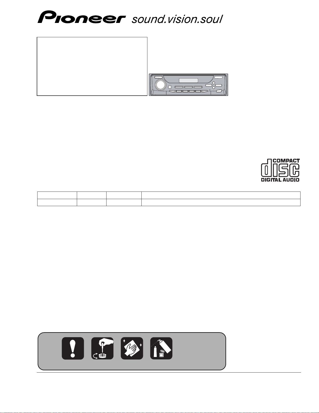
DEH-P840MP/XN/UC
MULTI-CD CONTROL HIGH POWER CD/MP3/WMA PLAYER WITH FM/AM TUNER
DEH-P840MP XN/UC
DEH-P8400MP XN/UC
DEH-P8450MP XN/ES
CONTENTS
1. SAFETY INFORMATION ............................................3
2. EXPLODED VIEWS AND PARTS LIST.......................4
3. BLOCK DIAGRAM AND SCHEMATIC DIAGRAM...18
4. PCB CONNECTION DIAGRAM ................................38
5. ELECTRICAL PARTS LIST ........................................48
6. ADJUSTMENT..........................................................55
7. GENERAL INFORMATION .......................................65
7.1 DIAGNOSIS ........................................................65
7.1.1 DISASSEMBLY .........................................65
7.1.2 CONNECTOR FUNCTION DESCRIPTION.......74
7.2 PARTS .................................................................75
7.2.1 IC................................................................75
7.2.2 DISPLAY....................................................92
7.3 OPERATIONAL FLOW CHART ...........................93
7.4 CLEANING ..........................................................93
8. OPERATIONS AND SPECIFICATIONS.....................94
2
DEH-P840MP,P8400MP,P8450MP
- CD Player Service Precautions
1. For pickup unit(CXX1550) handling, please refer
to"Disassembly"(see page 65)
During replacement, handling precautions shall be
taken to prevent an electrostatic discharge(protection
by a jumper-solder).
2. During disassembly, be sure to turn the power off
since an internal IC might be destroyed when a connector is plugged or unplugged.
3. Please checking the grating after changing the service pickup unit(see page 59).
[ Important symbols for good services ]
In this manual, the symbols shown-below indicate that adjustments, settings or cleaning should be made securely.
When you find the procedures bearing any of the symbols, be sure to fulfill them:
2. Adjustments
To keep the original performances of the product, optimum adjustments or specification confirmation is indispensable.
In accordance with the procedures or instructions described in this manual, adjustments should be performed.
3. Cleaning
For optical pickups, tape-deck heads, lenses and mirrors used in projection monitors, and other parts requiring cleaning,
proper cleaning should be performed to restore their performances.
5. Lubricants, glues, and replacement parts
Appropriately applying grease or glue can maintain the product performances. But improper lubrication or applying
glue may lead to failures or troubles in the product. By following the instructions in this manual, be sure to apply the
prescribed grease or glue to proper portions by the appropriate amount.For replacement parts or tools, the prescribed
ones should be used.
4. Shipping mode and shipping screws
To protect the product from damages or failures that may be caused during transit, the shipping mode should be set or
the shipping screws should be installed before shipping out in accordance with this manual, if necessary.
1. Product safety
You should conform to the regulations governing the product (safety, radio and noise, and other regulations), and
should keep the safety during servicing by following the safety instructions described in this manual.

3
DEH-P840MP,P8400MP,P8450MP
1. SAFETY INFORMATION
CAUTION
This service manual is intended for qualified service technicians; it is not meant for the casual do-it-yourselfer.
Qualified technicians have the necessary test equipment and tools, and have been trained to properly and safely repair
complex products such as those covered by this manual.
Improperly performed repairs can adversely affect the safety and reliability of the product and may void the warranty.
If you are not qualified to perform the repair of this product properly and safely, you should not risk trying to do so
and refer the repair to a qualified service technician.
W
ARNING
This product contains lead in solder and certain electrical parts contain chemicals which are known to the state of
California to cause cancer, birth defects or other reproductive harm.
Health & Safety Code Section 25249.6 - Proposition 65
4
DEH-P840MP,P8400MP,P8450MP
1
2
3
55
6
7
8
9
10
11
12
13
14
15
16
17
17
18
18
19
20
21
22
23
24
25
26
29
28
27
30
31
32
33
34
35
36
37
4
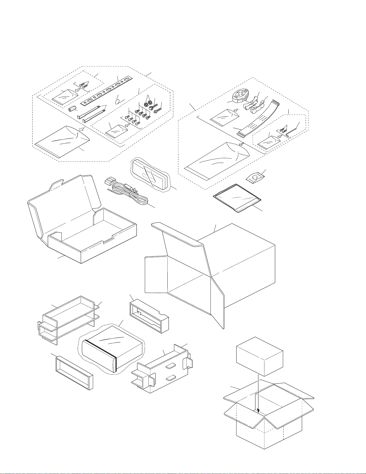
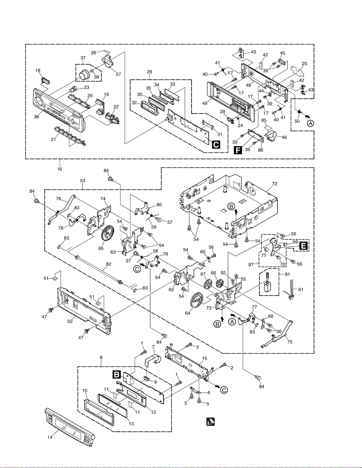
2. EXPLODED VIEWS AND PARTS LIST
2.1 PACKING (DEH-P840MP)

DEH-P840MP,P8400MP,P8450MP
5
1-1 Owner’s Manual CRD3569
1-2 Installation Manual CRD3570
* 1-3 Caution Card CRP1268
* 1-4 Warranty Card CRY1070
1-5 Polyethylene Bag CEG1116
2 Cord Assy CDE6563
3 Accessory Assy CEA3142
4 Spring CBH1650
5 Screw Assy CEA3140
6 Screw BPZ20P060FMC
* 7 Polyethylene Bag CEG-127
8 Handle CNC5395
9 Bush CNV3930
* 10 Polyethylene Bag CEG-158
11 Polyethylene Bag CEG1185
12 Case Assy CXB8574
* 13 Battery CEX1030
14 Sub Carton CHA3258
15 Carton CHG4661
16 Contain Box CHL4661
17 Protector CHP2538
18 Protector CHP2539
19 Protector CHP2541
20 Protector CHP2546
21 Remote Control Assy CXB9202
22 Screw Assy CZE3169
* 23 Polyethylene Bag CEG-127
* 24 Hexagonal Wrench CZE3176
* 25 Screw RMZ30H060FBK
26 Belt CZN7661
27 Holder Assy CZX3172
28 Holder Assy CZX3173
29 Remote Control Assy CZX3257
30 Screw Assy CEA3144
31 Screw BMZ50P060FMC
32 Screw CBA-102
33 Screw CBA1002
* 34 Polyethylene Bag CEG-127
35 Screw CMZ50P060FMC
36 Nut NF50FMC
37 Strap CNC5402
Mark No. Description Part No. Mark No. Description Part No.
- PACKING SECTION PARTS LIST (DEH-P840MP)
- Owner's Manual, Installation Manual
Part No. Language
CRD3569 English, French
CRD3570 English, French
NOTE:
- Parts marked by “*” are generally unavailable because they are not in our Master Spare Parts List.
- Screws adjacent to
∇ mark on the product are used for disassembly.
- For the applying amount of lubricants or glue, follow the instructions in this manual.
( In the case of no amount instructions, apply as you think it appropriate.)
6
DEH-P840MP,P8400MP,P8450MP
1
2
3
55
6
7
8
9
10
11
12
13
14
15
16
17
17
18
18
19
20
22
23
24
25
26
27
28
29
4
21
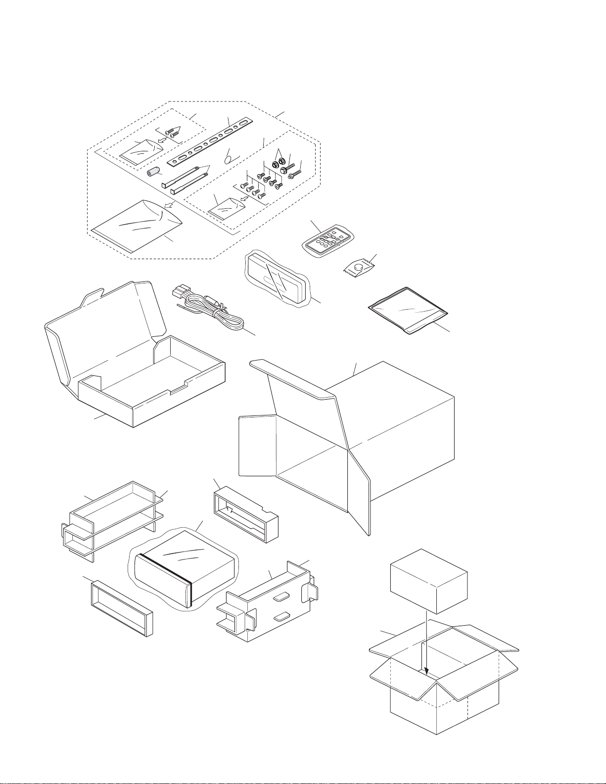
2.2 PACKING (DEH-P8400MP)

DEH-P840MP,P8400MP,P8450MP
7
1-1 Owner’s Manual CRD3571
1-2 Installation Manual CRD3572
* 1-3 Caution Card CRP1268
* 1-4 Card ARY1048
1-5 Polyethylene Bag CEG1116
2 Cord Assy CDE6563
3 Accessory Assy CEA3142
4 Spring CBH1650
5 Screw Assy CEA3140
6 Screw BPZ20P060FMC
* 7 Polyethylene Bag CEG-127
8 Handle CNC5395
9 Bush CNV3930
* 10 Polyethylene Bag CEG-158
11 Polyethylene Bag CEG1185
12 Case Assy CXB8574
* 13 Battery CEX1065
14 Sub Carton CHA3258
15 Carton CHG4662
16 Contain Box CHL4662
17 Protector CHP2538
18 Protector CHP2539
19 Protector CHP2541
20 Protector CHP2546
21 Remote Control Unit CXB8743
22 Screw Assy CEA3144
23 Screw BMZ50P060FMC
24 Screw CBA-102
25 Screw CBA1002
* 26 Polyethylene Bag CEG-127
27 Screw CMZ50P060FMC
28 Nut NF50FMC
29 Strap CNC5402
Mark No. Description Part No. Mark No. Description Part No.
- PACKING SECTION PARTS LIST (DEH-P8400MP)
- Owner's Manual, Installation Manual
Part No. Language
CRD3571 English, French
CRD3572 English, French
8
DEH-P840MP,P8400MP,P8450MP
1
2
3
8
9
10
11
12
13
14
15
16
17
17
18
18
19
20
21
22
23
24
25
26
29
28
27
30
31
33
34
35
4
2.3 PACKING (DEH-P8450MP)
DEH-P840MP,P8400MP,P8450MP
9
1-1 Owner’s Manual CRD3573
1-2 Owner’s Manual CRD3574
1-3 Installation Manual CRD3575
* 1-4 Caution Card CRP1268
1-5 Polyethylene Bag CEG1116
2 Cord Assy CDE6563
3 Accessory Assy CEA3143
4 Spring CBH1650
5-7 •••••
8 Handle CNC5395
9 Bush CNV3930
* 10 Polyethylene Bag CEG-158
11 Polyethylene Bag CEG1088
12 Case Assy CXB8574
* 13 Battery CEX1030
14 Sub Carton CHA3258
15 Carton CHG4663
16 Contain Box CHL4663
17 Protector CHP2538
18 Protector CHP2539
19 Protector CHP2541
20 Protector CHP2546
21 Remote Control Assy CXB9202
22 Screw Assy CZE3169
* 23 Polyethylene Bag CEG-127
* 24 Hexagonal Wrench CZE3176
* 25 Screw RMZ30H060FBK
26 Belt CZN7661
27 Holder Assy CZX3172
28 Holder Assy CZX3173
29 Remote Control Assy CZX3257
30 Screw Assy CEA2941
31 Screw BMZ50P060FMC
32 •••••
33 Screw CBA1002
* 34 Polyethylene Bag CEG-127
35 Screw CMZ50P060FMC
Mark No. Description Part No. Mark No. Description Part No.
- PACKING SECTION PARTS LIST (DEH-P8450MP)
- Owner's Manual, Installation Manual
Part No. Language
CRD3573 English, Spanish
CRD3574 Portuguese(B), Arabic
CRD3575 English, Spanish, Portuguese(B), Arabic
10
DEH-P840MP,P8400MP,P8450MP
2.4 EXTERIOR(1)
DEH-P840MP,P8400MP,P8450MP
11
1 Screw BMZ26P040FMC
2 Screw BSZ26P060FMC
3 Screw BSZ30P050FZK
4 Screw BSZ30P080FMC
5 Screw BSZ30P160FMC
6 Cord Assy CDE6563
7 Fuse(10A) CEK1136
8 •••••
9 Cap CNS1472
10 Resistor RS1/2PMF102J
11 Flat Cable CDE7021
12 Cord Assy CDE7026
13 Antenna Cable CDH1266
14 Holder CNC6469
15 Holder CNC8659
16 Holder CNC9708
17 Cushion CNM4870
18 Insulator CNM7543
19 Panel CNS6863
20 Tuner Amp Unit
See Contrast table(2)
21 Screw ASZ26P080FMC
22 Screw BMZ26P140FMC
23 Clamper CEF1008
24 Clamper CEF1009
25 Plug(CN981) CKM1278
26 Plug(CN811) CKS-787
27 •••••
* 28 Plug(CN101) CKS1058
29 Connector(CN832) CKS1082
* 30 Connector(CN831) CKS2211
31 Connector(CN351) CKS3606
32 Connector(CN723) CKS3835
33 Pin Jack(CN402) CKX1046
34 Holder CNC5399
35 Holder CNC9711
36 Holder CNC9713
37 Heat Sink CNR1615
38 FM/AM Tuner Unit CWE1563
39 Holder CNC8815
40 Case Unit CXB8524
41 Remote Control Assy
See Contrast table(2)
42 Cover See Contrast table(2)
43 CD Mechanism Module(S9MP3) CXK5556
44 IC(IC301) PAL007A
45 Screw ISS26P055FUC
46 Transistor(Q752,921) 2SD2396
47 Remote Control Unit
See Contrast table(2)
48 Cover See Contrast table(2)
Mark No. Description Part No. Mark No. Description Part No.
(1) EXTERIOR(1) SECTION PARTS LIST
Part No.
Mark No. Symbol and Description DEH-P840MP/XN/UC DEH-P8400MP/XN/UC DEH-P8450MP/XN/ES
20 Tuner Amp Unit CWM8042 CWM8043 CWM8044
41 Remote Control Assy CZX3257 Not used CZX3257
42 Cover CZN7655 Not used CZN7655
47 Remote Control Unit Not used CXB8743 Not used
48 Cover Not used CNS7068 Not used
(2) CONTRAST TABLE
DEH-P840MP/XN/UC, DEH-P8400MP/XN/UC and DEH-P8450MP/XN/ES are constructed the same except
for the following:
12
DEH-P840MP,P8400MP,P8450MP
2.5 EXTERIOR(2)
For lubricants points, please refer
to"Disassembly"(see page 65)

DEH-P840MP,P8400MP,P8450MP
13
1 Screw BPZ20P060FMC
2 Screw BPZ20P080FZK
3,4 •••••
5 Screw(M2x2) CBA1250
6 Holder CNC9800
7 Flexible PCB CNP6498
8 Keyboard Unit(OEL)
See Contrast table(2)
9 Connector(CN1801) CKS4175
10 Holder CNC9649
11 Tape CNM7514
12 Holder CNV6916
13 OEL Unit MXS8018
14 Sub Grille Assy
See Contrast table(2)
15 Case Unit CXB7967
16 Detach Grille Assy
See Contrast table(2)
17 Screw BPZ20P080FZK
18 Button(EJECT) CAC7241
19 Button(OPEN/BAND) CAC7242
20 Button(SRC/PAUSE/CLK) CAC7244
21 Button(1-6) CAC7246
22 Button(CROSS) CAC7247
23 Button(EQ) CAC7248
24 Spring CBH2543
25 Insulator CNM7649
26 Sheet CNM7824
27 Lighting Conductor CNV6913
28 Arm CNV6963
29 Keyboard Unit(LCD) CWM8056
30 LCD(LCD1901) CAW1704
31 Connector(CN1901) CKS4549
32 Holder CNC9648
33 Sheet CNM7512
34 Lighting Conductor CNV6914
35 Connector CNV6915
36 Grille Unit
See Contrast table(2)
37 Knob Assy CXB8026
38 Spring CBL1321
39 Screw(M2x2) CBA1250
40 Screw CBA1561
41 Spring CBH2530
42 Cushion CNM7551
43 Arm CNV6962
44 Guide CNV6967
45 Guide CNV6968
46 Flexible PCB CNP6869
47 Screw ISS26P055FUC
48 Case Unit CXB7968
49 Cover Unit CXB8127
50 Spring CBH2545
51 Cushion CNM7550
52 Panel Unit CXB7953
53 Drive Unit CXB8138
54 Screw BMZ26P040FMC
55 Screw(M2x3) CBA1061
56 Screw(M2x2) CBA1250
57 Screw(M2x1.4) CBA1562
58 Spring CBH2525
59 Spring CBH2526
60 Spring CBL1557
61 Cord CDE6737
62 Holder CNC9678
63 Holder CNC9679
64 Gear CNV6932
65 Gear CNV6933
66 Gear CNV6935
67 Gear CNV6936
68 Lever CNV6937
69 Switch(S951) CSN1051
70 Spring Switch(S952) CSN1052
71 Switch(S953) CSN1058
72 Chassis Unit CXB7956
73 Holder Unit CXB7959
74 Holder Unit CXB7960
75 Arm Unit CXB7961
76 Arm Unit CXB7962
77 Arm Unit CXB7963
78 Arm Unit CXB7964
79 Arm Unit CXB7965
80 Arm Unit CXB7966
81 Motor Unit(M951) CXB8939
82 Gear Unit CXB8940
83 Washer YE15FUC
84 Screw CBA1559
85 Sheet CNM7839
86 PCB CNX3607
87 Switch Unit CWS1370
Mark No. Description Part No. Mark No. Description Part No.
(1) EXTERIOR(2) SECTION PARTS LIST

14
DEH-P840MP,P8400MP,P8450MP
Part No.
Mark No. Symbol and Description DEH-P840MP/XN/UC DEH-P8400MP/XN/UC DEH-P8450MP/XN/ES
8 Keyboard Unit(OEL) CWM8051 CWM8052 CWM8052
14 Sub Grille Assy CXB9363 CXB9362 CXB9364
16 Detach Grille Assy CXB8092 CXB8093 CXB8094
36 Grille Unit CXB7942 CXB7941 CXB7943
(2) CONTRAST TABLE
DEH-P840MP/XN/UC, DEH-P8400MP/XN/UC and DEH-P8450MP/XN/ES are constructed the same except
for the following:

DEH-P840MP,P8400MP,P8450MP
15
16
DEH-P840MP,P8400MP,P8450MP
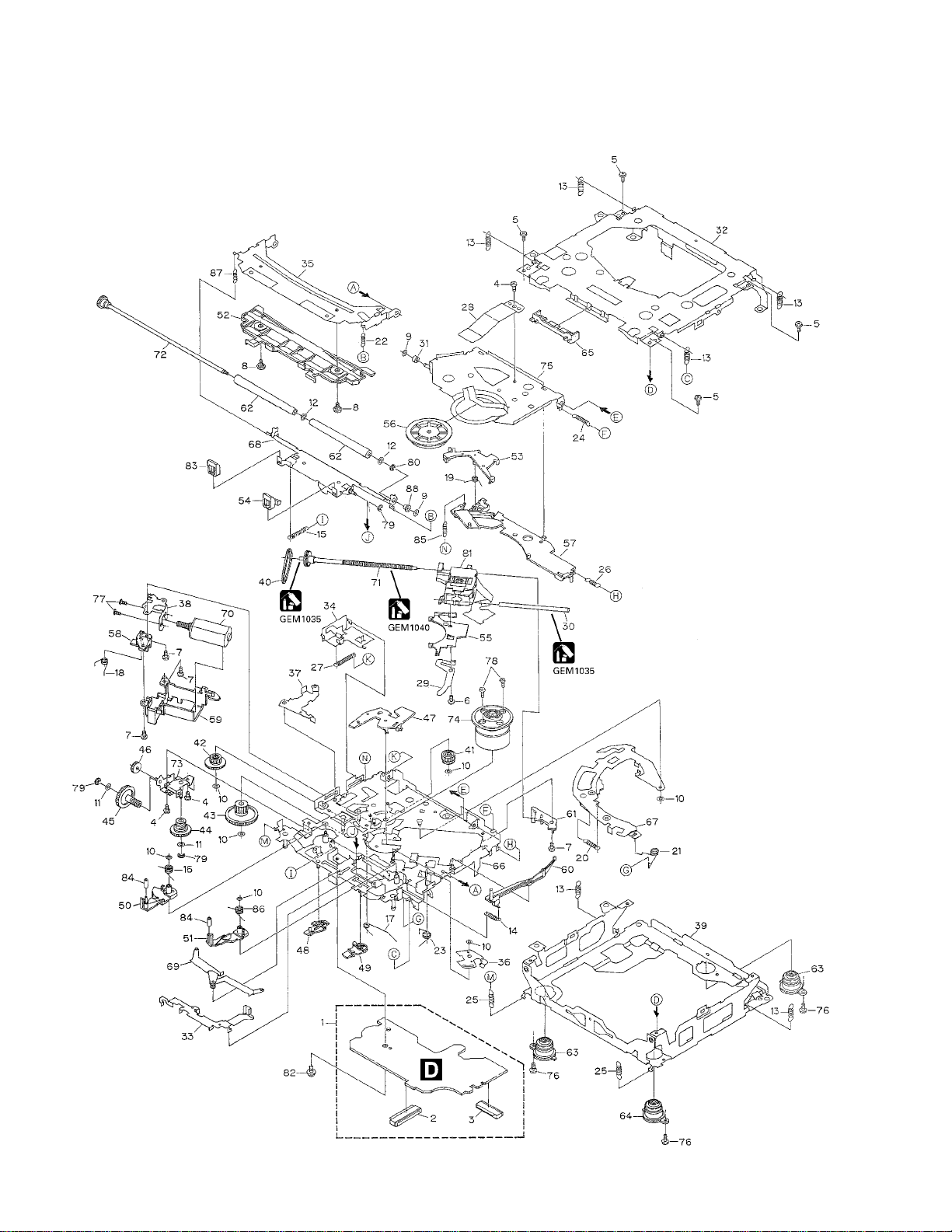
2.6 CD MECHANISM MODULE

DEH-P840MP,P8400MP,P8450MP
17
Mark No. Description Part No. Mark No. Description Part No.
1 CD Core Unit(S9MP3) CWX2618
2 Connector(CN901) CKS4188
3 Connector(CN101) CKS3486
4 Screw BMZ20P025FMC
5 Screw BSZ20P040FMC
6 Screw(M2x4) CBA1362
7 Screw(M2x3) CBA1527
8 Screw CBA1545
9 Washer CBF1037
10 Washer CBF1038
11 Washer CBF1039
12 Washer CBF1060
13 Spring CBH2378
14 Spring CBH2379
15 Spring CBH2514
16 Spring CBH2533
17 Spring CBH2382
18 Spring CBH2383
19 Spring CBH2384
20 Spring CBH2527
21 Spring CBH2386
22 Spring CBH2537
23 Spring CBH2390
24 Spring CBH2391
25 Spring CBH2523
26 Spring CBH2426
27 Spring CBH2444
28 Spring CBL1561
29 Spring CBL1553
30 Shaft CLA3845
31 Roller CLA3910
32 Frame CNC9654
33 Lever CNC9664
34 Lever CNC8949
35 Arm CNC9661
36 Arm CNC9016
37 Arm CNC9017
38 Bracket CNC9123
39 Frame CNC9656
40 Belt CNT1086
41 Gear CNV6886
42 Gear CNV6316
43 Gear CNV6317
44 Gear CNV6318
45 Gear CNV6319
46 Gear CNV6320
47 Arm CNV6322
48 Arm CNV6323
49 Arm CNV6324
50 Arm CNV6888
51 Arm CNV6889
52 Guide CNV6327
53 Arm CNV6924
54 Guide CNV6921
55 Rack CNV6923
56 Clamper CNV6331
57 Arm CNV6332
58 Guide CNV6333
59 Cover CNV6334
60 Arm CNV6335
61 Guide CNV6336
62 Roller CNV6338
63 Damper CNV6175
64 Damper CNV6662
65 Guide CNV6925
66 Chassis Unit CXB7980
* 67 Arm Unit CXB7983
68 Arm Unit CXB7984
69 Arm Unit CXB7985
70 Motor Unit(M2) CXB5903
71 Screw Unit CXB5904
72 Gear Unit CXB8076
73 Bracket Unit CXB7982
74 Motor Unit(M1) CXB6007
75 Arm Unit CXB8504
76 Screw(M2x5) EBA1028
77 Screw JFZ20P020FMC
78 Screw JGZ17P020FZK
79 Washer YE15FUC
80 Washer YE20FUC
81
Pickup Unit(Service)(P9MP3) CXX1550
82 Screw IMS26P030FMC
83 Guide CNV6922
84 Roller CNV6887
85 Spring CBH2509
86 Spring CBH2512
87 Spring CBH2536
88 Collar CNV6906
- CD MECHANISM MODULE SECTION PARTS LIST
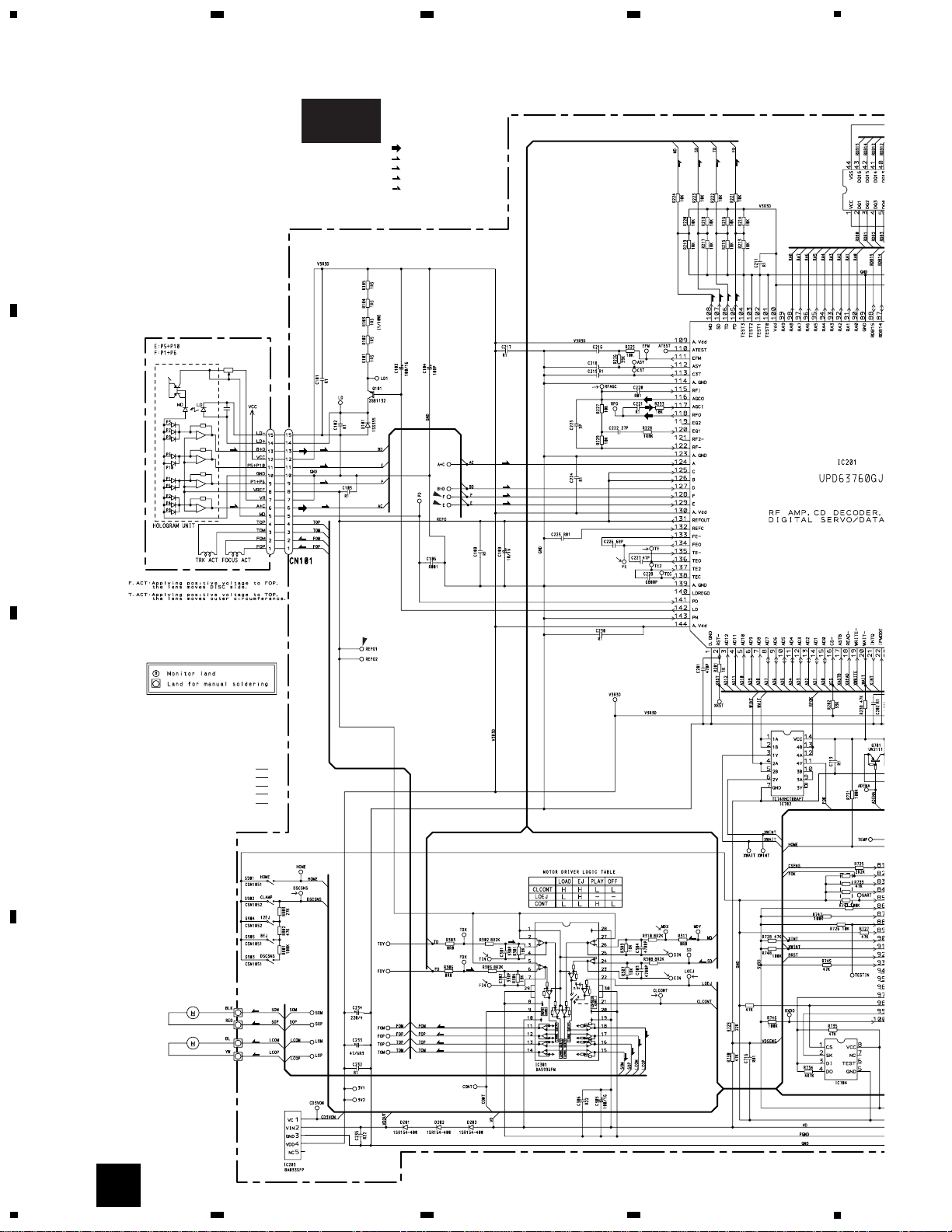
IC 102
HA12187FP
IP-BUS DRIVER
PEE
24
SYSTEM CONTR
IC 601(2/2)
CN402
VDD
VCC
ANT
1
2
BUS-
BU
BUS+
BUSL+
BUSL-
1
2
8
6
5
TX
RX
IPPW
CN723
TUNER AMP UNIT
14
ASENB1
TUN L
BUSL+
BUSL-
CD L
Q101
Q102
P-BUS
P-BUS
VDD
Q602
Q603
MUTE
5
8
1
7
CN101
11
BUZZER
IC 3
EEPROM
FM/AM TUNER UNIT
28
27
FM/AM 1ST IF 10.7MHz
T51 Q51 CF51
CF52 CF53
IC1
MIXER, IF AMP, DET.
6
21
18
LDET
COMP
222510 14 12 15 16 8 13 2 3 4
CF202
VDD
VCC
DI/DO
CE2CKCE1
SDBWSLFMSD
NL1
NL2
IC 2 FM MPX
AMANT
FMANT
ATT
ATT
AMRF
FMRF
RF ADJ
ANT2 ADJ
X901
10.25MHz
ANT1 ADJ
LOCL
23
LOCH
AMDET
MPXREF 41kHz
AM 2ND IF
450kHz
19
CREQ
11
DGND
1
STIND
L ch
5
R ch
924
NC
FMLOCL
20177
NCNCWC
26
RFGND
CN901
Q101
M
LASER
DIODE
MONITOR
DIODE
CLAMP
SENSE
DISC
SENSE
FOCUS ACT.
SPINDLE
MOTOR
M
CARRIAGE
MOTOR
LOAD/
TRACKING ACT.
LD-
MD
FO+
TO+
15
5
1
4
PICKUP UNIT
(SERVICE)(P9MP3)
HOLOGRAM
UNIT
IC 301
BA5996FM
IC 201
UPD63760GJ
IC 703
+3.3V REGULATOR
RF-AMP,CD DECODER,
MP3 DECODER,
DIGITAL SERVO / DATA PROCESSOR
CD
DRIVER
2
VD
VD
3VDD
14
L-OUT
1
CN101
TOP
FOP
16
SOP
15
SOM
18
LCOP
17
LCOM
22
4,5
LOEJ
43
35
LOUT
42
9
CONT
12
FOP
TD/FD
AC,BD
F,E
SD/MD
1
13
TOP
S901
HOME
12EJ
SENSE
8EJ
SENSE
LD+
14
142
LD
141
PD
20
8
21
CD CORE UNIT(S9MP3)
3938
X201 X202
DSCSNS
CONT
LOEJ
HOME
78
80
31
29
5VDD
IC 203
BA033SFP
+3.3V REGULATOR
V3R3D
2
4
VD
CD3VON
28
VDCONT
27
1
S-818A33AUC-BGN
CD CONTROLLER
IC 701
PE5269A
33
CDMUTE
3
19
V3R3D
WAIT,
RFOK
IC 501
UPD61002GC
DRAM
IC 202
MSM51V4265EP-70TS
WMA DECODER
TC74VHCT08AFT
IC 702
XWINT,
XWAIT,
FOK
Q751
7
VDCONT
Q752
BU
15
IC 251
BA3834F
SPECTRUM ANALYZER
VR231
MIC231
6
4
1
2
3
5
CN811
VD
FEJSW1
FOPSW1
FCLSW1
MOTOR2
MOTOR1
IC 811
BA6288FS
3
14
Q812
Q811
BU
FLPPW
11
45
6
11
66
65
FLPOPN
FLPCLS
69
68
67
fclssw
fopnsw
flpejsw
M
AUTOMATIC
FLAP MOTOR
CLOSE
OPEN
EJECT
SWITCH PCB
IC 502
BA25BC0WFP
2
4
V2R5
1
+2.5V REGULATOR
A
E
D
PD5740A(E
PD5741A(U
18
DEH-P840MP,P8400MP,P8450MP
A
1
234
B
C
D
12
34
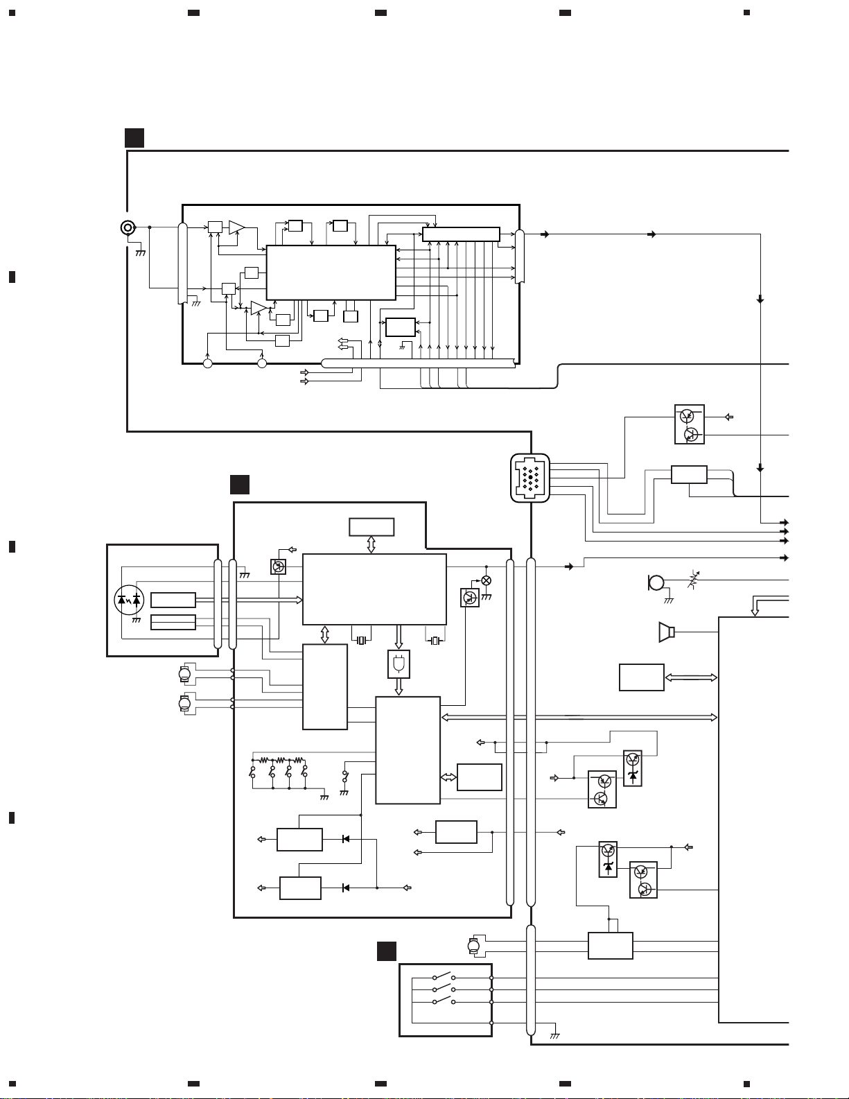
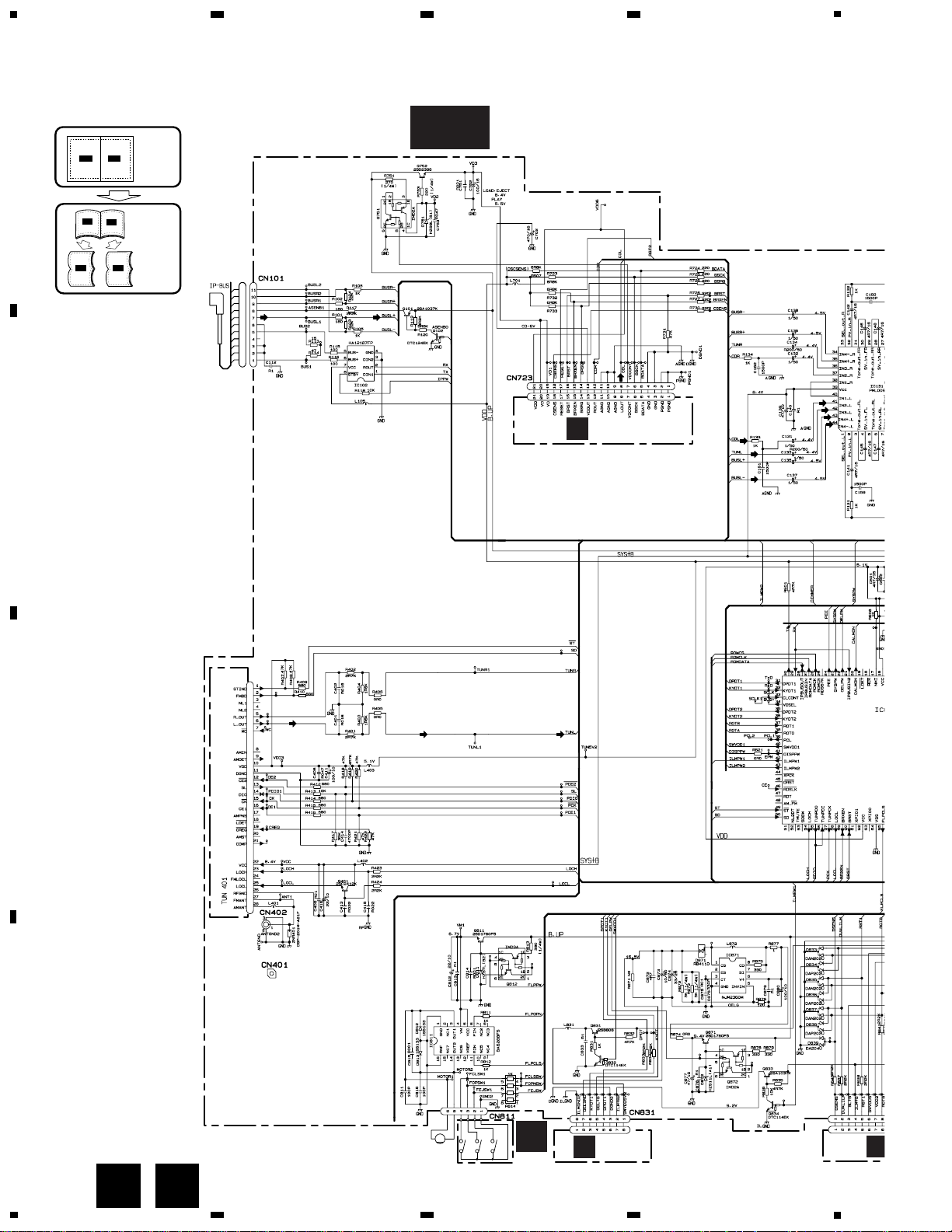
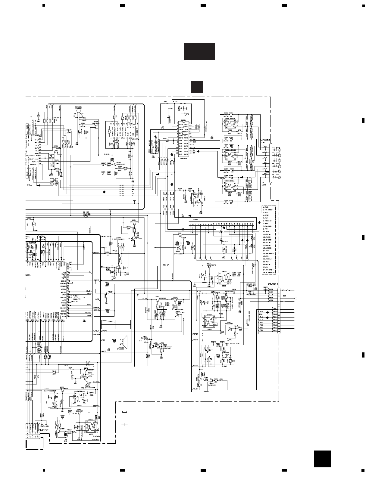
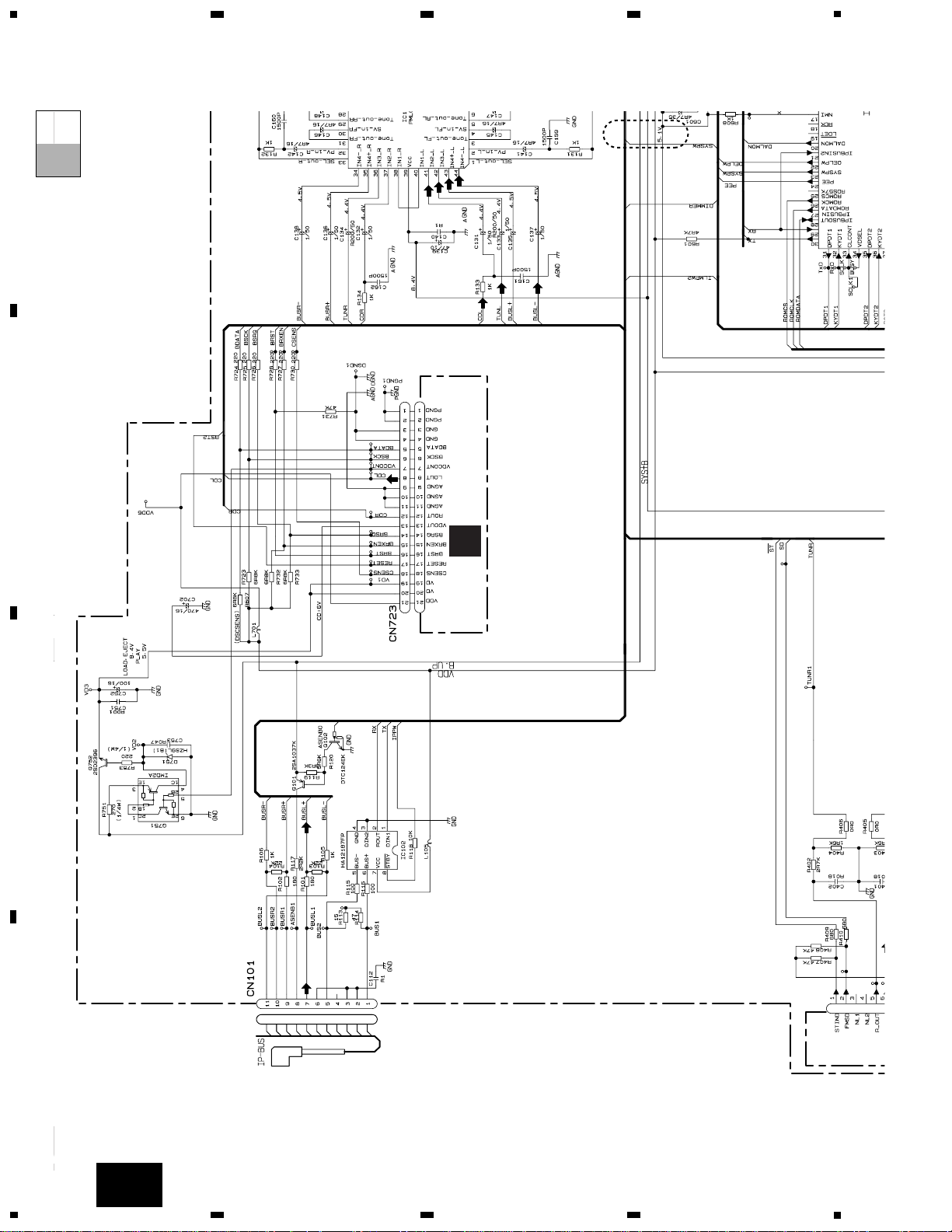
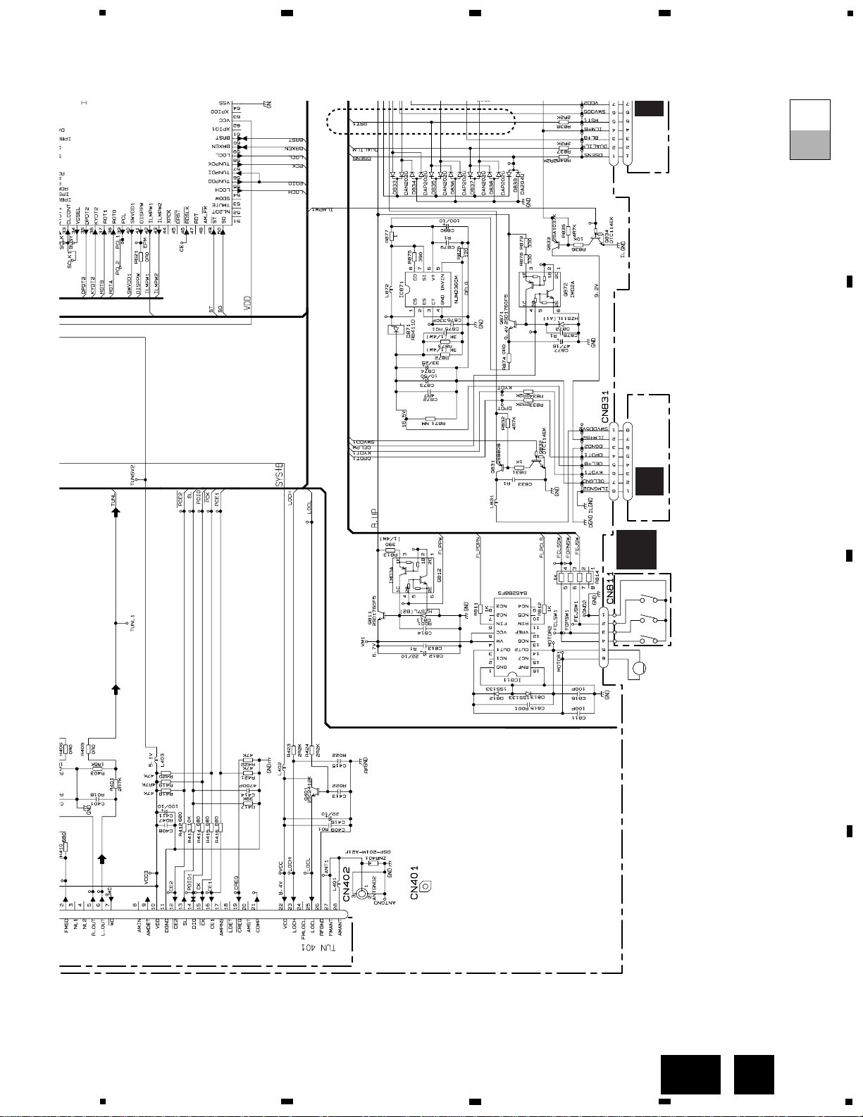
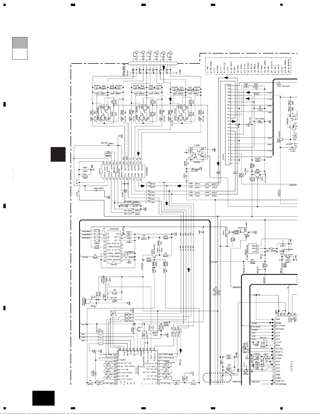
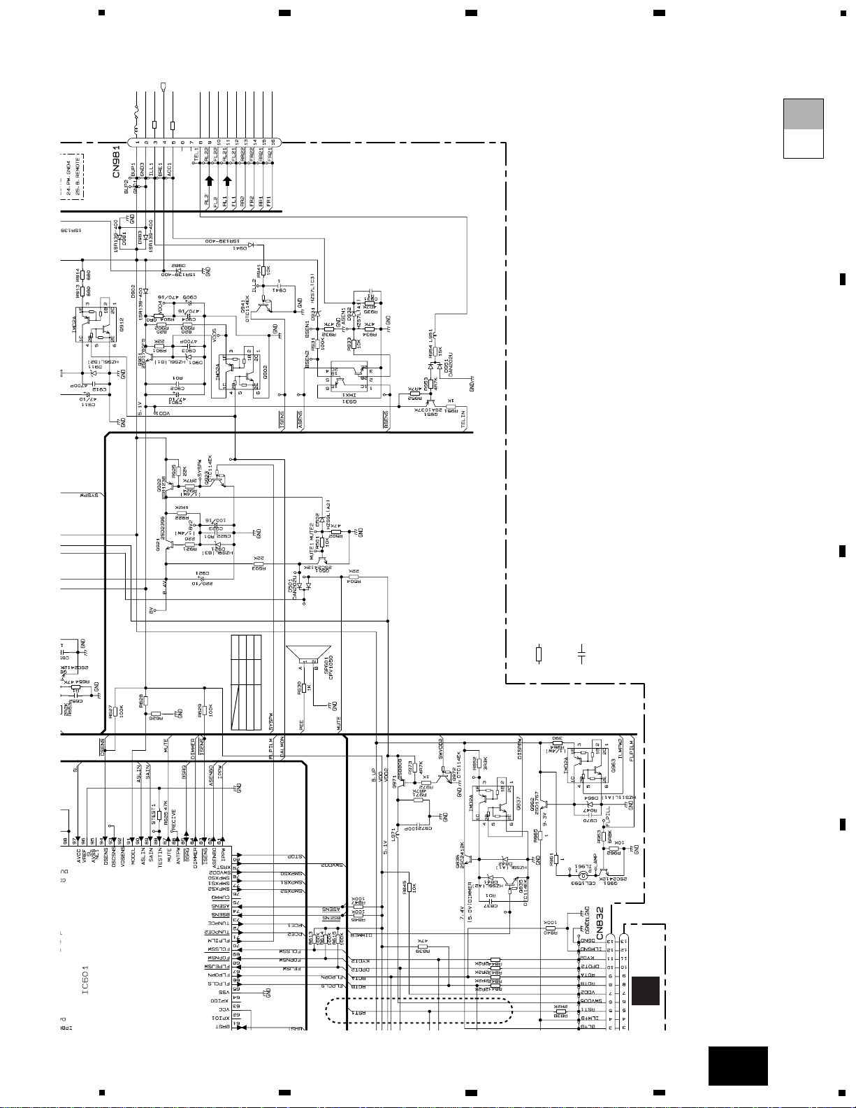
3. BLOCK DIAGRAM AND SCHEMATIC DIAGRAM
3.1 BLOCK DIAGRAM
12
1
VDD
BU
74
73
SD
SL
TUNPCE
TUNPCK
TUNPDO
ASENBO
10
FL
11
RL
87
MUTE
XOUT
XIN
3
5
23
21
FLFL+
RLRL+
50
97
IN3-L
42
IN4+L
43
IN4-L
44
IN2-L
41
72
57
71
55
82
30 29 81
FLIN
12
RLIN
14
22 4
RESET
POWER AMP
IC 601(1/2)
IC 601(2/2)
IC 131
PML009A
IC 651
S-80735ANDZI
IC 301
PAL007A
RESET
VDD
Q901
Q931
SYSPW
TXRXIPPW
ELECTRONIC VOLUME/
SOURCE SELECTOR
STBYMUTE
13
X601
15
2
ACC
VST,VCK,VDT
TUN L
SYS+B
BU
Q922
Q923
23
SYSPW
Q301
FL
Q351
FL
Q352
RL
Q353
RL
SW
12
PL
MUTE
SYSTEM CONTROLLER
Q941
Q951
VDD
83
TELIN
10
25
B.REMOTE
IN1-L
VDD REGULATOR
ILL SENSE
BACKUP SENSE
ACC SENSE
TELEPHONE MUTE
SYS+B REGULATOR
5
9
11
12
10
1
3
8
4
2
IC 571
PA2028A
HIGH OUT
OUT1
18
OUT3
16
OUT5
14
11
7
9
IN5
IN1
IN3
PL
FL
RL
CN981
Q503
BU
CN351
BACK UP
GND
ACC
ILL
TELMUTE
B.REM
FL-
FL+
RLRL+
Q921
Q501
MUTE
11
7
3
SW
bsens
asens
isens
PD5740A(ES)
PD5741A(UC)
tunpce@
13
MIC_IN
Q872
Q871
BU
OELPW
22
IC 871
NJM2360M
6
1
5
CN831
4
6
OEL+B
DPDT1
KYDT1
DPDT1
31
KYDT1
32
Q831
Q832
VDD2
SWVDD1
40
1
SWVDD5V
Q963
Q962
BU
ILMPW2
43
4
CN832
10
11
ILM+B
DPDT2
KYDT2
DPDT2
35
KYDT2
36
Q971
Q972
VDD2
SWVDD2
79
6
SWVDD5
Q833
Q834
ILMPW1
42
2
ILM+B2
OEL+B REGULATOR
ILM+B REGULATOR
4
10
11
6
4
5
3
8
7
CN1801
OEL+B
DPDT2
KYDT2
SWVDD5V2
ILM+B2
CN1901
ILM+B
DPDT
KYDT
SWVDD5V
KEYBOARD UNIT(LCD)
KEYBOARD UNIT(OEL)
Q651
5
RST1
5
RST
VDD2
Q911
ACC
5V REGULATOR
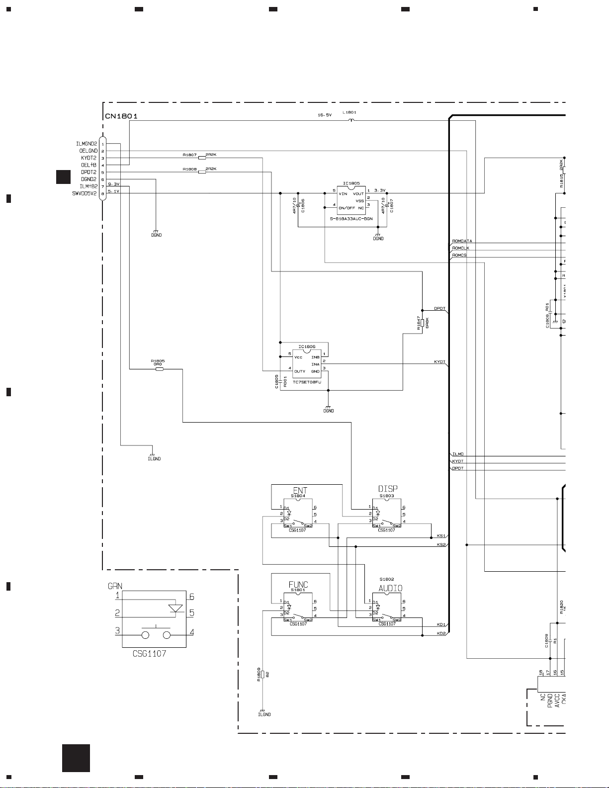
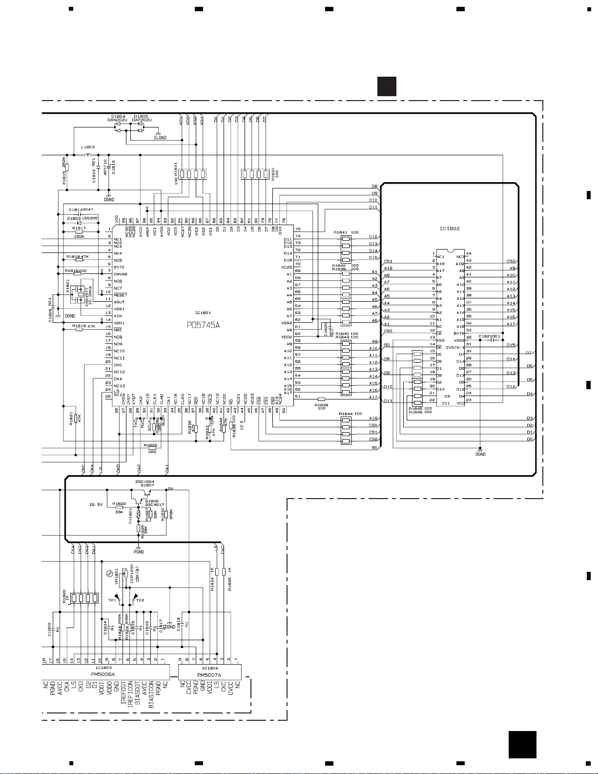
IC 1801
PD5745A
GRILLE µ-COM
KEY MATRIX
IC 1802
PD8091A
(DEH-P840MP)
PD8092A
(DEH-P8400MP,P8450MP)
ROM
OEL UNIT
Q1807
Q1806
4
IC 1806
TC7SET08FU
228
27
DPDT
KYDT
5
IC 1805
S-818A33AUC-BGN
1
3.3V
8
XOUT
XIN
11
X1801
13
IC 1902
PD6340A
GRILLE µ-COM
KEY MATRIX
LCD
20
18
DPDT
KYDT
XO
XI
22
X1901
23
SW5V
4
IC 1901
RS-140
1
17
REM
OPT IN
SW5V
VDD
77
RESET
B
C
CONNECTOR PCB
F
PD5740A(ES)
PD5741A(UC)
10A
FUSE
B.UP
ACC
ILM
MUTE
GND
FLFL+
RLRL+
B.REM
DEH-P840MP,P8400MP,P8450MP
5
6
7
8
A
B
C
D
5
6
7
8
19
A
E
A-a A-b
A-a
A-b
A-b
A-a
Large size
SCH diagram
Guide page
Detailed page
Note: When ordering service parts, be sure to refer to " EXPLODED VIEWS AND PARTS LIST" or
"ELECTRICAL PARTS LIST".
A-a
The > mark
the importanc
Therefore, wh
identical desi
D
CN901
B
CN1801
F
FM/AM TUNER UNIT
M
SWITCH PCB
E
M951
AUTOMATIC FLAP
CXB8939
CSN1052
(CLOSE)
CSN1051
(OPEN)
CSN1058
(EJECT)
IP-BUS
DRIVER
VD REG
E-VOL
OEL+B REG
SW VDD
FLAP MOTOR
AND SENSE
SYSTEM C
FM(100%):-19.5dBs
AM(30%):-30.0dBs
FM:-20.5dBs
AM:-31.0dBs
IP-BUS:+2.2dBs
CD:0.0dBs
TUNER
PD5
(DEH-P840M
PD5
(DEH-P8
20
DEH-P840MP,P8400MP,P8450MP
A
1
234
B
C
D
12
34
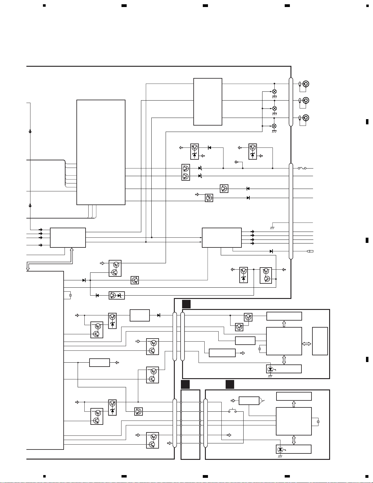
3.2 OVERALL CONNECTION DIAGRAM(GUIDE PAGE)
A
E
A-b
**
**
GND
RL—
RL+
FL—
FL+
B.REM
ILL
ACC
TEL
CEK1136
10A
RR—
RR+
FR—
FR+
>
FRONT
L CH
SUB
WOOFER
L CH
RCA OUT
SUB
WOOFER
R CH
FRONT
R CH
REAR
L CH
REAR
R CH
Decimal points for resistor
and capacitor fixed values
are expressed as :
2.2 2R2
0.022 R022
←
←
Symbol indicates a resistor.
No differentiation is made between chip resistors and
discrete resistors.
NOTE :
Symbol indicates a capacitor.
No differentiation is made between chip capacitors and
discrete capacitors.
found on some component parts indicates
ce of the safety factor of the part.
A
TUNER AMP UNIT
ASL
SPECTRUM
ANALYSER
HI-OUT
MUTE
POWER AMP
RESET
5V REG
VDD REG
SENSE
TEL MUTE
SYS+B REG
MUTE
SW
VDD
BL+B
REG
ILM+B
REG
FM:+2.6dBs
AM:-7.9dBs
IP-BUS:+8.3dBs
CD:+8.1dBs
FM:+10.1dBs
AM:-0.4dBs
IP-BUS:+15.8dBs
CD:+15.6dBs
FM:+28.6dBs
AM:+18.1dBs
IP-BUS:+34.3dBs
CD:+34.1dBs
8450MP)
DEH-P840MP
DEH-P8400MP
DEH-P8450MP
R626 R628
100K
100K
100K
Not used
**
12
11
10
9
8
7
6
5
4
3
2
1
PAL007A
Not used
Not used
21
DEH-P840MP,P8400MP,P8450MP
5
6
7
8
A
B
C
D
5
6
7
8
A
1
The > mar
the importa
Therefore, w
identical de
D
CN901
IP-BUS
DRIVER
VD REG
E-V
SYSTEM
M(100%):-19.5dBs
AM(30%):-30.0dBs
FM:-20.5dBs
AM:-31.0dBs
IP-BUS:+2.2dBs
CD:0.0dBs
TUNER
22
DEH-P840MP,P8400MP,P8450MP
A
1
234
B
C
D
12
34
A-a
A-b
A-a
A-a
A-b
A-a
A-a
A-b
E
2
B
CN1801
F
FM/AM TUNER UNIT
M
SWITCH PCB
E
M951
AUTOMATIC FLAP
CXB8939
CSN1052
(CLOSE)
CSN1051
(OPEN)
CSN1058
(EJECT)
OEL+B REG
SW VDD
FLAP MOTOR
AND SENSE
SYSTEM
FM(100%):-19
AM(30%):-30
PD
(DEH-P84
PD
(DEH
23
DEH-P840MP,P8400MP,P8450MP
5
6
7
8
A
B
C
D
5
6
7
8
A-a
A-b
A-a
E
A-a
A-b
1
FRONT
L CH
SUB
WOOFER
L CH
RCA OUT
SUB
WOOFER
R CH
FRONT
R CH
REAR
L CH
REAR
R CH
A
TUNER AMP UNIT
E-VOL
ASL
SPECTRUM
ANALYSER
HI-OUT
MUTE
POWER AMP
RESET
5V REG
FM:+2.6dBs
AM:-7.9dBs
IP-BUS:+8.3dBs
CD:+8.1dBs
FM:+10.1dBs
AM:-0.4dBs
IP-BUS:+15.8dBs
CD:+15.6dBs
121110
987654321
PAL007A
24
DEH-P840MP,P8400MP,P8450MP
A
1
234
B
C
D
12
34
A-a
A-b
A-b
A-a
A-b
A-b
2
**
**
GND
RL—
RL+
FL—
FL+
B.REM
ILL
ACC
TEL
CEK1136
10A
RR—
RR+
FR—
FR+
>
Decimal points for resistor
and capacitor fixed values
are expressed as :
2.2 2R2
0.022 R022
←
←
Symbol indicates a resistor.
No differentiation is made between chip resistors and
discrete resistors.
NOTE :
Symbol indicates a capacitor.
No differentiation is made between chip capacitors and
discrete capacitors.
F
5V REG
VDD REG
SENSE
TEL MUTE
SYS+B REG
MUTE
SW
VDD
BL+B
REG
ILM+B
REG
FM:+28.6dBs
AM:+18.1dBs
IP-BUS:+34.3dBs
CD:+34.1dBs
PD5741A
(DEH-P840MP, P8400MP)
PD5740A
(DEH-P8450MP)
DEH-P840MP
DEH-P8400MP
DEH-P8450MP
R626 R628
100K
100K
100K
Not used
**
Not used
Not used
25
DEH-P840MP,P8400MP,P8450MP
5
6
7
8
A
B
C
D
5
6
7
8
A-b
A-a
A-b
26
DEH-P840MP,P8400MP,P8450MP
A
1
234
B
C
D
12
34
B
A
CN831
B
3.3 KEYBOARD UNIT(OEL)
DEH-P840MP,P8400MP,P8450MP
5
6
7
8
A
B
C
D
5
6
7
8
27
B
B
KEYBOARD UNIT(OEL)
OEL UNIT
MXS8018
ROM
GRILLE µ-COM
PD8091A(DEH-P840MP)
PD8092A(DEH-P8400MP, P8450MP)
B
C
A
CN832
RESET
VOLUME
CLK PAUSE
SRC
REMOTE CONTROL
SENSOR
F
CONNECTOR
PCB
28
DEH-P840MP,P8400MP,P8450MP
A
1
234
B
C
D
12
34
C
F
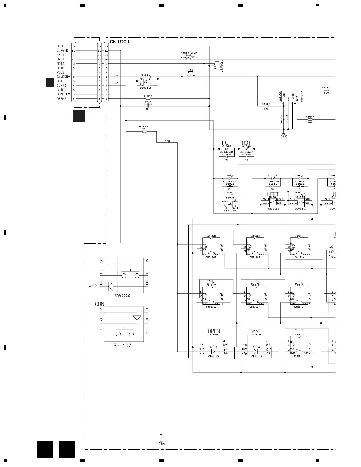
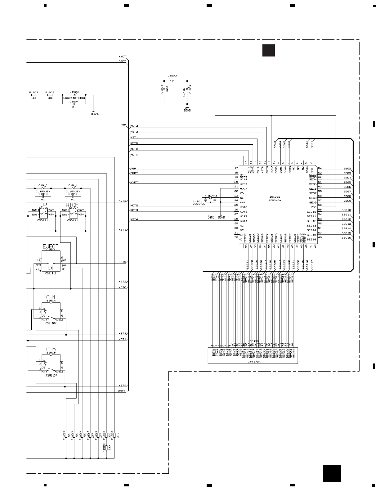
3.4 KEYBOARD UNIT(LCD)
C
C
KEYBOARD UNIT(LCD)
LCD
GRILLE µ-COM
29
DEH-P840MP,P8400MP,P8450MP
5
6
7
8
A
B
C
D
5
6
7
8
C
D
D-a
R750
PD9023A
3300P
R022
SPINDLE MOTOR
M1 CXB6007
LOADING/CARRIAGE
MOTOR
M2 CXB5903
SWITCHES:
CD CORE UNIT(S9MP3)
S901 : HOME SWITCH ON-OFF
S902 : CLAMP SWITCH ON-OFF
S903 : DSCSNS SWITCH ON-OFF
S904 : 12EJ SWITCH ON-OFF
S905 : 8EJ SWITCH ON-OFF
....
........
......
...........
............
The underlined indicates the switch
position.
PICKUP UNIT
(SERVICE)(P9MP3)
F
T
C
S
SIGNAL LINE
FOCUS SERVO LINE
TRACKING SERVO LINE
CARRIAGE SERVO LINE
SPINDLE SERVO LINE
F
F
F
F
F
F
F
F
F
F
F
F
T
T
T
T
T
C
S
T
T
T
S
C
S
S
C
C
S
S
C
C
1
2
3
5
6
7
8
0
!
@
#
F
T
C
S
30
DEH-P840MP,P8400MP,P8450MP
A
1
234
B
C
D
12
34
3.5 CD MECHANISM MODULE(GUIDE PAGE)
D

D-b
D
D
CD CORE UNIT (S9MP3)
A
CN723
4
9
$
%
16
*
&
31
DEH-P840MP,P8400MP,P8450MP
5
6
7
8
A
B
C
D
5
6
7
8
D

32
DEH-P840MP,P8400MP,P8450MP
A
1
234
B
C
D
12
34
Aa
Db
Da
1
3300P
R022
PICKUP UNIT
(SERVICE)(P9MP3)
F
T
C
S
SIGNAL LINE
FOCUS SERVO LINE
TRACKING SERVO LINE
CARRIAGE SERVO LINE
SPINDLE SERVO LINE
F
F
F
F
F
F
F
F
F
T
T
T
T
T
C
S
0
!
#
F
T
C
S
D-a
D-a
D-b

33
DEH-P840MP,P8400MP,P8450MP
5
6
7
8
A
B
C
D
5
6
7
8
D-
D-
2
3
4
5
6
R750
PD9023A
SPINDLE MOTOR
M1 CXB6007
LOADING/CARRIAGE
MOTOR
M2 CXB5903
SWITCHES:
CD CORE UNIT(S9MP3)
S901 : HOME SWITCH ON-OFF
S902 : CLAMP SWITCH ON-OFF
S903 : DSCSNS SWITCH ON-OFF
S904 : 12EJ SWITCH ON-OFF
S905 : 8EJ SWITCH ON-OFF
....
........
......
...........
............
The underlined indicates the switch
position.
F
F
F
T
T
T
S
C
S
S
C
C
S
S
C
C
1
2
3
5
6
7
8
@
D-a
D-a
D-b

34
DEH-P840MP,P8400MP,P8450MP
A
1
234
B
C
D
12
34
D-a
D-b
1
D
CD CORE UNIT (S9MP3)
9
$
%
16
D-b
D-a
D-b

35
DEH-P840MP,P8400MP,P8450MP
5
6
7
8
A
B
C
D
5
6
7
8
D-a
D-b
D-b
2
3
4
5
6
A
CN723
4
*
&
D-b
D-a
D-b

36
DEH-P840MP,P8400MP,P8450MP
! CH1:FE 500mV/div.
8 CH2:FIN 500mV/div.
0 CH3:TE 500mV/div.
7 CH4:TIN 500mV/div.
During "Play" (CD-DA)
- Waveforms
1 CH1:DSCSNS 5V/div.
2 CH2:CLCONT 5V/div.
3 CH3:LOEJ 5V/div.
4 CH4:VD 10V/div.
When loading an 8cm CD
500ms/div.
5 CH1:SIN 1V/div.
6 CH2:CIN 500mV/div.
7 CH3:TIN 500mV/div.
When setting up after loading a
12cm CD-DA disc
2s/div.
5 CH1:SIN 1V/div.
6 CH2:CIN 500mV/div.
7 CH3:TIN 500mV/div.
When setting up after loading a
12cm CD-ROM(2 session)
2s/div.
5 CH1:SIN 1V/div.
6 CH2:CIN 500mV/div.
7 CH3:TIN 500mV/div.
When setting up after loading a
12cm CD-ROM(1 session)
2s/div.
1 CH1:DSCSNS 5V/div.
2 CH2:CLCONT 5V/div.
3 CH3:LOEJ 5V/div.
4 CH4:VD 10V/div.
When loading a 12cm CD
Ref. :
GND
Mode :
Normal
Ref. :
GND
Mode :
Normal
Ref. :
REFO
Mode :
Normal
Ref. :
REFO
Mode :
Normal
Ref. :
REFO
Mode :
Normal
Ref. :
REFO
Mode :
Normal
Ref. :
REFO
Mode :
Normal
Ref. :
REFO
Mode :
Normal
Ref. :
REFO
Mode :
Normal
Ref. :
REFO
Mode :
Normal
Ref. :
REFO
Mode :
Normal
Ref. :
REFO
Mode :
Normal
500ms/div.
8 CH1:FIN 200mV/div.
9 CH2:RFOK 2V/div.
5 CH3:SIN 2V/div.
When setting up "Source On"
(12cm CD-DA)
500ms/div.
20ms/div.
! CH1:FE 500mV/div.
8 CH2:FIN 500mV/div.
0 CH3:TE 500mV/div.
7 CH4:TIN 500mV/div.
During "Play"(CD-ROM, generating 1Track
Jump periodically) Refer to "1Track Jump."
20ms/div.
@ CH1:MDX 500mV/div.
5 CH2:SIN 1V/div.
Spindle waveform during "Play"
5ms/div.
@ CH1:MDX 500mV/div.
5 CH2:SIN 1V/div.
Spindle waveform during "Play"
(Magnified)
5µs/div.
# CH1:RFAGC 500mV/div.
RF eye pattern
5µs/div.
0 CH1:TE 500mV/div.
! CH2:FE 500mV/div.
When setting up "Source On"
200ms/div.
Note:1. The encircled numbers denote measuring points in the circuit diagram.
2. Reference voltage
REFO1 : 1.65V

37
DEH-P840MP,P8400MP,P8450MP
# CH1:RFAGC 1V/div.
7 CH2:TIN 1V/div.
0 CH3:TE 1V/div.
8 CH4:FIN 1V/div.
When reproducing black dots(800µm)
500µs/div.
0 CH1:TE 500mV/div.
# CH2:RFAGC 500mV/div.
When "Tracking Open"
2ms/div.
# CH1:RFAGC 1V/div.
0 CH2:TE 500mV/div.
7 CH3:TIN 500mV/div.
32Track Jump
1ms/div.
# CH1:RFAGC 1V/div.
0 CH2:TE 500mV/div.
7 CH3:TIN 500mV/div.
1Track Jump
500µs/div.
8 CH1:FIN 500mV/div.
! CH2:FE 500mV/div.
Focus Search
200ms/div.
$ CH1:LRCKIN 2V/div.
% CH2:DIN 2V/div.
^ CH3:SCKIN 2V/div.
Digital Audio (Magnified)
2µs/div.
& CH1:LOUT 1V/div.
* CH2:ROUT 1V/div.
Analog Audio (Magnified)
200µs/div.
# CH1:RFAGC 1V/div.
0 CH2:TE 1V/div.
6 CH3:CIN 500mV/div.
5 CH4:SIN 2V/div.
During inside/outside search (outer
circumference → inner circumference)
500µs/div.
$ CH1:LRCKIN 2V/div.
% CH2:DIN 2V/div.
^ CH3:SCKIN 2V/div.
Digital Audio
10µs/div.
# CH1:RFAGC 1V/div.
0 CH2:TE 500mV/div.
7 CH3:TIN 500mV/div.
100Track Jump
5ms/div.
Ref. :
REFO
Mode :
TEST
Ref. :
REFO
Mode :
TEST
Ref. :
REFO
Mode :
TEST
Ref. :
REFO
Mode :
Normal
Ref. :
REFO
Mode :
TEST
Ref. :
REFO
Mode :
TEST
Ref. :
REFO
Mode :
Normal
Ref. :
AGND
Mode :
Normal
1 CH1:DSCSNS 5V/div.
2 CH2:CLCONT 5V/div.
3 CH3:LOEJ 5V/div.
When "Eject" (12cm CD)
10µs/div.
Ref. :
GND
Mode :
Normal
1 CH1:DSCSNS 5V/div.
2 CH2:CLCONT 5V/div.
3 CH3:LOEJ 5V/div.
When "Eject" (8cm CD)
10µs/div.
Ref. :
GND
Mode :
Normal
Ref. :
GND
Mode :
Normal
Ref. :
REFO
Mode :
Normal

Capacitor
Connector
P.C.Board
Chip Part
A
A
TUNER AMP UNIT
SIDE B
SIDE A
NOTE FOR PCB DIAGRAMS
1.The parts mounted on this PCB
include all necessary parts for
several destination.
For further information for
respective destinations, be sure
to check with the schematic dia gram.
2.Viewpoint of PCB diagrams
CORD ASSY
RCA OUT
ANTENNA CABL
B
CN1801
D
CN901
1
16
5
10
15
111
38
DEH-P840MP,P8400MP,P8450MP
A
1
234
B
C
D
12
34
A
4. PCB CONNECTION DIAGRAM
4.1 TUNER AMP UNIT

SIDE A
IC,Q
IP-BUS
FM/AM TUNER UNIT
F
E
M
M951
FRONT
111 510
DEH-P840MP,P8400MP,P8450MP
5
6
7
8
A
B
C
D
5
6
7
8
39
A

A
A
TUNER AMP UNIT
IC,Q
40
DEH-P840MP,P8400MP,P8450MP
A
1
234
B
C
D
12
34
A

A
SIDE B
DEH-P840MP,P8400MP,P8450MP
5
6
7
8
A
B
C
D
5
6
7
8
41
A

B
KEYBOARD UNIT(OEL)
B
SIDE A SIDE B
KEYBOARD UNIT(OEL)
IC,Q
IC,Q
A
CN831
OEL UNIT
ENT
DISP
AUDIO
FUNC
ADJ
TP1
TP2
42
DEH-P840MP,P8400MP,P8450MP
A
1
234
B
C
D
12
34
4.2 KEYBOARD UNIT(OEL)
B

C
KEYBOARD UNIT(LCD)
C
SIDE A SIDE B
KEYBOARD UNIT(LCD)
F
IC,Q
IC,Q
EJECT
EQ
12 34 56
BAND
RESET
OPEN
SRC PAUSE CLK
VOLUME
10
13
15
43
DEH-P840MP,P8400MP,P8450MP
1
2
3
4
A
B
C
D
1
2
3
4
4.3 KEYBOARD UNIT(LCD)
C

44
DEH-P840MP,P8400MP,P8450MP
A
1
234
B
C
D
12
34
D
CD CORE UNIT (S9MP3)
SIDE A
A
CN723
PICKUP UNIT
(SERVICE)(P9MP3)
M1
SPINDLE
MOTOR
M2
LOADING
/CARRIAGE
MOTOR
12EJ
DSCSNS
HOME
4.4 CD MECHANISM MODULE
D

45
DEH-P840MP,P8400MP,P8450MP
1
2
3
4
A
B
C
D
1
2
3
4
D
CD CORE UNIT (S9MP3)
SIDE B
D
8EJ
CLAMP
D

46
DEH-P840MP,P8400MP,P8450MP
A
1
234
B
C
D
12
34
GREEN
E
SWITCH PCB
SIDE A
E
SWITCH PCB
SIDE B
A
CN811
S951
S952
S953
OPEN
CLOSE
EJECT
YELLOW
BLACK
BLUE
4.5 SWITCH PCB
E

47
DEH-P840MP,P8400MP,P8450MP
1
2
3
4
A
B
C
D
1
2
3
4
1
2
3
4
5
6
7
8
9
10
11
12
13
F
CONNECTOR PCB
F
CONNECTOR PCB
SIDE A SIDE B
C
CN1901
A
CN832
1
5
10
13
4.6 CONNECTOR PCB
F

48
DEH-P840MP,P8400MP,P8450MP
5. ELECTRICAL PARTS LIST
NOTES:
- Parts whose parts numbers are omitted are subject to being not supplied.
- The part numbers shown below indicate chip components.
Chip Resistor
RS1/_S___J,RS1/__S___J
Chip Capacitor (except for CQS.....)
CKS....., CCS....., CSZS.....
=====Circuit Symbol and No.===Part Name Part No.
--- ------ ------------------------------------------ -------------------------
Unit Number : CWM8042(DEH-P840MP/XN/UC)
: CWM8043(DEH-P8400MP/XN/UC)
: CWM8044(DEH-P8450MP/XN/ES)
Unit Name : Tuner Amp Unit
MISCELLANEOUS
IC 102 IC HA12187FP
IC 131 IC PML009A
IC 251 IC BA3834F
IC 301 IC PAL007A
IC 571 IC PA2028A
IC 601 IC (DEH-P840MP, P8400MP) PD5741A
IC 601 IC (DEH-P8450MP) PD5740A
IC 651 IC S-80735ANDZI
IC 811 IC BA6288FS
IC 871 IC NJM2360M
Q 101 Transistor 2SA1037K
Q 102 Transistor DTC124EK
Q 251 Transistor 2SA1037K
Q 252 Transistor DTC144EK
Q 253 Transistor 2SC2412K
Q 301 Transistor DTC124EK
Q 351 Transistor IMH3A
Q 352 Transistor IMH3A
Q 353 Transistor IMH3A
Q 401 Transistor 2SC2412K
Q 501 Transistor 2SC2412K
Q 503 Transistor IMD2A
Q 651 Transistor 2SC2412K
Q 751 Transistor IMD2A
Q 752 Transistor 2SD2396
Q 811 Transistor 2SD1760F5
Q 812 Transistor IMD3A
Q 831 Transistor 2SB808
Q 832 Transistor DTC114EK
Q 833 Transistor 2SA1037K
Q 834 Transistor DTC114EK
Q 835 Transistor DTC114EK
Q 836 Transistor 2SC2412K
Q 837 Transistor IMD2A
Q 871 Transistor 2SD1760F5
Q 872 Transistor IMD2A
Q 901 Transistor 2SD1760F5
Q 902 Transistor IMD2A
Q 911 Transistor 2SD1760F5
Q 912 Transistor IMD2A
Q 921 Transistor 2SD2396
Q 922 Transistor 2SB1238
Q 923 Transistor DTC114EK
Q 931 Transistor IMX1
Q 941 Transistor DTC114EK
Q 951 Transistor 2SA1037K
Q 961 Transistor 2SC2412K
Q 962 Transistor 2SD1767
Q 963 Transistor IMD2A
Q 971 Transistor 2SB808
Q 972 Transistor DTC114EK
D 231 Diode RB706F-40
D 301 Diode 1SR139-400
D 501 Diode DAN202U
D 502 Diode HZS9L(A2)
D 503 Diode 1SS133
D 751 Diode HZS9L(B1)
D 811 Diode HZS7L(B2)
D 812 Diode 1SS133
D 813 Diode 1SS133
D 833 Diode DAN202U
D 834 Diode DAP202U
D 835 Diode DAN202U
D 836 Diode DAP202U
D 837 Diode DAN202U
D 838 Diode DAP202U
D 839 Diode Network DA204U
D 841 Diode HZS6L(A2)
D 842 Diode HZS9L(A1)
D 871 Diode RB411D
D 872 Diode HZS11L(A1)
D 901 Diode HZS6L(B1)
D 902 Diode 1SR139-400
D 911 Diode HZS6L(B2)
D 921 Diode HZS9L(B3)
D 931 Diode HZS7L(C3)
D 932 Diode HZS7L(A1)
D 941 Diode 1SR139-400
D 951 Diode DAN202U
D 964 Diode HZS11L(A1)
D 981 Diode 1SR139-400
D 982 Diode 1SR139-400
D 983 Diode 1SR139-400
ZNR 401 Surge Protector DSP-201M-A21F
L 105 Ferri-Inductor LAU2R2K
L 401 Inductor LCTB4R7K2125
L 402 Inductor LAU1R0K
L 403 Inductor LAU100K
L 572 Ferri-Inductor LAU101K
L 601 Inductor LAU100K
L 701 Inductor LAU100K
L 831 Inductor LAU100K
L 872 Inductor CTF1510
L 951 Inductor CTF1530
L 971 Inductor LAU100K
=====Circuit Symbol and No.===Part Name Part No.
--- ------ ------------------------------------------ -------------------------
A

49
DEH-P840MP,P8400MP,P8450MP
X 601 Radiator 10.00MHz CSS1475
IL 961 Lamp 14V 40mA CEL1593
VR 231 Semi-fixed 10kΩ(B) CCP1229
MIC 231 Microphone CPM1011
FM/AM Tuner Unit CWE1563
SP 601 Buzzer CPV1050
RESISTORS
R 101 RS1/16S181J
R 102 RS1/16S181J
R 103 RS1/16S223J
R 104 RS1/16S223J
R 105 RS1/16S102J
R 106 RS1/16S102J
R 113 RS1/16S150J
R 114 RS1/16S470J
R 115 RS1/16S101J
R 116 RS1/16S101J
R 117 RS1/16S222J
R 118 RS1/16S103J
R 119 RS1/16S332J
R 120 RS1/16S562J
R 131 RS1/16S102J
R 132 RS1/16S102J
R 133 RS1/16S102J
R 134 RS1/16S102J
R 139 RS1/16S101J
R 140 RS1/16S101J
R 141 RS1/16S101J
R 142 RS1/16S101J
R 143 RS1/16S101J
R 144 RS1/16S101J
R 145 RAB4C102J
R 231 RS1/16S222J
R 233 RS1/16S560J
R 234 RS1/16S104J
R 235 RS1/16S104J
R 251 RS1/16S102J
R 252 RS1/16S104J
R 253 RS1/16S473J
R 254 RAB4C102J
R 255 RS1/16S224J
R 256 RS1/16S224J
R 257 RS1/16S104J
R 258 RS1/16S102J
R 259 RS1/16S103J
R 260 RS1/16S103J
R 261 RS1/16S223J
R 262 RS1/16S822J
R 301 RS1/16S103J
R 302 RS1/16S103J
R 303 RS1/16S103J
R 304 RS1/16S331J
R 351 RS1/16S820J
R 352 RS1/16S820J
R 353 RS1/16S820J
R 354 RS1/16S820J
R 355 RS1/16S820J
R 356 RS1/16S820J
R 357 RS1/16S223J
R 358 RS1/16S223J
R 359 RS1/16S223J
R 360 RS1/16S223J
R 361 RS1/16S223J
R 362 RS1/16S223J
R 363 RS1/16S471J
R 364 RS1/16S471J
R 365 RS1/16S471J
R 366 RS1/16S471J
R 367 RS1/16S471J
R 368 RS1/16S471J
R 369 RS1/16S0R0J
R 370 RS1/16S0R0J
R 371 RS1/16S0R0J
R 372 RS1/16S0R0J
R 373 RS1/16S0R0J
R 374 RS1/16S0R0J
R 401 RS1/16S272J
R 402 RS1/16S272J
R 403 RS1/16S162J
R 404 RS1/16S162J
R 405 RS1/16S0R0J
R 406 RS1/16S0R0J
R 407 RS1/16S473J
R 408 RS1/16S473J
R 409 RS1/16S681J
R 410 RS1/16S681J
R 412 RS1/16S681J
R 413 RS1/16S103J
R 414 RS1/16S681J
R 415 RS1/16S681J
R 416 RS1/16S681J
R 417 RS1/16S393J
R 418 RS1/16S473J
R 419 RS1/16S472J
R 420 RS1/16S473J
R 421 RS1/16S473J
R 422 RS1/16S473J
R 423 RS1/16S222J
R 424 RS1/16S222J
R 501 RS1/16S103J
R 502 RS1/16S473J
R 503 RS1/16S223J
R 504 RS1/16S223J
R 505 RS1/16S102J
R 571 RS1/16S103J
R 572 RS1/16S103J
R 601 RS1/16S472J
R 607 RS1/16S682J
R 608 RS1/16S102J
R 609 RS1/16S0R0J
R 611 RS1/16S104J
R 612 RS1/16S0R0J
R 613 RS1/16S104J
R 614 RS1/16S104J
R 615 RS1/16S104J
R 621 RS1/16S0R0J
R 625 RS1/16S473J
R 626 (DEH-P8400MP) RS1/16S104J
R 627 RS1/16S104J
R 628 (DEH-P840MP, P8450MP) RS1/16S104J
R 629 RS1/16S104J
R 630 RS1/16S102J
R 651 RS1/16S102J
R 652 RS1/16S102J
R 653 RS1/16S222J
R 654 RS1/16S473J
R 655 RS1/16S183J
R 723 RS1/16S682J
R 724 RS1/16S221J
R 725 RS1/16S221J
R 726 RS1/16S221J
R 727 RS1/16S221J
=====Circuit Symbol and No.===Part Name Part No.
--- ------ ------------------------------------------ -------------------------
=====Circuit Symbol and No.===Part Name Part No.
--- ------ ------------------------------------------ -------------------------

50
DEH-P840MP,P8400MP,P8450MP
R 728 RS1/16S221J
R 730 RS1/16S221J
R 731 RS1/16S473J
R 732 RS1/16S682J
R 733 RS1/16S682J
R 751 RD1/4PU271J
R 753 RD1/4PU221J
R 811 RS1/16S102J
R 812 RS1/16S102J
R 813 RD1/4PU391J
R 814 RAB4C102J
R 831 RS1/16S102J
R 832 RS1/16S472J
R 833 RS1/16S222J
R 834 RS1/16S222J
R 835 RS1/16S472J
R 836 RS1/16S103J
R 837 RS1/16S222J
R 838 RS1/16S222J
R 839 RS1/16S473J
R 840 RS1/16S104J
R 841 RS1/16S222J
R 842 RS1/16S222J
R 843 RS1/16S222J
R 844 RS1/16S222J
R 845 RS1/16S103J
R 846 RS1/16S104J
R 847 RS1/16S104J
R 848 RS1/16S222J
R 852 RS1/16S332J
R 872 RD1/4PU302J
R 873 RD1/4PU302J
R 874 RS1/16S0R0J
R 875 RS1/16S391J
R 876 RS1/16S121J
R 877 RS1/16S1R0J
R 878 RS1/16S331J
R 879 RS1/16S331J
R 901 RS1/16S223J
R 902 RS1/16S821J
R 903 RS1/16S821J
R 904 RS1/16S0R0J
R 913 RS1/16S681J
R 914 RS1/16S681J
R 921 RD1/4PU221J
R 922 RS1/16S122J
R 924 RD1/4PU272J
R 925 RS1/16S223J
R 931 RS1/16S104J
R 932 RS1/16S473J
R 933 RS1/16S103J
R 934 RS1/16S473J
R 935 RS1/16S472J
R 941 RS1/16S103J
R 951 RS1/16S102J
R 952 RS1/16S472J
R 953 RS1/16S472J
R 954 RS1/16S153J
R 961 RS1/16S1R0J
R 962 RS1/16S103J
R 963 RS1/16S682J
R 964 RD1/4PU391J
R 965 RS1/16S1R0J
R 971 RS1/16S472J
R 972 RS1/16S102J
R 973 RS1/16S472J
CAPACITORS
C 112 CKSRYB104K16
C 131 CEAL1R0M50
C 132 CEAL1R0M50
C 133 CEALR22M50
C 134 CEALR22M50
C 135 CEAL1R0M50
C 136 CEAL1R0M50
C 137 CEAL1R0M50
C 138 CEAL1R0M50
C 139 CEJQ470M10
C 140 CKSRYB104K16
C 141 CEALNP4R7M16
C 142 CEALNP4R7M16
C 145 CEALNP4R7M16
C 146 CEALNP4R7M16
C 147 CEALNP4R7M16
C 148 CEALNP4R7M16
C 149 CEALNP4R7M16
C 150 CEALNP4R7M16
C 157 CEAL100M16
C 159 CCSQCH152J50
C 160 CCSQCH152J50
C 161 CCSQCH152J50
C 162 CCSQCH152J50
C 231 CEJQ100M16
C 232 CEJQ220M25
C 233 CEAL100M16
C 234 CKSRYB474K10
C 235 CKSRYB474K10
C 251 CKSRYB104K16
C 252 CKSRYB104K16
C 253 CKSRYB103K50
C 254 CEJQ1R0M50
C 255 CKSRYB104K16
C 256 CKSRYB104K16
C 257 CKSRYB224K10
C 258 CKSRYB104K16
C 301 CKSRYB474K10
C 302 CKSRYB474K10
C 303 CKSRYB474K10
C 304 CKSRYB474K10
C 305 CKSRYB474K10
C 306 CKSRYB474K10
C 307 CKSRYB474K10
C 308 CKSRYB474K10
C 309 CEHAR330M10
C 310 3300µF/16V CCH1433
C 311 CKSRYB104K16
C 312 CEHAR100M16
C 313 CKSQYB225K10
C 314 CKSQYB225K10
C 351 CEAL100M16
C 352 CEAL100M16
C 353 CEAL100M16
C 354 CEAL100M16
C 355 CEAL100M16
C 356 CEAL100M16
C 357 CKSRYB222K50
C 358 CKSRYB222K50
C 359 CKSRYB222K50
C 360 CKSRYB222K50
C 361 CKSRYB222K50
C 362 CKSRYB222K50
C 401 CKSRYB183K50
C 402 CKSRYB183K50
=====Circuit Symbol and No.===Part Name Part No.
--- ------ ------------------------------------------ -------------------------
=====Circuit Symbol and No.===Part Name Part No.
--- ------ ------------------------------------------ -------------------------

51
DEH-P840MP,P8400MP,P8450MP
C 408 CKSRYB473K50
C 409 CKSRYB103K50
C 411 CEJQ101M10
C 413 CKSRYB223K50
C 414 CKSRYB472K50
C 415 CKSRYB223K50
C 416 CEJQ220M10
C 501 CEJQ220M16
C 571 CKSRYB105K10
C 572 CKSRYB105K10
C 573 CKSRYB105K10
C 574 CKSRYB105K10
C 575 CKSRYB105K10
C 576 CKSRYB105K10
C 580 CEAL4R7M35
C 582 CEJQ101M16
C 583 CASAQ3R3M16
C 585 CKSYB684K25
C 586 CEAL100M16
C 587 CKSQYB225K10
C 588 CEJQ330M25
C 589 CEJQ330M25
C 601 CEAL4R7M35
C 602 CKSRYB103K50
C 603 CCSRCH180J50
C 604 CCSRCH101J50
C 605 CCSRCH220J50
C 652 CKSRYB104K16
C 653 CKSRYB105K10
C 702 470µF/16V CCH1331
C 751 CKSRYB102K50
C 752 CEJQ101M16
C 753 CKSRYB473K50
C 811 CCSRCH101J50
C 812 CEJQ220M10
C 813 CKSRYB104K16
C 814 CKSRYB102K50
C 815 CKSRYB102K50
C 816 CCSRCH101J50
C 833 CKSRYB104K16
C 837 CKSRYB103K50
C 872 4.7µF CCG1111
C 873 CEJQ100M50
C 874 CEJQ330M25
C 875 CKSRYB103K50
C 876 CCSRCH331J50
C 877 CEJQ470M16
C 878 CKSRYB104K16
C 879 CKSRYB104K16
C 880 CEJQ101M10
C 901 CEJQ470M10
C 902 CKSRYB103K50
C 903 CKSRYB472K50
C 904 470µF/16V CCH1331
C 905 470µF/16V CCH1331
C 911 CEJQ470M10
C 912 CKSRYB472K50
C 921 CEJQ221M10
C 922 CKSRYB103K50
C 923 CEJQ101M16
C 931 CKSRYB104K25
C 941 CKSRYB105K10
C 970 CKSRYB473K50
C 972 CCSRCH101J50
Unit Number : CWM8051(DEH-P840MP/XN/UC)
: CWM8052(DEH-P8400MP/XN/UC)
(DEH-P8450MP/XN/ES)
Unit Name : Keyboard Unit(OEL)
MISCELLANEOUS
IC 1801 IC PD5745A
IC 1802 IC (DEH-P840MP) PD8091A
IC 1802 IC (DEH-P8400MP, P8450MP) PD8092A
IC 1805 IC
S-818A33AUC-BGN
IC 1806 IC TC7SET08FU
Q 1806 Transistor 2SC4617
Q 1807 Transistor 2SD1664
D 1803 Diode 1SS355
D 1804 Diode DAN202U
D 1805 Diode DAP202U
L 1801 Inductor CTF1530
L 1803 Inductor CTF1530
TH 1901 Thermistor CCX1037
X 1801 Radiator 10.0MHz CSS1577
S 1801 Switch CSG1107
S 1802 Switch CSG1107
S 1803 Switch CSG1107
S 1804 Switch CSG1107
VR 1801 Semi-fixed 15kΩ(B) CCP1230
OEL Unit MXS8018
RESISTORS
R 1805 RS1/16S0R0J
R 1807 RS1/16S222J
R 1808 RS1/16S222J
R 1809 RS1/16S820J
R 1815 RS1/16S222J
R 1816 RS1/16S0R0J
R 1817 RS1/16S154J
R 1818 RS1/16S473J
R 1819 RS1/16S473J
R 1820 RAB4C102J
R 1821 RS1/16S473J
R 1822 RS1/16S333J
R 1823 RS1/16S222J
R 1824 RS1/16S682J
R 1825 RS1/16S393J
R 1826 RS1/16S0R0J
R 1827 RS1/16S683J
R 1828 RS1/16S0R0J
R 1830 RS1/16S392J
R 1831 RAB4C101J
R 1832 RS1/16S473J
R 1833 RS1/16S473J
R 1834 RS1/16S102J
R 1835 RS1/16S102J
R 1836 RS1/16S101J
R 1837 RAB4C101J
R 1838 RS1/16S101J
R 1839 RAB4C101J
R 1840 RAB4C101J
R 1841 RAB4C101J
R 1842 RAB4C101J
R 1843 RAB4C101J
R 1844 RAB4C101J
R 1845 RAB4C101J
R 1846 RAB4C101J
R 1847 RS1/16S682J
R 1848 RS1/16S473J
=====Circuit Symbol and No.===Part Name Part No.
--- ------ ------------------------------------------ -------------------------
=====Circuit Symbol and No.===Part Name Part No.
--- ------ ------------------------------------------ -------------------------
B

52
DEH-P840MP,P8400MP,P8450MP
CAPACITORS
C 1805 CKSRYB102K50
C 1806 CSZSR4R7M10
C 1807 CSZSR4R7M10
C 1808 CKSRYB103K50
C 1809 CKSRYB104K25
C 1811 CKSRYB473K50
C 1812 CKSRYB103K50
C 1813 CSZSR4R7M10
C 1814 CKSRYB104K16
C 1815 CKSRYB104K25
C 1816 CKSRYB104K25
C 1817 CKSRYB104K25
C 1819 CKSRYB104K16
C 1820 CKSRYB103K50
C 1821 CKSRYB103K50
Unit Number : CWM8056
Unit Name : Keyboard Unit(LCD)
MISCELLANEOUS
IC 1901 IC RS-140
IC 1902 IC PD6340A
D 1903 LED NSSW440-9159
D 1905 LED CL190UBX
D 1906 LED CL190UBX
D 1907 LED CL190UBX
D 1908 LED CL190UBX
D 1909 LED CL190UBX
D 1910 LED CL190UBX
D 1911 LED CL190UBX
L 1902 Inductor CTF1530
X 1901 Ceramic Resonator 4.97MHz CSS1422
S 1901 Switch CSG1110
S 1902 Encoder CSD1042
S 1903 Switch CSG1110
S 1904 Push Switch CSG1111
S 1905 Push Switch CSG1111
S 1906 Push Switch CSG1111
S 1907 Push Switch CSG1111
S 1908 Switch CSG1107
S 1909 Switch CSG1107
S 1910 Switch CSG1107
S 1911 Push Switch CSG1112
S 1912 Switch CSG1107
S 1913 Switch CSG1107
S 1914 Switch CSG1107
S 1915 Switch CSG1107
S 1916 Switch CSG1107
S 1917 Switch CSG1107
S 1918 Push Switch CSG1112
S 1919 Push Switch CSG1112
LCD1901 LCD CAW1704
RESISTORS
R 1901 RS1/16S222J
R 1902 RS1/16S222J
R 1903 RS1/16S104J
R 1904 RS1/16S103J
R 1905 RS1/16S121J
R 1906 RS1/16S2R2J
R 1907 RS1/16S101J
R 1908 RS1/16S101J
R 1910 RS1/16S0R0J
R 1918 RS1/16S560J
R 1920 RS1/16S560J
R 1922 RS1/16S560J
R 1924 RS1/16S271J
R 1926 RS1/16S271J
R 1928 RS1/16S331J
R 1929 RS1/16S331J
R 1930 RS1/16S271J
CAPACITORS
C 1901 CKSRYB104K25
C 1903 CSZSR4R7M10
C 1904 CKSRYB104K16
C 1905 CCSRCH101J50
C 1908 CKSRYB104K16
C 1909 CKSRYB104K16
C 1910 CKSRYB104K16
C 1911 CKSRYB104K16
C 1912 CKSRYB104K16
C 1913 CKSRYB104K16
C 1914 CKSRYB104K16
Unit Number :
Unit Name : Switch PCB
MISCELLANEOUS
S 951 Switch(OPEN) CSN1051
S 952 Spring Switch(CLOSE) CSN1052
S 953 Switch(EJECT) CSN1058
Unit Number : CWX2618
Unit Name : CD Core Unit(S9MP3)
MISCELLANEOUS
IC 201 IC UPD63760GJ
IC 202 IC
MSM51V4265EP-70TS
IC 203 IC BA033SFP
IC 301 IC BA5996FM
IC 501 IC UPD61002GC
IC 502 IC BA25BC0WFP
IC 701 IC PE5269A
IC 702 IC TC74VHCT08AFT
IC 703 I C S-818A33AUC-BGN
IC 704 I C PD9023A
Q 101 Transistor 2SB1132
Q 601 Transistor DTC323TK
Q 602 Transistor DTC323TK
Q 603 Transistor 2SB709A
Q 701 Transistor UN2111
D 101 Diode 1SS355
D 201 Diode 1SR154-400
D 202 Diode 1SR154-400
D 203 Diode 1SR154-400
D 501 Diode 1SR154-400
D 502 Diode 1SR154-400
D 503 Diode 1SR154-400
D 504 Diode 1SR154-400
D 601 Chip Diode MA151WA
L 201 Inductor CTF1546
L 202 Inductor CTF1546
L 204 Inductor CTF1546
L 701 Inductor CTF1546
L 702 Inductor LCYBR22J1608
TH 701 Thermistor CCX1037
X 201 Ceramic Resonator 16.93MHz CSS1569
X 202 Ceramic Resonator 24.57MHz CSS1570
X 701 Ceramic Resonator 16.00MHz CSS1576
S 901 Spring Switch (HOME) CSN1051
S 902 Spring Switch (CLAMP) CSN1052
=====Circuit Symbol and No.===Part Name Part No.
--- ------ ------------------------------------------ -------------------------
=====Circuit Symbol and No.===Part Name Part No.
--- ------ ------------------------------------------ -------------------------
C
E
D

53
DEH-P840MP,P8400MP,P8450MP
S 903 Spring Switch (DSCSNS) CSN1051
S 904 Spring Switch (12EJ) CSN1052
S 905 Spring Switch (8EJ) CSN1051
RESISTORS
R 101 RS1/10S1R5J
R 102 RS1/10S1R5J
R 103 RS1/10S1R5J
R 104 RS1/10S1R5J
R 105 RS1/10S1R5J
R 201 RS1/16SS102J
R 202 RS1/16SS333J
R 203 RS1/16SS333J
R 204 RS1/16SS333J
R 206 RS1/16SS0R0J
R 208 RS1/16SS0R0J
R 210 RS1/16SS0R0J
R 212 RS1/16SS221J
R 213 RS1/16SS1002D
R 214 RS1/16SS1002D
R 215 RS1/16SS1002D
R 216 RS1/16SS1002D
R 217 RS1/16SS1002D
R 218 RS1/16SS1002D
R 219 RS1/16SS1002D
R 220 RS1/16SS1002D
R 221 RS1/16SS103J
R 222 RS1/16SS103J
R 223 RS1/16SS103J
R 224 RS1/16SS103J
R 225 RS1/16SS103J
R 226 RS1/16SS393J
R 227 RS1/16SS103J
R 228 RS1/16SS182J
R 229 RS1/16SS103J
R 233 RS1/16SS183J
R 237 RS1/16SS104J
R 238 RS1/16SS473J
R 301 RS1/16SS183J
R 302 RS1/16SS822J
R 303 RS1/16SS0R0J
R 304 RS1/16SS183J
R 305 RS1/16SS822J
R 306 RS1/16SS0R0J
R 307 RS1/16SS183J
R 308 RS1/16SS822J
R 309 RS1/16SS183J
R 310 RS1/16SS822J
R 311 RS1/16SS0R0J
R 501 RS1/16SS221J
R 502 RS1/16SS221J
R 503 RS1/16SS221J
R 504 RAB4CQ223J
R 505 RAB4CQ223J
R 506 RAB4CQ223J
R 507 RS1/16SS223J
R 508 RS1/16SS223J
R 509 RS1/16SS102J
R 510 RS1/16SS223J
R 511 RS1/16SS223J
R 512 RS1/16SS223J
R 601 RS1/16S101J
R 602 RS1/16S101J
R 603 RS1/16S223J
R 604 RS1/16S223J
R 605 RS1/16SS103J
R 701 RS1/16SS0R0J
R 707 RS1/16SS0R0J
R 708 RS1/16SS102J
R 709 RS1/16SS102J
R 710 RS1/16SS102J
R 711 RS1/16SS102J
R 712 RS1/16SS102J
R 713 RS1/16SS102J
R 714 RS1/16SS473J
R 715 RAB4CQ221J
R 716 RAB4CQ221J
R 717 RAB4CQ221J
R 718 RAB4CQ221J
R 719 RAB4CQ221J
R 720 RS1/16SS471J
R 721 RS1/16SS471J
R 722 RAB4CQ221J
R 723 RS1/16SS102J
R 724 RN1/16SE1302D
R 725 RS1/16SS222J
R 726 RS1/16SS103J
R 727 RS1/16SS473J
R 728 RS1/16SS473J
R 729 RS1/16SS223J
R 730 RS1/16SS473J
R 731 RS1/16SS104J
R 732 RS1/16SS104J
R 733 RS1/16SS104J
R 734 RS1/16SS472J
R 735 RS1/16SS473J
R 737 RAB4CQ473J
R 739 RAB4CQ473J
R 740 RS1/16SS473J
R 741 RS1/16SS104J
R 742 RS1/16SS104J
R 745 RS1/16SS473J
R 746 RS1/16SS104J
R 747 RS1/16SS104J
R 748 RS1/16SS104J
R 750 RS1/16SS473J
R 801 RS1/16SS104J
R 802 RS1/16SS473J
R 803 RS1/16SS273J
R 901 RS1/16SS221J
R 902 RS1/16SS221J
R 903 RS1/16SS221J
R 904 RS1/16SS221J
R 905 RS1/16SS221J
R 906 RS1/16SS221J
CAPACITORS
C 101 CKSSYB104K10
C 102 CKSSYB104K10
C 103 CEV101M16
C 104 CEV101M4
C 105 CKSSYB104K10
C 106 CKSRYB102K50
C 108 CKSSYB104K10
C 109 CEV100M16
C 201 CKSSYB471K50
C 202 CKSSYB104K10
C 203 CKSSYB104K10
C 204 CEV220M6R3
C 205 CKSSYB103K16
C 206 CKSSYB103K16
C 207 CEV221M4
=====Circuit Symbol and No.===Part Name Part No.
--- ------ ------------------------------------------ -------------------------
=====Circuit Symbol and No.===Part Name Part No.
--- ------ ------------------------------------------ -------------------------

54
DEH-P840MP,P8400MP,P8450MP
C 208 CKSSYB104K10
C 209 CKSSYB104K10
C 210 CKSSYB104K10
C 211 CKSSYB104K10
C 216 CKSSYB332K50
C 217 CKSSYB104K10
C 218 CKSSYB223K16
C 219 CKSSYB104K10
C 220 CKSSYB103K16
C 221 CKSSYB104K10
C 222 CCSSCH270J50
C 223 CCSSCJ3R0C50
C 224 CKSSYB104K10
C 225 CKSSYB103K16
C 226 CCSSCH680J50
C 227 CCSSCH470J50
C 228 CKSSYB682K25
C 230 CKSSYB104K10
C 232 CKSSYB104K10
C 233 47µF/6.3V CCH1436
C 234 CEV221M4
C 235 CKSRYB224K16
C 237 CKSSYB104K10
C 238 CKSSYB104K10
C 240 CCSSCH100D50
C 301 CKSSYB331K50
C 302 CKSSYB331K50
C 303 CKSSYB472K25
C 304 CKSSYB472K25
C 305 CEV101M16
C 306 CKSRYB224K16
C 501 CKSSYB104K10
C 502 CKSSYB471K50
C 503 CKSSYB104K10
C 504 47µF/6.3V CCH1436
C 505 CKSRYB224K16
C 506 CKSSYB104K10
C 508 CKSSYB104K10
C 509 CKSSYB104K10
C 510 CKSSYB104K10
C 511 CKSSYB104K10
C 601 CCSRCH102J50
C 602 CCSRCH102J50
C 603 CSZS4R7M10
C 604 CSZS4R7M10
C 701 CKSSYB104K10
C 702 CKSSYB471K50
C 703 CKSSYB103K16
C 704 CEV1R0M50
C 705 CKSSYB104K10
C 706 CKSSYB471K50
C 707 CKSSYB104K10
C 708 CKSSYB104K10
C 709 CKSSYB103K16
C 710 CKSSYB104K10
C 711 10µF/10V CCH1349
C 712 CKSRYB224K16
C 713 CKSSYB104K10
C 714 CKSSYB104K10
C 715 CKSSYB103K16
C 716 CKSSYB103K16
C 901 CKSSYB104K10
C 903 CCSRCH101J50
Miscellaneous Parts List
Pickup Unit(Service)(P9MP3) CXX1550
M 1 Motor Unit(SPINDLE) CXB6007
M 2 Motor Unit(LOADING/CARRIAGE) CXB5903
M 951 Motor Unit(AUTOMATIC FLAP) CXB8939
=====Circuit Symbol and No.===Part Name Part No.
--- ------ ------------------------------------------ -------------------------
=====Circuit Symbol and No.===Part Name Part No.
--- ------ ------------------------------------------ -------------------------

55
DEH-P840MP,P8400MP,P8450MP
6. ADJUSTMENT
6.1 JIG CONNECTION DIAGRAM
TUNER AMP UNIT
To CD Mechanism Module
KEYBOARD UNIT(LCD)
CN723
CN832
GGD1292
CN1902
Rubber Band
Rubber Band

56
DEH-P840MP,P8400MP,P8450MP
<When the OEL Unit has been replaced>
1. Use VR1801 to adjust the resistance between TP1 and TP2 to 6.1kΩ.
IC1801
IC1802
VR1801
TP1
TP2
Digital Multi-Meter
KEYBOARD UNIT(OEL) (SIDE B)
Adjustment point
6.2 OEL UNIT ADJUSTMENT

57
DEH-P840MP,P8400MP,P8450MP
6.3 CD ADJUSTMENT
1) Precautions
• This unit uses a single power supply (+3.3V) for the
regulator. The signal reference potential, therefore, is
connected to REFO1(approx. 1.65V) instead of GND.
If REFO1 and GND are connected to each other by
mistake during adjustments, not only will it be impossible to measure the potential correctly, but the servo
will malfunction and a severe shock will be applied to
the pick-up. To avoid this, take special note of the following.
Do not connect the negative probe of the measuring
equipment to REFO1 and GND together. It is especially important not to connect the channel 1 negative
probe of the oscilloscope to REFO1 with the channel 2
negative probe connected to GND.
Since the frame of the measuring instrument is usually at the same potential as the negative probe, change
the frame of the measuring instrument to floating status.
If by accident REFO1 comes in contact with GND,
immediately switch the regulator or power OFF.
• Always make sure the regulator is OFF when connecting and disconnecting the various filters and wiring
required for measurements.
• Before proceeding to further adjustments and measurements after switching regulator ON, let the player
run for about one minute to allow the circuits to stabilize.
• Since the protective systems in the unit's software are
rendered inoperative in test mode, be very careful to
avoid mechanical and /or electrical shocks to the system when making adjustment.
• The RFI and RFO signals are easy to oscillate because
of a wide band. When observing them, insert a resistor of about 1 kΩ to the series.
• This equipment will not guarantee the load ejection
operation when the mechanical unit is turned upside
down. In particular, if the ejection operation is incorrectly performed and recovery is disabled, the recovery is enabled by resetting a product or turning ACC
off to on.
2) Test Mode
This mode is used for adjusting the CD mechanism
module of the device.
• Test mode starting procedure
Reset while pressing the 4 and 6 keys together.
• Test mode cancellation
Switch ACC, back-up OFF.
• After pressing the EJECT key, do not press any other
key until the disk is completely ejected.
• If the ] or [ key is pressed while focus search is in
progress, immediately turn the power off (otherwise
the actuator may be damaged due to adhesion of the
lenses).
• Jump operation of TRs other than 100TR continues
after releasing the key. CRG move and 100TR jump
operations are brought into the “Tracking close” status when the key is released.
• Powering Off/On resets the jump mode to “Single
TR(91)”, the RF AMP gain setting to 0 dB, and the
automatic adjustment value to the initial value.

58
DEH-P840MP,P8400MP,P8450MP
*1)
+12dB
TRK12 MIN12 SEC
12
TYP
TRK MIN SEC
*2) S. curve check setting
TRK01 MIN01 SEC
01
Focus Close setting
TRK00 MIN00 SEC
00
or
TRK99 MIN99 SEC
99
*8) CRG motor voltage = 2 [V]
*3)
T.Offset
Display
Switch to the order of the original display
F.Offset
Display
*7)
F.AGC
Gain
RF AGC
Gain
TRK/MIN/SEC
T.AGC
Gain
*5
Single TR
TRK
91
MIN
91
SEC
91
or
TRK
81
MIN
81
SEC
81
32TR
TRK
92
MIN
92
SEC
92
or
TRK
82
MIN
82
SEC
82
100TR
TRK
93
MIN
93
SEC
93
or
TRK
83
MIN
83
SEC
83
CRG Move
TRK
94
MIN
94
SEC
94
or
TRK
84
MIN
84
SEC
84
*4) 1TR/32TR/100TR
*6) Only at the time of CRG move or 100TR jump
[BAND]
Power On
(T. offset is adjusted)
TRK
00
MIN
00
SEC
00
[CD] or [SOURCE]
Source On
TRK MIN
[4]+[6]+Reset
Test Mode In
[3]
Power On
(T. offset is not adjusted)
TRK
99
MIN
99
SEC
99
[2]
RF AMP
Gain switching
*1
TRK
GG
MIN
GG
SEC
GG
[BAND]
Power Off
TRK MIN SEC
[BAND]
Power Off
TRK MIN SEC
[BAND]
Power Off
TRK MIN SEC
[BAND]
Power Off
TRK MIN SEC
[3]
Focus Close /
S. curve check
TRK
91
MIN
91
SEC
91
[6]
Focus Mode switching
*2
TRK
0x
MIN
0x
SEC
0x
[1]
Tracking Servo
Close
TRK
00
MIN
00
SEC
00
or
TRK
99
MIN
99
SEC
99
[[]
CRG-
*8
TRK
00
MIN
00
SEC
00
or
TRK
99
MIN
99
SEC
99
[]]
CRG+
*8
TRK
00
MIN
00
SEC
00
or
TRK
99
MIN
99
SEC
99
[6]
New Test Mode
[2]
Automatic adjustment value
display switching
*3
TRK
??
MIN
??
SEC
??
[1]
T.CLS and F,T AGC
and RF AGC and
Applicable servomechanism
TRK
xx
MIN
xx
SEC
xx
[6]
T.Close and
Applicable servomechanism
TRK
xx
MIN
xx
SEC
xx
[3]
RF AGC /
RF AGC coefficient display
TRK
??
MIN
??
SEC
??
[]]
CRG+
TRK
8x
MIN
8x
SEC
8x
or
TRK
9x
MIN
9x
SEC
9x
[[]
CRG-
TRK
8x
MIN
8x
SEC
8x
or
TRK
9x
MIN
9x
SEC
9x
[2]
T.Balance adjustment /
T.Balance coefficient display
TRK
??
MIN
??
SEC
??
[1]
F,T,RF AGC /
F.Bias display switching
*7
TRK
??
MIN
??
SEC
??
[3]
F,T AGC,F.Bias
and RF AGC
TRK
xx
MIN
xx
SEC
xx
[6]
CRG/TR jump value
*5
switching
TRK
xx
MIN
xx
SEC
xx
[]]
CRG+/TR Jump+
*4
TRK
xx
MIN
xx
SEC
xx
[[]
CRG-/TR Jump-
*4
TRK
xx
MIN
xx
SEC
xx
[2]
Tracking Open
TRK
8x
MIN
8x
SEC
8x
or
TRK
9x
MIN
9x
SEC
9x
[2]
Tracking Open
TRK
8x
MIN
8x
SEC
8x
or
TRK
9x
MIN
9x
SEC
9x
F. EQ measurement setting
TRK02 MIN02 SEC
02
[Key]
[BAND]
[]]
[[]
[1]
[2]
[3]
[6]
-
-
Power On/Off
CRG +/TR Jump+
(Direction of the external surface)
CRG -/TR Jump(Direction of the internal surface)
T.CLS and AGC and Applicable servomechanism/
AGC,AGC display switching
RF Gain switching/Offset adjustment display/
T.Balance adjustment/T.OPN
F.CLS,S.Curve/Rough Servo and RF AGC/
F,T,RF AGC
SPDL 1X/2X switching
(Double-speed compatibility only)
Error rate measurement
F.Mode switching/T.CLS/CRG,TR
Jump switching
Test Mode New Test Mode
Operation
Error occurrence time/
cause display switching
TRK+/FF
TRK-/REV
SCAN
MODE
(ITP)
-
-
Auto/Manual switching
F.Bias
[KEY]
Contents
Display
- Flow Chart

59
DEH-P840MP,P8400MP,P8450MP
• Note :
The grating angle of the PU unit cannot be adjusted after the PU unit is changed. The PU unit in the CD mecha-
nism module is adjusted on the production line to match the CD mechanism module and is thus the best adjusted
PU unit for the CD mechanism module. Changing the PU unit is thus best considered as a last resort. However, if
the PU unit must be changed, the grating should be checked using the procedure below.
• Purpose :
To check that the grating is within an acceptable range when the PU unit is changed.
• Symptoms of Mal-adjustment :
If the grating is off by a large amount symptoms such as being unable to close tracking, being unable to perform
track search operations, or taking a long time for track searching.
• Method :
• Measuring Equipment • Oscilloscope, Two L.P.F.
• Measuring Points • E, F, REFO1
• Disc • ABEX TCD-782
• Mode • TEST MODE
• Checking Procedure
1. In test mode, load the disc and switch the 5V regulator on.
2. Using the ] and [ buttons, move the PU unit to the innermost track.
3. Press key 3 to close focus, the display should read "91". Press key 2 to implement the tracking balance adjustment the display should now read "81". Press key 3. The display will change, returning to "81" on the fourth
press.
4. As shown in the diagram above, monitor the LPF outputs using the oscilloscope and check that the phase difference is within 75° . Refer to the photographs supplied to determine the phase angle.
5. If the phase difference is determined to be greater than 75° try changing the PU unit to see if there is any
improvement. If, after trying this a number of times, the grating angle does not become less than 75° then the
mechanism should be judged to be at fault.
• Note
Because of eccentricity in the disc and a slight misalignment of the clamping center the grating waveform may be
seen to "wobble" ( the phase difference changes as the disc rotates). The angle specified above indicates the average angle.
• Hint
Reloading the disc changes the clamp position and may decrease the "wobble".
100kΩ
390pF
100kΩ
390pF
E
REFO1
F
REFO1
Xch Ych
L.P.F.
L.P.F.
REFO1
E
F
6.4 CHECKING THE GRATING AFTER CHANGING THE PICKUP UNIT
CD CORE UNIT(S9MP3)
Oscilloscope

60
DEH-P840MP,P8400MP,P8450MP
Grating waveform
Ech → Xch 20mV/div, AC
Fch → Ych 20mV/div, AC
45°
0°
75°
60°
30°
90°

61
DEH-P840MP,P8400MP,P8450MP
6.5 CD TEST MODE
- Error Messages
If a CD is not operative or stopped during operation due to an error, the error mode is turned on and cause(s) of the
error is indicated with a corresponding number. This arrangement is intended at reducing nonsense calls from the
users and also for facilitating trouble analysis and repair work in servicing.
(1) Basic Indication Method
1) When SERRORM is selected for the CSMOD (CD mode area for the system), error codes are written to DMIN (minutes display area) and DSEC (seconds display area). The same data is written to DMIN and DSEC. DTNO remains
in blank as before.
2) Head unit display examples
Depending on display capability of LCD used, display will vary as shown below. xx contains the error number.
8-digit display 6-digit display 4-digit display
ERROR–xx ERR–xx E–xx
(2) Error Code List
Code Class Displayed error code Description of the code and potential cause(s)
10 Electricity Carriage Home NG CRG can't be moved to inner diameter.
SERVO LSI Com- CRG can't be moved from inner diameter.
munication Error → Failure on home switch or CRG move mechanism.
Communication error between microcomputer and SERVO LSI.
11 Electricity Focus Servo NG Focusing not available.
→ Stains on rear side of disc or excessive vibrations on REWRITABLE.
12 Electricity Spindle Lock NG Spindle not locked. Sub-code is strange (not readable).
Subcode NG → Failure on spindle, stains or damages on disc, or excessive vibrations.
A disc not containing CD-R data is found.
Turned over disc are found, though rarely.
CD signal error.
17 Electricity Setup NG AGC protection doesn't work. Focus can be easily lost.
→ Damages or stains on disc, or excessive vibrations on REWRITABLE.
30 Electricity Search Time Out Failed to reach target address.
→ CRG tracking error or damages on disc.
44 Electricity ALL Skip Skip setting for all track.
(CD-R/RW)
50 Mechanism CD On Mech Error Mechanical error during CD ON.
→ Defective loading motor, mechanical lock and mechanical sensor.
A0 System Power Supply NG Power (VD) is ground faulted.
→ Failure on SW transistor or power supply (failure on connector).
Remarks: Mechanical errors are not displayed (because a CD is turned off in these errors).
Unreadable TOC does not constitute an error. An intended operation continues in this case.
Upper digits of an error code are subdivided as shown below:
1x: Setup relevant errors, 3x: Search relevant errors, Ax: Other errors.

62
DEH-P840MP,P8400MP,P8450MP
- New Test Mode
S-CD plays the same way as before.
If an error such as off focus, spindle unlocking, unreadable sub-code, or sound skipping occurs after setup, its
cause and time occurred (in absolute time) are displayed.
During setup, operational status of the control software is displayed.
These displays and functions are prepared for enhancing aging in the servicing and efficiency of trouble analysis.
(1) Shifting to the New Test Mode
1 Turn on the current test mode by starting the reset from the key.
2 Select S-CD for the source through the specified procedure including use of the [SOURCE] key, and inserting the
disc. Then, press the [Jump Mode Selector] key while maintaining the regulator turned off.
3 After the above operations, the new test mode remains on irrespective of whether the S-CD is turned on or off.
You can reset the new test mode by turning on the reset start.
(2) Key Correspondence
Key Test mode New test mode
Regulator Off Regulator On In-play Error Production
BAND To regulator on To regulator off – Time/Err.No. switching
] – FWD-Kick FF/TR+ –
[ – REV-Kick REV/TR- –
1 – Tracking Close Scan –
2 – Tracking Open Mode –
3 – Focus Close – –
– – Focus Open – –
– – Jump Off – –
6 To new test mode Jump mode switching Auto/Manu –
Note: Eject and CD on/off is performed in the same procedure as that for the normal mode.
(3) Cause of Error and Error Code
Code Class Contents Description and cause
40 Electricity Off focus detected. FOK goes low.
→ Damages/stains on disc, vibrations or failure on servo.
41 Electricity Spindle unlocked. LOCK = Low continued for 150 msec.
→ Damages/stains on disc, vibrations or failure on servo.
42 Electricity Sub-code unreadable. Sub-code was unreadable for 500 msec.
→ Damages/stains on disc, vibrations or failure on servo.
43 Electricity Sound skipping detected. Last address memory function was activated.
→ Damages/stains on disc, vibrations or failure on servo.
Note: Mechanical errors during aging are not displayed.

63
DEH-P840MP,P8400MP,P8450MP
(4) Display of Operational Status during Setup
Status No. Contents Protective action
21 Focus search start Focus search timeout.
22 Focus search 2 Focus search timeout.
23 Focus search 3 Focus search timeout.
24 Focus search 4 Focus search timeout.
25 Focus search(Setup protection) Focus slips off.
26 Focus search(Fast recovery) Focus slips off.
27 RF detection Focus slips off.
28 Spindle rough servocontrol Focus slips off.
29 Tracking balance adjustment start Focus slips off.
30 Tracking balance adjustment 2 Focus slips off.
31 Tracking balance adjustment 3 Focus slips off.
32 Tracking close start(Spindle stationary servocontrol setting) Focus slips off.
33 Tracking close 2 Focus slips off.
34 Tracking close 3 Focus slips off.
35 Focus/Tracking AGC start Focus slips off.
36 Focus/Tracking AGC 2 Focus slips off.
37 Focus/Tracking AGC 3 Focus slips off.
38 Focus/Tracking AGC 4 Focus slips off.
39 Focus/Tracking AGC 5 Focus slips off.
40 Focus/Tracking AGC 6 Focus slips off.
41 Focus/Tracking AGC 7 Focus slips off.
42 Focus/Tracking AGC 8 Focus slips off.
43 FE bias start Focus slips off.
44 FE bias 2 Focus slips off.
45 RF AGC start Focus slips off.
46 RF AGC 2 Focus slips off.
47 Lock check start Focus slips off.
48 Lock is being checked Focus slips off.
49 Subcode check start Focus slips off, spindle lock is not performed.
50 Subcode is being checked Focus slips off, no subcode can be read.

64
DEH-P840MP,P8400MP,P8450MP
(5) Display Examples
1) During Setup
8-digit display, 6-digit display 4-digit display(Auto setting) 4-digit display(Manual setting)
TNO. Min Sec TNO. Min Sec
11 11' 11" 11 11' 11"
2) During Operation (TOC read, TRK search, Play, FF and REV)
The same as in the normal mode.
3) When a Protection Error Occurred
(A) Error display ((A)←→(B), (C) : BAND key)
8-digit display 6-digit display 4-digit display
ERROR-xx ERR-xx E-xx
(B) Error occurrence timing display in track no. ((B)←→(C) : Auto/Manual key)
8-digit display, 6-digit display 4-digit display(Auto setting)
TNO. Min Sec TNO.
10 40' 05" 10
(C) Error occurrence timing display in absolute time. ((B)←→(C) : Auto/Manual key)
8-digit display, 6-digit display 4-digit display(Manual setting)
TNO. Min Sec Min Sec
10 40' 05" 40' 05"

65
DEH-P840MP,P8400MP,P8450MP
7. GENERAL INFORMATION
7.1 DIAGNOSIS
7.1.1 DISASSEMBLY
Fig.1
Fig.2
1
1
1
1
CD Mechanism Module
1
Case Unit
1 2
3
4
5
- Removing the Case Unit (Fig.1)
1
Remove the screw and then remove
the Case Unit.
*) Release the latches in order of the number
indicated in Fig.1.
-
Removing the CD Mechanism Module (Fig.2)
1
Remove the four screws.
Disconnect the connector and then remove the
CD Mechanism Module.

66
DEH-P840MP,P8400MP,P8450MP
Detach Grille Assy
Gear
Panel Unit
1
1
Fig.5
Fig.4
OPEN POSITION
EJECT POSITION
CLOSE POSITION
OPEN
CLOSE
Fig.3
*) There is a possibility of bending if load is
added to the arm parts, It becomes the
cause of defect of move of the grille parts.
When you place a product, please go in the
CLOSE POSITION.
Arm Unit
- Moving the Arm Unit position (Fig.3)
Use the finger. Rotate the gear in the direction
indicated by arrow in Fig.3 until the Arm Unit
moves to the 3 positions of a Fig.3.
- Removing the Detach Grille Assy and Grille Assy
Move the Arm Unit to the OPEN POSITION. (Fig.3)
1
Remove the two screws. (Fig.4)
Disconnect the connector and then remove the
Detach Grille Assy.
*) When installing the screws, please make sure
that the spring is also installed.
2
Remove the two screws. (Fig.4)
Move the Arm Unit to the EJECT POSITION. (Fig.3)
Disconnect the connector and then remove the
Grille Assy.
-
Removing the Panel Unit
Move the Arm Unit to the OPEN POSITION. (Fig.3)
1
Remove the two screws and then
remove the Panel Unit. (Fig.5)
1
2

67
DEH-P840MP,P8400MP,P8450MP
Fig.6
- Removing the Gear Unit
1
1
1
1
Gear Unit
1
2
*)
so with the Arm Unit in the CLOSE POSITION.
Gear Unit, do so with the Arm Unit in the
CLOSE POSITION.
Make sure that the Arm Unit is in the CLOSE
POSITION by seeing the other side of the unit
through the fully circular hole shown in the
figure.
2. When you install the motor, fix the screws
holding the motor in the direction of the
arrow shown in the figure.
Gear Unit R
Gear Unit L
Move the Arm Unit to the CLOSE POSITION. (Fig.3)
1
Remove the four screws and then
remove the Gear Unit. (Fig.6)
When you remove or intall the Gear Unit, do
- Checkpoints for the Gear Unit
1. When you disassemble or assemble the

68
DEH-P840MP,P8400MP,P8450MP
Fig.7
There are two ways of removing the Tuner Amp
1
1
2
3
3
4
4
4
5
Holder
Tuner Amp Unit
-
Removing the Tuner Amp Unit (Fig.7)
t
One is to remove the Gear Unit (Fig.6), then
Tuner Amp Unit, and the other is to remove the
Panel (Fig.5), then Tuner Amp Unit.
1
Remove the two screws.
Release the two latches and then remove
the Holder.
2
Remove the screw.
3
Remove the two screws.
4
Straight the tabs at three locations
indicated.
5
Remove the screw and then remove
the Tuner Amp Unit.
*) Tuner Amp Unit is different partially from
this photo.

69
DEH-P840MP,P8400MP,P8450MP
- Removing the OEL Unit
1. Apply hot air to the cable pins for the anode terminal
blower used f or removing a flat-packaged IC or
like that. When all the pins are peeling off from the
B
pinch the cable with a pair of tweezers and remove it
from the PCB. (Fig.8)
* Be careful not to remove other electrical parts when
s
a blower. Especially, when hot air is appropriated
VR1902 too much, the volume will destroy.
* Flexible cable may not remove easily by
Bosses by the hot air of the Blower.
2. Five tabs are extended until becoming straight in the
tion of the arrow and then remove the Holder. (Fig.8)
3. Slowly set up the OEL Unit. At this time, the stress
vented from hanging to flexible cable in the Cathode
nal. (Fig.9)
4. The Cathode terminal is removed according to the
same as the Anode terminal, and the OEL Unit is
(Fig.9)
5. Remove the Holder
minal without fail.) (Fig.9)
- Installing the OEL Unit
1. Install the Holder in the OEL Unit. (Fig.10)
2. When soldering the flexible cable for the Cathode
on the PCB, use a pair of tweezers. First, inser t the
tweezers into 2 holes in the flexible cable, then into
holes in the PCB. (Fig.10)
3. Position the flexible cable on the PCB so that their
touch each other. (Fig.10)
4. Apply solder to each pin of the flexible cable. (Fig.10)
* Appropriate soldering iron lightly so that the stress
not hang to Flexible cable.
5. Lay down the OEL Unit. (Fig.10)
6. Install the Holder. (Fig.8)
7. When soldering the flexible cable for the Anode
the flexible cable. Then, take the same procedures 2
using
somethin
PC
slowl
you u
to th
. (Remove after removing the Cathode ter-
transforming the
Fig.8
direc-
is pre-
termi-
procedure
removed.
Fig.9
terminal
tips of
the 2
lands
r
should
the PCB, first, insert the Bosses on the PCB into the 2 holes in
that for the Cathode terminal to solder the cable pins. (Fig.8)
terminal on
and 3 as

70
DEH-P840MP,P8400MP,P8450MP
- How to hold the Mechanical Unit
1.Hold the top and bottom frame.
2.Do not squeeze top frame's front portion too tight,
because it is fragile.
- How to remove the Top and Bottom Frame
1.When the disk is in "clamp" state, unlock Spring A (6
pieces) and Spring B (2 pieces), and unscrew screws
(4 pieces).
2.Unlock each 1 of pawl at the both side of the frame,
then remove the top frame.
3.Remove the Carriage Mechanical part in such way
that; you remove the mechanical part from 3 pieces
of Damper while slowly pulling up the part.
4.Now, the top frame has been removed, and under
this state, fix the genuine Connector again, and eject
the disk.
(Caution)
When you reassemble the Carriage Mechanical part,
apply a bit of alcohol to Dampers.
- How to remove the Guide Arm Assy
1.Unlock the spring (1 piece) at the right side of the
assembly.
2.Unscrew screws (2 pieces), then remove the Screw
Gear Bracket.
3.Shift the Guide Arm Assy to the left and slowly rotate
it to the upper direction.
4.When the Guide Arm Assy rotates approximately 45
degree, shift the Assy to the right side direction and
remove it.
Top Frame
Bottom Frame
Damper
Spring
Screw Gear Bracket
Guide Arm
Assy
Carriage
Mechanical
Part
Do not squeeze.

71
DEH-P840MP,P8400MP,P8450MP
- How to remove the CD Core Unit(S9MP3)
1.Give jumper-solder treatment to the Flexible Wire of
the Pickup unit, then remove the wire from the
Connector.
2.Remove all 4 points of solder-treatment on the Lead
Wire. Also, unscrew the screw(1 piece).
3.Then, Remove the CD Core Unit(S9MP3).
(Caution)
Be careful not to damage SW when you reassemble
the CD Core Unit(S9MP3) into the device.
- How to remove the Loading Arm Assy
1.Unlock the spring (1 piece) and remove the E ring (1
piece) of the Fulcrum Shaft.
2.Shift the arm to the left side direction and unlock pins
(2 pieces).
- How to remove the Pickup Unit
1.Unscrew 2 pieces of screws, then remove the Pulley
Cover.
2.Remove the Feed Screw unit from the pawl of the
Feed Screw Guide (The pawl is located inside the
guide).
3.Remove the belt from the Pulley, then remove the
Pickup unit.
(Caution)
Make sure not to stain the belt with grease when you
fix the belt.
CD Core Unit
(S9MP3)
Jumper-Solder
Solder
Loading Arm Assy
Pickup Unit
Pulley Cover
Feed Screw Guide
Belt
Grease Application
Grease Application
Grease Application

72
DEH-P840MP,P8400MP,P8450MP
(Top)
(Tooth)
(Tooth)
CXB7959
CXB7960
CNC9679
CNC9678
(1) Drive Unit
- Lubricants Points
Both sides.
Both sides.
Grease (GEM1013) Application to all points.
(Slot)
(Slot)
(Shaft)
(Field)
(Slot)
(Slot)
(Slot)
(Slot)
(Slot)
(Slot)
(Slot)
(Slot)
(Slot)
(Slot)
(Shaft)
(Shaft)
(Shaft)
(Field)
(Field)
(Field)
(Boss)
(Boss)
(Tooth)

73
DEH-P840MP,P8400MP,P8450MP
(2) Button (CAC7247)
Lubricants (GEM1016) Application to all points.
(Field)
(Field)
(3) Case Unit (CXB7968)
Lubricants (PN-38KE) Application to all points.
(Slot)
Both sides.
(Slot)
Both sides.

74
DEH-P840MP,P8400MP,P8450MP
7.1.2 CONNECTOR FUNCTION DESCRIPTION
ANTENNA
IP-BUS
6 mm MAX
2 4 6 8 10 12 14 16
1 3 5 7 9 11 13 15
1 B.UP
2 GND
3 ILM
4 B.REM
5 ACC
6NC
7NC
8 MUTE
9 RL10 FL11 RL+
12 FL+
13 RR14 FR15 RR+
16 FR+
POWER SUPPLY
REAR OUTPUT
FRONT OUTPUT
SUBWOOFER OUTPUT or NON-FADING OUTPUT

75
DEH-P840MP,P8400MP,P8450MP
- Pin Functions (PD5741A)(DEH-P840MP/XN/UC, P8400MP/XN/UC)
Pin No. Pin Name I/O Function and Operation
1 BSO O P-BUS:Data output
2 bsck O P-BUS:Clock output
3 DUALILM O LCD:Illumination color select output
4 CD5VON O CDS:Eject sense output
5 VDT O EVOL:Data output
6 VST O EVOL:Strobe output
7 VCK O EVOL:Clock output
8 BYTE Vss
9 VSS Vss
10 TELIN I TEL:Telephone mute input
11 FLPPW O Auto flap motor power supply control output
12 RESET I Reset input(RESET)
13 XOUT O Clock output
14 VSS Power supply input(Vss)
15 XIN I Clock input
16 VCC Power supply input(Vcc)
17 NMI Not used(Vcc)(Pull up)
18,19 NC Not used
20 DALMON O Consumption current reduction output
21 IPBUSIN2 I IP-BUS:Input 2
22 OELPW O OEL Unit:Power supply output(16.5V)
23 SYSPW O System power control output
24 PEE O Beep tone output
25 NC Not used
26 ROMCS O External ROM:Chip select output
27 ROMCK O External ROM:Clock output
28 ROMDATA I/O External ROM:Data input / output
29 IPBUSIN I IP-BUS:Data input
30 IPBUSOUT O IP-BUS:Data output
31 DPDT1 O OEL Unit:Grille microcomputer communication data output
32 KYDT1 I OEL Unit:Grille microcomputer communication data input
33,34 NC Not used
35 DPDT2 O LCD:Grille microcomputer communication data output
36 KYDT2 I LCD:Grille microcomputer communication data input
37, 38 ROT1, 0 I Rotary encoder pulse input 1, 0
39 PCL O Clock adjustment output
40 SWVDD1 O OEL Unit:Grille microcomputer power supply output(5.1V)
41 DISPPW O LCD:Power supply control output
42 ILMPW1 O OEL Unit:Illumination power supply output(9.3V)
43 ILMPW2 O LCD:Illumination power supply output
44-48 NC Not used
PD5741A
PD5740A
PAL007A
PD8091A
PD8092A
PD5745A
PD6340A
UPD63760GJ
MSM51V4265EP-70TS
BA033SFP
BA5996FM
PE5269A
S-818A33AUC-BGN
BA25BC0WFP
PD9023A
UPD61002GC
7.2 PARTS
7.2.1 IC

76
DEH-P840MP,P8400MP,P8450MP
Pin No. Pin Name I/O Function and Operation
49 st I TUNER:Stereo input
50 SD I TUNER:SD input
51-53 NC Not used
54 LOCH O Local H output
55 TUNPDO O TUNER:PLL data output
56 TUNPDI I TUNER:PLL data input
57 TUNPCK O TUNER:PLL clock output
58 LOCL O Local L output
59 BRXEN I/O P-BUS:Communication input / output
60 BRST O P-BUS:Reset output
61 NC Not used
62 VCC Power supply input(Vcc)
63 NC Not used
64 VSS Connect to GND
65 FLPCLS O Auto flap close output
66 FLPOPN O Auto flap open output
67 flpejsw I Auto flap eject sense input
68 fopnsw I Auto flap open sense input
69 fclssw I Auto flap close sense input
70 FLPILM O DISC loading slot illumination output
71 tunpce@ O TUNER:PLL chip enable output 2
72 TUNPCE O TUNER:PLL chip enable output
73 bsens I Backup sense input
74 asens I ACC sense input
75 NC Not used
76-78 SMPXS2-0 O Multiplexor select output 2-0
79 SWVDD2 O LCD:Grille microcomputer power supply output(5V)
80 NC Not used
81 IPPW O IP-BUS:Driver power supply control output
82 ASENBO O IP-BUS:Slave ACC sense output
83 isens I Illumination sense input
84 DIMMER O LCD:Dimmer output
85 bsrq I P-BUS:Communication request input
86 NC Not used
87 MUTE O Mute output
88 TESTIN I Test program input
89 SAIN I Spectrum Analyzer input
90 ASLIN I ASL input
91 MODEL I Model select input
92,93 NC Not used
94 DSENS I Detach sense input
95 NC Not used
96 AVSS A/D converter power supply input(Vss)
97 SL I TUNER:Signal level input
98 VREF A/D converter reference voltage(Vref)
99 AVCC A/D converter power supply input(Vcc)
100 BSI I P-BUS:Data input

77
DEH-P840MP,P8400MP,P8450MP
- Pin Functions (PD5740A)(DEH-P8450MP/XN/ES)
Pin No. Pin Name I/O Function and Operation
1 BSO O P-BUS:Data output
2 bsck O P-BUS:Clock output
3 DUALILM O LCD:Illumination color select output
4 CD5VON O CDS:Eject sense output
5 VDT O EVOL:Data output
6 VST O EVOL:Strobe output
7 VCK O EVOL:Clock output
8 BYTE Vss
9 VSS Vss
10 TELIN I TEL:Telephone mute input
11 FLPPW O Auto flap motor power supply control output
12 RESET I Reset input(RESET)
13 XOUT O Clock output
14 VSS Power supply input(Vss)
15 XIN I Clock input
16 VCC Power supply input(Vcc)
17 NMI Not used(Vcc)(Pull up)
18,19 NC Not used
20 DALMON O Consumption current reduction output
21 IPBUSIN2 I IP-BUS:Input 2
22 OELPW O OEL Unit:Power supply output(16.5V)
23 SYSPW O System power control output
24 PEE O Beep tone output
25 NC Not used
26 ROMCS O External ROM:Chip select output
27 ROMCK O External ROM:Clock output
28 ROMDATA I/O External ROM:Data input / output
29 IPBUSIN I IP-BUS:Data input
30 IPBUSOUT O IP-BUS:Data output
31 DPDT1 O OEL Unit:Grille microcomputer communication data output
32 KYDT1 I OEL Unit:Grille microcomputer communication data input
33,34 NC Not used
35 DPDT2 O LCD:Grille microcomputer communication data output
36 KYDT2 I LCD:Grille microcomputer communication data input
37, 38 ROT1, 0 I Rotary encoder pulse input 1, 0
39 PCL O Clock adjustment output
40 SWVDD1 O OEL Unit:Grille microcomputer power supply output(5.1V)
41 DISPPW O LCD:Power supply control output
42 ILMPW1 O OEL Unit:Illumination power supply output(9.3V)
43 ILMPW2 O LCD:Illumination power supply output
44-48 NC Not used
*PD5741A
130
31
50
51 80
81
100
IC's marked by * are MOS type.
Be careful in handling them because they are very
liable to be damaged by electrostatic induction.

78
DEH-P840MP,P8400MP,P8450MP
Pin No. Pin Name I/O Function and Operation
49 st I TUNER:Stereo input
50 SD I TUNER:SD input
51-53 NC Not used
54 LOCH O Local H output
55 TUNPDO O TUNER:PLL data output
56 TUNPDI I TUNER:PLL data input
57 TUNPCK O TUNER:PLL clock output
58 LOCL O Local L output
59 BRXEN I/O P-BUS:Communication input / output
60 BRST O P-BUS:Reset output
61 NC Not used
62 VCC Power supply input(Vcc)
63 NC Not used
64 VSS Connect to GND
65 FLPCLS O Auto flap close output
66 FLPOPN O Auto flap open output
67 flpejsw I Auto flap eject sense input
68 fopnsw I Auto flap open sense input
69 fclssw I Auto flap close sense input
70 FLPILM O DISC loading slot illumination output
71 tunpce@ O TUNER:PLL chip enable output 2
72 TUNPCE O TUNER:PLL chip enable output
73 bsens I Backup sense input
74 asens I ACC sense input
75 NC Not used
76-78 SMPXS2-0 O Multiplexor select output 2-0
79 SWVDD2 O LCD:Grille microcomputer power supply output(5V)
80 NC Not used
81 IPPW O IP-BUS:Driver power supply control output
82 ASENBO O IP-BUS:Slave ACC sense output
83 isens I Illumination sense input
84 DIMMER O LCD:Dimmer output
85 bsrq I P-BUS:Communication request input
86 NC Not used
87 MUTE O Mute output
88 TESTIN I Test program input
89 SAIN I Spectrum Analyzer input
90 ASLIN I ASL input
91 MODEL I Model select input
92,93 NC Not used
94 DSENS I Detach sense input
95 NC Not used
96 AVSS A/D converter power supply input(Vss)
97 SL I TUNER:Signal level input
98 VREF A/D converter reference voltage(Vref)
99 AVCC A/D converter power supply input(Vcc)
100 BSI I P-BUS:Data input

79
DEH-P840MP,P8400MP,P8450MP
PAL007A
1
TAB
2
P-GND2
3
OUT2-
4
STBY
5
OUT2+
6
VCC
7
OUT1-
8
P-GND1
9
OUT1+
10
SVR
11
IN1
12
IN2
13
S-GND
14
IN415IN3
16
AC-GND
17
OUT3+
18
P-GND3
19
OUT3-
20
VCC
21
OUT4+
22
MUTE
23
OUT4-
24
P-GND4
SWITCH
25
+
-
+
-
Offset
Detection
+
-
+
-
Offset
Detection
+
-
+
-
Offset
Detection
+
-
+
-
Offset
Detection
Protector;
Over current limit
sw_vcc
stby
Protector;
Short circuit
Mute circuit
amp_vcc
Stand-by
Circuit
Protector;
Over voltage
sw_vcc
Protector;
Thermal
Reference
amp_vcc
*PD8091A(DEH-P840MP/XN/UC)
12345678
9101112
13 14 15 16
17 18 19 20 21 22
44 43 42 41 40 39 38 37 36 35 34 33 32 31 30 29 28 27 26 25 24 23
NC
A18
A17
A7
A6
A5
A4
A3
A2
A1
A0
ce
VSS
oe
D0
D8
D1
D9
D2
D10
D3
D11
VCC
D4
D12
D5
D13
D6
D14
D7
D15/A-1
VSS
BYTE
A16
A15
A14
A13
A12
A11
A10
A9
A8
A19
NC
D15/A-1 : Data output / Address input
A0-19 : Address input
D0-14 : Data output
ce : Chip enable
oe : Output enable
BYTE : Mode switch
VCC : Power supply
VSS : GND
NC : Not used
*PD5740A
130
31
50
51 80
81
100
*PD8092A(DEH-P8400MP/XN/UC, DEH-P8450MP/XN/ES)

80
DEH-P840MP,P8400MP,P8450MP
- Pin Functions (PD5745A)
Pin No. Pin Name I/O Function and Operation
1-5 NC Not used
6 BYTE I GND connection
7 CNVSS I GND connection
8, 9 NC Not used
10 reset I Reset input
11 XOUT O Crystal oscillating element connection pin
12 VSS VSS connection
13 XIN I Crystal oscillating element connection pin
14 VDD VDD connection
15 nmi I NVI input
16-19 NC Not used
20 CKC O Fixed pulse output for cathode driver
21 NC Not used
22 CKA O Fixed pulse output for anode driver
23 NC Not used
24 LS O Line sink signal output
25 NC Not used
26 CKD O Data transport / driver clock output
27 DPDT I Display data input
28 KYDT O Key data output
29 DA2 O Display data MSB output
30 NC Not used
31 CLK1 I Clock input for UART1
32 ILMD O Dual illumination select output
33 DA1 O Display data LSB output
34 NC Not used
35 CLK0 I Clock input for UART0
36 NC Not used
37 rdy I Pull up
38 NC Not used
39 hold I Pull up
40,41 NC Not used
42 rd O Read strobe output
43-45 NC Not used
46 cs@ O Bank address select output
47 cs! O Bank address select output
48 cs) O External ROM chip select output
49 A19 O Address bus 19 output
50 NC Not used
51-59 A17-A9 O Address bus 17-9 output
60 VDD VDD connection
61 A8 O Address bus 8 output
62 VSS GND connection
63-69 A7-A1 O Address bus 7-1 output
70 NC Not used
71-86 D15-D0 I/O Data bus 15-0 input / output
87,88 KS1,2 I/O key strobe input / output
89-92 NC Not used
93 KD2 I key data input
94 AVSS VSS connection
95 KD1 I key data input
96 VREF VSS connection
97 AVCC VCC connection
98-100 NC Not used

81
DEH-P840MP,P8400MP,P8450MP
76100
1
25
26 50
51
75
*PD5745A
- Pin Functions (PD6340A)
Pin No. Pin Name I/O Function and Operation
1-5 SEG4-0 O LCD segment output
6-9 COM3-0 O LCD common output
10 VLCD LCD drive power supply
11-14 KST3-0 O Key strobe output
15,16 KDT0,1 I Key data input (analogue input)
17 REM I Remote control reception
18 DPDT I Display data input
19 NC Not used
20 KYDT O Key data output
21 MODA GND
22 X0 Crystal oscillator connection pin
23 X1 Crystal oscillator connection pin
24 VSS GND
25,26 KDT2,3 I Key data input
27 NC Not used
28 KST4 O Key strobe output
29-32 NC Not used
33-55 SEG35-13 O LCD segment output
56 VDD Power supply
57-64 SEG12-5 O LCD segment output
*PD6340A
116
17
32
33 48
49
64

82
DEH-P840MP,P8400MP,P8450MP
- Pin Functions (UPD63760GJ)
Pin No. Pin Name I/O Function and Operation
1 R.GND GND for DRAM I/F
2 rst I Input of reset
3-7 AB12-8 I Address bus 12-8 from the microcomputer
8-15 AD7-0 I/O Address/data bus 7-0 to the microcomputer
16 cs I Chip selection
17 ASTB I Address strobe
18 read I Control signals (read)
19 write I Control signals (write)
20 wait O Control signals (wait)
21 INTQ Interruption signals to the external microcomputer
22 IFMODE I Switching between the data buses (16bit/8bit)
23 D.VDD Power supply for digital circuits
24 xtalen! I Permission to oscillate 16.9344MHz
25 xtalen@ I Permission to oscillate 24.576MHz
26 DA.VDD Power supply for DAC
27 ROUT O Output of audio for the right channel
28 DA.GND GND for DAC
29 R+ O Output of the right channel audio PWM
30 R- O Output of the right channel audio PWM
31 REGC Connected to the capacitor for band gap
32 L- O Output of the left channel audio PWM
33 L+ O Output of the left channel audio PWM
34 DA.GND GND for DAC
35 LOUT O Output of audio for the left channel
36 DA.VDD Power supply for DAC
37 X.VDD Power supply for the crystal oscillator
38 XTAL1 Connected to the crystal oscillator (16.9344MHz)
39 xtal! Connected to the crystal oscillator (16.9344MHz)
40, 41 X.GND Ground for the crystal oscillator
42 xtal@ Connected to the crystal oscillator (24.576MHz)
43 XTAL2 Connected to the crystal oscillator (24.576MHz)
44 X.VDD Power supply for the crystal oscillator
45 D.GND GND for digital circuits
46 DIN I Input of audio data
47 DOUT O Output of audio data
48 SCKIN I Clock input for audio data
49 SCKO O Clock output for audio data
50 LRCKIN I Input of LRCK for audio data
51 LRCK O Output LRCK for audio data
52 TESTX O Output for tests
53 RFOK O Output of RFOK
54 C16M O Output of 16.9344MHz
55 TESTEN I Connected to GND
56 TEST4 I Connected to GND
57 D.VDD Power supply for digital circuits
58 RFCK/HOLD O Output of RFCK/HOLD signal
59 WFCK/MIRR O Output of WFCK/MIRR signal
60 PLCK O Output of PLCK
61 LOCK O Output of LOCK
62 C1D1 O Information on error correction
63 C1D2 O Information on error correction
64 C2D1(RMUTE) O Information on error correction (mute for Rch)
65 C2D2(LMUTE) O Information on error correction (mute for Lch)
66 C2D3 O Information on error correction
67 D.GND Ground for digital circuits
68 ras O Output of DRAM RAS

83
DEH-P840MP,P8400MP,P8450MP
Pin No. Pin Name I/O Function and Operation
69 cas) O Output of DRAM Lower CAS
70 cas! O Output of DRAM Upper CAS
71 we O Output of DRAM WE
72 oe O Output of DRAM OE
73-88 RDB0-15 I/O Input/output of DRAM Data0-15
89 D.GND Ground for digital circuits
90-99 RA0-9 O Output of DRAM Address0-9
100 D.VDD Power supply for digital circuits
101-104 TEST0-3 I Connected to GND
105 FD O Output of focus drive PWM
106 TD O Output of tracking drive PWM
107 SD O Output of thread drive PWM
108 MD O Output of spindle drive PWM
109 A.VDD Power supply for the analog system
110 ATEST O Analog tests
111 EFM O Output of EFM signals
112 ASY I Input of asymmetry
113 C3T Connection to the capacitor for detecting 3T
114 A.GND Ground for the analog system
115 RFI I Input of RF
116 AGCO O Output of RF
117 AGCI I Input of AGC
118 RFO O Output of RF(AGC)
119, 120 EQ2, 1 Equalizer 2, 1
121 RF2- I Reversal input of RF2
122 RF- I Reversal input of RF
123 A.GND Ground for the analog system
124 A I Input of A
125 C I Input of C
126 B I Input of B
127 D I Input of D
128 F I Input of F
129 E I Input of E
130 A.VDD Power supply for the analog system
131 REFOUT O Output of reference voltage
132 REFC Connected to the capacitor for output of REFOUT
133 FE- I Reversal input of FE
134 FEO O Output of FE
135 TE- I Reversal input of TE
136 TEO O Output of TE
137 TE2 O TE2
138 TEC I TEC
139 A.GND Ground for the analog system
140 LDREGO O Output of REG voltage for APC
141 PD I Input of PD
142 LD O Output of LD
143 PN I Assignment of pickup polarity
144 A.VDD Power supply for the analog system

84
DEH-P840MP,P8400MP,P8450MP
36
37
72
73
108
109
144
1
*UPD63760GJ
GND
VIN
VC
2
1
VDD
4
NC
5
Reference
voltage
+
3
BA033SFP
DQ1
2
DQ2
3
DQ3
4
DQ4
5
VCC
6
DQ5
7
DQ6
8
DQ7
9
DQ8
10
NC
13
NC
14
we
15
ras
16
NC
17
A0
18
A1
19
A2
20
A3
21
VCC
22
42
DQ15
41
DQ14
40
DQ13
39
VSS
38
DQ12
37
DQ11
36
DQ10
35
DQ9
32
NC
31
lcas
30
hcas
29
oe
28
A8
27
A7
26
A6
25
A5
24
A4
23
VSS
VCC
1
43
DQ16
44
VSS
A0-A8 :Address input
ras : Row address strobe
lcas : Lower column address strobe
ucas : Upper column address strobe
DQ1-DQ16 : Data input/data output
oe : Output enable
we : Write enable
VCC : Power supply
VSS : GND
NC : No connection
*MSM51V4265EP-70TS

85
DEH-P840MP,P8400MP,P8450MP
- Pin Functions(BA5996FM)
Pin No. Pin Name Function and Operation
1 VR Input pin for reference voltage
2 OPIN2(+) Input pin for non-inverting input for CH2 preamplifier
3 OPIN2(-) Input pin for inverting input for CH2 preamplifier
4 OPOUT2 Output pin for CH2 preamplifier
5 OPIN1(+) Input pin for non-inverting input for CH1 preamplifier
6 OPIN1(-) Input pin for inverting input from CH1 preamplifier
7 OPOUT1 Output pin for CH1 preamplifier
8 GND Ground pin
9 MUTE Mute control pin
10 POWVCC1 Power supply pin for CH1, CH2, and CH3 at "Power" stage
11 VO1(-) Driver CH1 - Negative output
12 VO1(+) Driver CH2 - Positive output
13 VO2(-) Driver CH2 - Negative output
14 VO2(+) Driver CH2 - Positive output
15 VO3(+) Driver CH2 - Positive output
16 VO3(-) Driver CH2 - Negative output
17 VO4(+) Driver CH4 - Positive output
18 VO4(-) Driver CH4 - Negative output
19 POWVCC2 Power supply pin for CH4 at "Power" stage
20 GND Ground pin
21 CNT Control pin
22 LDIN Loading input
23 OPOUTSL Output pin for preamplifier for thread
24 OPINSL Input pin for preamplifier for thread
25 OPOUT3 CH3 preamplifier output pin
26 OPIN3(-) Input pin for inverting input for CH3 preamplifier
27 OPIN3(+) Input pin for non-inverting input for CH3 preamplifier
28 PREVCC PreVcc
BA5996FM
15 28
114

86
DEH-P840MP,P8400MP,P8450MP
- Pin Functions (PE5269A)
Pin No. Pin Name I/O Format Function and Operation
1 FTXD O C For rewriting Flash EP-ROM (sending signals)
2 NC Open
3 BSI I Input of P-Bus serial data
4 BSO O C Output of P-Bus serial data
5 bsck I/O /C Input/output of P-Bus serial clock
6, 7 DFS1, 2 O C Output 1, 2 of settings of DA I/F IC sampling frequency
8 DCKS O C Output for selection of DA I/F IC clock subharmonic number
9 EVDD Positive power supply for E power
10 EVSS Potential of GND of E power
11 NC Open
12 DCOPY O C Output of settings of DA I/F IC copy flag
13 crst O C Output of reset control of Compression IC
14-16 CBANK0-2 O C Output 0-2 of bank settings of Compression IC
17 emph O C Output of information on emphasis
18 DSPMUTE O C Output of DOUT Mute
19 DSET O C Output for lighting the disc set indicator
20 adena O C Output of control of A/D reference voltage supply
21 IC/VPP IC: connected directly to VSS / VPP: Pull-down
22 BRXEN I/O /C P-Bus receiving enabled
23 bsrq I/O /C Request for P-Bus service request
24 xtalen! O C Output of permission to oscillate CD LSI 16.9344MHz
25 xtalen@ O C Output of permission to oscillate CD LSI 24.576MHz
26 xrst O C Output of control of CD LSI reset
27 VDCONT O C Output of control of VD power supply
28 CD3VON O C Output of control of CD +3.3V power supply
29 CONT O C Output of control of power supply to servo driver
30 xwait I Input of control signals of CD LSI wait
31 LOEJ O C Output for switching between LOAD/EJECT directions
32 CLCONT O C Output for switching between driver inputs
33 CDMUTE O C Output of control of CD Mute
34 reset I Input of system reset
35 XT1 I Connected to the oscillator for subclock
(connected to VSS via the resistor)
36 XT2 Connected to the oscillator for subclock (Open)
37 REGC Connected to the capacity stabilizing output of the regulator
(an electrolytic capacitor of about 1µF)
38 X2 Connected to the oscillator for the main clock
39 X1 I Connected to the oscillator for the main clock
40 VSS Potential of GND
41 VDD Positive power supply (5V)
42 CLKOUT O C Output of internal system clock (Open)
43 xwrite O Output of control signals of CD LSI light
44 uben O Not used (Open)
45 WR/W O Output of Read/Write control signals of WMA decoder
46 xread O Output of read control signals of CD LSI
47 XASTB O Output of CD LSI address strobe
48 LOCK I Input of spindle lock
49 wrst O C Output for reset control of WMA decoder
50-57 AD0-7 I/O /C Address/Data Bus 0-7
58 BVDD B power supply, positive supply (3.3V)
59 BVSS B power supply, potential of GND
60-67 AD8-15 I/O /C Address/Data Bus 8-15
68 xcs O C Output for chip selection of CD LSI
69 wcs O C Output for chip selection of WMA decoder
70, 71 DBBWRDY0, 1 I Input of write-ready flag with WMA decoder DBBI0, 1
72, 73 DBBRRDY0, 1 I Input of read-ready flag with WMA decoder DBBO0, 1
74 AVDD A power supply, positive supply (5V)
75 AVSS A power supply, potential of GND

87
DEH-P840MP,P8400MP,P8450MP
Pin No. Pin Name I/O Format Function and Operation
76 AVREF Input of reference voltage for A/D converter
77 VDSENS Input of sensing short of VD power supply
78 DSCSNS Input of sensing disc status
79 TEMP Input of sensing information on temperature
80 HOME I Input of sensing Home SW
81 csens I Input of sensing the flap closed
82-85 NC Connected to AVDD or AVSS via the resistor
86 WMAARI I Input of sensing existence of WMA decoder & DA I/F IC
87 DRAMARI I Input of sensing existence of external DRAM for CD LSI
88 testin I Input with starting test program for checking chips
89 NC Connected to EVDD or EVSS via the resistor
90 xint Input of interruption signals of CD LSI
91 wint Input of interruption signals of WMA decoder
92 brst I Input of reset of P-Bus
93 ejsw I Input of Eject key
94-96 NC Open
97 ROMDATA I/O /C Input/output of E2PROM data
98 ROMCS O C Output for chip selection of E2PROM
99 ROMCK O C Output of clock of E2PROM
100 FRXD I For rewriting Flash EP-ROM (receiving signals)
*PE5269A
Format Meaning
C C MOS
30
31
50
51
1
80
100
81

88
DEH-P840MP,P8400MP,P8450MP
1 2 3
VOUT VSS NC
VREF
45
VIN ON/OFF
ON/OFF
*S-818A33AUC-BGN
GND
VCC
CTL
3
2
1
OUT
4
NC
5
+
NC
Vref
BA25BC0WFP
1
2
3
4
8
7
6
5
CS
SK
DI
DO
VCC
N.C.
N.C.
GND
CS : Chip select input
SK : Serial clock input
DI : Serial data input
DO : Serial data output
GND : Ground
N.C. : No connection
VCC : Power supply
*PD9023A

89
DEH-P840MP,P8400MP,P8450MP
- Pin Function (UPD61002GC)
Pin No. Pin Name I/O Function and Operation
1 VDD3 I/O Power supply (
3.3V)
2-4 NC Not used
5 GND3 GND
6,7 NC Not used
8 DO0 O PCM output data
9 VDD2 Power supply (2.5V)
10
CKI I Clock input
11
DVDD Power supply (PLL) (Digital)
12 AVDD Power supply (PLL) (Analog)
13 AGND GND (PLL) (Analog)
14 DGND GND (PLL) (Digital)
15 VDD3I Interface terminal protection
16
LRCKO O PCM output LRCK
17 BCKO O PCM output bit clock
18 NC Not used
19 VDD3 Power supply (
3.3V)
20
GND2 GND
21 MCK44 I Audio master clock input
22
MCK48 I Audio master clock input
23,24 P10, 11 I/O Port
25 VDD2 Power supply (2.5V)
26
GND3 GND
27-32 P12-17 I/O Port
33 VDD2 Power supply (2.5V)
34
P00/INTP00 I/O Port
35,36 NC Not used
37
P03/INTP03 I/O Port
38 P04/INTP04 I/O Port
39 P05/INTP05 I/O Port
40 GND2 GND
41,42 P06, 07 I/O Port
43 VDD3 Power supply (3.3V)
44-49
HAD0-5 I/O Host address / Data bus
50 GND3 GND
51
VDD3 Power supply (3.3V)
52-55
HAD6-9 I/O Host address / Data bus
56 GND3 GND
57-59
HAD10-12 I/O Host address / Data bus
60 VDD2 Power supply (2.5V)
61-63
HAD13-15 I/O Host address / Data bus
64 VDD3 Power supply (3.3V)
65
HAST I Host address strobe
66 HCSB I Host chip select
67 HR/WB I Host read / Write status
68 HDSTB I Host data strobe
69 GND2 GND
70 NC Not used
71
EXTDIR I Bus direction flag from external
72,73
DBBWRDY0, 1 O DBB write ready flag
74 DBBRRDY0 O DBB read ready flag
75 VDD2 Power supply (2.5V)
76
GND3 GND
77 DBBRRDY1 O DBB read ready flag
78 GND3 GND
79 RESETB I Reset
80
GND3 GND
81 VDD3 Power supply (3.3V)
82
GND3 GND
83 PLLCONT I PLL control
84 GND3 GND

90
DEH-P840MP,P8400MP,P8450MP
Pin No. Pin Name I/O Function and Operation
85 NC Not used
86 GND2 GND
87 DI3 I PCM input data
88 LRCKI3 I PCM input LRCK
89 BCKI3 I PCM input bit clock
90 DI2 I PCM input data
91 LRCKI2 I PCM input LRCK
92 BCKI2 I PCM input bit clock
93 DI1 I PCM input data
94 LRCKI1 I PCM input LRCK
95 BCKI1 I PCM input bit clock
96 VDD2
Power supply (2.5V)
97 DI0 I PCM input data
98 LRCKI0 I PCM input LRCK
99 BCKI0 I PCM input bit clock
100 GND2 GND
*UPD61002GC
25
26
50
51
75
76
100
1

91
DEH-P840MP,P8400MP,P8450MP
No. Symbol I/O Explain
1 STIND O stereo "Low" when the FM stereo signals are received.
indicator To be pulled up to the "VDD" at 47kΩ.
2 FMSD O FM station "High" when signals are received. To be pulled up to the "VDD" at 47kΩ
detector Meanwhile, 10kΩ should be used when taking diver FIX trigger from here
and "High: 0.9VDD or more" and "Low: 250mV or less".
(Should satisfy the diver IC specifications)
3 NL1 O noise level-1 "High" when noise is received. Output for the RDS. GND at 47kΩ //1,800pF.
4 NL2 O noise level-2 "High" when noise is received. Output for the RDS. GND at 36kΩ //330pF.
5 Rch O R channel FM stereo "R-ch" signal output or AM audio output.
output Add the specified de-emphasis constant.
6 Lch O L channel FM stereo "L-ch" signal output or AM audio output.
output Add the specified de-emphasis constant.
7 WC write control EEPROM write control. Writing permissible at "Low". Normally open.
8 SDBW O SD bandwidth SD bandwidth signal output. For detection of detuning data for the RDS.
9 NC Not used
10 VDD power Power supply pin for the digital section.
supply DC 5V +/- 0.25V. Be careful about overlapping noise in the logic section.
11 DGND digital ground Grounding for the digital section.
12 CE2 I chip enable-2 EEPROM chip enable. Active a "Low"
To be pulled up to the "VDD" at 47kΩ
13 SL I/O signal level Received FM/AM signal level (strength) output.
Connect the specified load resistor and capacitor (10k Ω + 39k Ω //4,700pF)
14 DI/DO I/O data input/ Data input/Data output
data output To be pulled up to the "VDD" at 47kΩ
15 CK I clock Clock input To be pulled up to the "VDD" at 47kΩ
16 CE1 I chip enable-1 AF·RF chip enable. Active at "High" To be grounded at 47kΩ
17 NC Not used
18 LDET O lock detector Active at "Low". To be pulled up to the "VDD" at 47kΩ
19 CREQ I current request Active at "Low". To be grounded at 47kΩ
20 NC Not used
21 COMP O composite signal FM composite signal output. r out < 100Ω
22 VCC power supply Analog section power supply pin.DC 8.4V +/- 0.3V
23 LOCH I local high FM local high pin. When seeking local high, apply 5V together with "LOCL".
24 FMLOCL I FM local low FM local low pin. When seeking local low, apply 5V to the base of the NPN
transistor with which the specified resistor is being connected to the emitter.
Keep it open in case of ordinary marketed models.
25 LOCL I local low FM/AM local low pin. When seeking local low, apply 5V to the base of the
NPN transistor.
Since this pin is exclusive for AM when the FMLOCL is in use,
do not drive it under FM.
26 RFGND RF ground Grounding for the antenna section.
27 FMANT I FM antenna input FM antenna input. 75Ω. Surge absorber (DSP-201M-S00B) is necessary.
28 AMANT I AM antenna input AM antenna input. High impedance.
Connect to the antenna through an L (LAU type) of 4.7µH.To cope with the
power transmission line hums, insert a series circuit consisting of an L
(a coil of about 100mH) + R (a resistor of 470 Ω to 2.2kΩ) between the GND.
IC 3
EEPROM
28
27
FM/AM 1ST IF 10.7MHz
T51 Q51 CF51
CF52 CF53
IC1
MIXER, IF AMP, DET.
6
21
18
LDET
COMP
222510 14 12 15 16 8 13 2 3 4
CF202
VDD
VCC
DI/DO
CE2CKCE1
SDBWSLFMSD
NL1
NL2
IC 2 FM MPX
AMANT
FMANT
ATT
ATT
AMRF
FMRF
IMG ADJ
RF ADJ
X901
10.25MHz
ANT ADJ
LOCL
23
LOCH
AMDET
MPXREF 41kHz
AM 2ND IF
450kHz
19
CREQ
11
DGND
1
STIND
L ch
5
R ch
924
NC
FMLOCL
20177
NCNCWC
26
RFGND
- FM/AM Tuner Unit

92
DEH-P840MP,P8400MP,P8450MP
36
35
34
33
32
31
30
29
28
27
26
25
24
23
22
21
20
19
18
17
16
15
14
13
12
11
10
9
8
7
6
5
4(COM0)
3(COM1)
2(COM2)
1(COM3)
4(COM0)
3(COM1)
2(COM2)
1(COM3)
CAW1704
SEGMENT
COMMON
7.2.2 DISPLAY

93
DEH-P840MP,P8400MP,P8450MP
7.3 OPERATIONAL FLOW CHART
VCC=5V
Pin 16/17/62/99
Power ON
bsens=L
asens=L
bsens
Pin 73
SWVDD←H
Pin 40 (OEL)
Pin 79 (LCD)
ASENBO←H
Pin 82
Source keys
operative
Completes power-on operation.
(After that, proceed to each source operation)
SYSPW←H
Pin 23
Starts
communication
with Grille
microcomputer.
Source ON
300ms
300ms
In case of the above signal, the communication
with Grille microcomputer may fail.
If the time interval is not 300msec, the oscillator
may be defective.
asens
Pin 74
7.4 CLEANING
Before shipping out the product, be sure to clean the following portions by using the prescribed cleaning tools:
Portions to be cleaned Cleaning tools
CD pickup lenses Cleaning liquid : GEM1004
Cleaning paper : GED-008

94
DEH-P840MP,P8400MP,P8450MP
8. OPERATIONS AND SPECIFICATIONS
8.1 OPERATIONS
EJECT
BUTTON
EQ
BUTTON
SOURCE
BUTTON
PAUSE
BUTTON
CLOCK
BUTTON
OPEN
BUTTON
/ / /
BUTTONS
BAND
BUTTON
RESET
BUTTON
1-6 (PRESET TUNING)
BUTTON
VOLUME
ENTERTAINMENT
BUTTON
AUDIO
BUTTON
DISPLAY
BUTTON
FUNCTION
BUTTON
- CLOSE POSITION
- OPEN POSITION
HEAD UNIT

95
DEH-P840MP,P8400MP,P8450MP
- DEH-P840MP/XN/UC, P8450MP/XN/ES
REMOTE CONTROL ASSY
SOURCE
BUTTON
/ / /
BUTTONS
BAND
BUTTON
AUDIO
BUTTON
FUNCTION
BUTTON
ATT
BU TTON
VOLUME
BUTTON
- DEH-P8400MP/XN/UC
REMOTE CONTROL UNIT
+ / -
BUTTON
CD
BUTTON
PAUSE
BUTTON
TUNER
BUTTON
AUDIO
BUTTON
/ / /
BUTTONS
ATT
BU TTON
BAND
BUTTON
FUNCTION
BUTTON

96
DEH-P840MP,P8400MP,P8450MP
4. Multi-CD player
(sold separately)
3. IP-BUS cable
14. Use this for connections when you have the separately
available amplifier.
18. Blue/white
To system control terminal of the power amp
or Auto-antenna relay control terminal
(max. 300 mA 12 V DC).
7. Fuse holder
10. Fuse resistor
19. Connecting cords
with RCA pin plugs
(sold separately)
21.
S
11. Orange/white
To lightnig switch terminal.
12. Black (ground)
To vehicle (metal) body.
13. With a 2 speaker system, do not connect anything to
the speaker leads that are not connected to speakers.
6. Y ellow/black
If you use a cellular telephone, connect it via the
Audio Mute lead on the cellular telephone. If not,
keep the Audio Mute lead free of any connections.
8. Y ellow
To terminal always supplied
with power regardless of
ignition switch position.
9. Red
To electric terminal controlled by
ignition switch (12 V DC)
ON/OFF.
27. Left
22. Front speaker
23. White
25.White/black
29. Green
32. Green/black
24. Gray
26.Gray/black
30. Violet
33. Violet/black
31. Rear speaker
34. Subwoofer
17. Subwoofer output or Non Fading output
(SUBWOOFER or NON-FADING OUTPUT)
15. Front output (FRONT OUTPUT)
16. Rear output (REAR OUTPUT)
5. This Product
1. Antenna jack
15 cm
15 cm
2. IP-BUS input (Blue)
15 cm
23 cm
15 cm
22. Front speaker
31. Rear speaker
+
≠
≠
+
+
≠
+
≠
+
≠
21. System remote control
28. Right
22. Front speaker
22. Front speaker
31. Rear speaker
31. Rear speaker
34. Subwoofer
+
≠
+
≠
≠
≠
+
+
+
≠
+
≠
+
≠
+
≠
+
≠
+
≠
20. Power amp
(sold separately)
20. Power amp
(sold separately)
20. Power amp
(sold separately)
CONNECTION DIAGRAM

97
DEH-P840MP,P8400MP,P8450MP
8.2 SPECIFICATIONS
Specifications
General
Power source .................. 14.4 V DC
(10.8 – 15.1 V allowable)
Grounding system .......... Negative type
Max. current consumption
......................................... 10.0 A
Backup current ................ 5mA or less
Dimensions (W x H x D):
(When closed)
(DIN) Chassis .......... 178 x 50 x 157 mm
[7 x 2 x 6-1/8 in]
Nose ............... 188 x 58 x 28 mm
[7-3/8 x 2-1/4 x 1-1/8 in]
(D) Chassis .......... 178 x 50 x 162 mm
[7 x 2 x 6-3/8 in]
Nose ............... 170 x 44 x 23 mm
[6-3/4 x 1-3/4 x 7/8 in]
(When opened)
(DIN) Chassis .......... 178 x 50 x 157 mm
[7 x 2 x 6-1/8 in]
Nose ............... 188 x 68 x 50 mm
[7-3/8 x 2-5/8 x 2 in]
(D) Chassis .......... 178 x 50 x 162 mm
[7 x 2 x 6-3/8 in]
Nose ............... 170 x 64 x 45 mm
[6-3/4 x 2-1/2 x 1-3/4 in]
Weight ............................. 1.7 kg (3.74 lbs.)
Audio
Continuous power output is 22 W per channel min. into 4 ohms, both
channels driven 50 to 15,000 Hz with no more than 5% THD.
Maximum power output 50 W x 4
for subwoofer (70 W x 1 ch/2 Ω)
Load impedance ............. 4 Ω(4 – 8 Ω [2 Ωfor 1 ch]
allowable)
Preout max output level/output impedance
......................................... 4 V/1 kΩ
Equalizer (3-Band Parametric Equalizer):
(Low)
Frequency ......... 40/80/100/160 Hz
Q Factor ............. 0.35/0.59/0.95/1.15
(+6 dB when boosted)
Gain ................... ±12 dB
(Mid)
Frequency ......... 200/500/1 k/2 k Hz
Q Factor ............. 0.35/0.59/0.95/1.15
(+6 dB when boosted)
Gain ................... ±12 dB
(High)
Frequency ......... 3.15 k/8 k/10 k/12.5 k Hz
Q Factor ............. 0.35/0.59/0.95/1.15
(+6 dB when boosted)
Gain ................... ±12 dB
Loudness contour:
(Low) ........................ +3.5 dB (100 Hz)
+3 dB (10 kHz)
(Mid) ......................... +10 dB (100 Hz)
+6.5 dB (10 kHz)
(High) ....................... +11 dB (100 Hz)
+11 dB (10 kHz)
(Volume: –30 dB)
Tone controls:
(Bass)
Frequency ......... 40/63/100/160 Hz
Gain ................... ±12 dB
(Treble)
Frequency ......... 2.5 k/4 k/6.3 k/10 k Hz
Gain ................... ±12 dB
HPF:
Frequency ......... 50/80/125 Hz
Slope ................. –12 dB/oct
Subwoofer:
Frequency ......... 50/80/125 Hz
Slope ................. –18 dB/oct
Gain ................... ±12 dB
Phase ................. Normal/Reverse
CD player
System ............................ Compact disc audio
system
Usable discs .................... Compact disc
Signal format:
Sampling frequency 44.1 kHz
Number of quantization bits
.................................. 16; linear
Frequency characteristics
......................................... 5 – 20,000 Hz (±1 dB)
Signal-to-noise ratio ....... 94 dB (1 kHz)
(IHF-A network)
Dynamic range ................ 92 dB (1 kHz)
Number of channels ....... 2 (stereo)
MP3 decoding format ..... MPEG-1&2 Audio Layer-3
WMA decoding format.... Ver. 7 & 8
FM tuner
Frequency range ............. 87.9 – 107.9 MHz
Usable sensitivity ........... 9 dBf (0.8 µV/75 Ω, mono,
S/N:30 dB)
50 dB quieting sensitivity 15 dBf (1.5 µV/75 Ω, mono)
Signal-to-noise ratio ....... 70 dB (IHF-A network)
Distortion ........................ 0.3% (at 65 dBf, 1 kHz,
stereo)
Frequency response ....... 30 – 15,000 Hz (± 3 dB)
Stereo separation ........... 40 dB (at 65 dBf, 1 kHz)
Selectivity ....................... 70 dB
Three signal intermodulation
(Desire signal level) . 30 dBf
(two undesire signal level: 100 dBf)
AM tuner
Frequency range ............. 530 – 1,710 kHz (10 kHz)
Usable sensitivity ........... 18 µV (S/N: 20 dB)
Selectivity ....................... 50 dB (± 10 kHz)
Note
• Specifications and the design are subject to possible modifications
without notice due to improvements.
- DEH-P840MP/XN/UC

98
DEH-P840MP,P8400MP,P8450MP
Specifications
General
Power source .................. 14.4 V DC
(10.8 – 15.1 V allowable)
Grounding system .......... Negative type
Max. current consumption
......................................... 10.0 A
Backup current ................ 5mA or less
Dimensions (W x H x D):
(When closed)
(DIN) Chassis .......... 178 x 50 x 157 mm
[7 x 2 x 6-1/8 in]
Nose ............... 188 x 58 x 28 mm
[7-3/8 x 2-1/4 x 1-1/8 in]
(D) Chassis .......... 178 x 50 x 162 mm
[7 x 2 x 6-3/8 in]
Nose ............... 170 x 44 x 23 mm
[6-3/4 x 1-3/4 x 7/8 in]
(When opened)
(DIN) Chassis .......... 178 x 50 x 157 mm
[7 x 2 x 6-1/8 in]
Nose ............... 188 x 68 x 50 mm
[7-3/8 x 2-5/8 x 2 in]
(D) Chassis .......... 178 x 50 x 162 mm
[7 x 2 x 6-3/8 in]
Nose ............... 170 x 64 x 45 mm
[6-3/4 x 2-1/2 x 1-3/4 in]
Weight ............................. 1.7 kg (3.74 lbs.)
Audio
Continuous power output is 22 W per channel min. into 4 ohms, both
channels driven 50 to 15,000 Hz with no more than 5% THD.
Maximum power output 50 W x 4
for subwoofer (70 W x 1 ch/2 Ω)
Load impedance ............. 4 Ω(4 – 8 Ω [2 Ωfor 1 ch]
allowable)
Preout max output level/output impedance
......................................... 4 V/1 kΩ
Equalizer (3-Band Parametric Equalizer):
(Low)
Frequency ......... 40/80/100/160 Hz
Q Factor ............. 0.35/0.59/0.95/1.15
(+6 dB when boosted)
Gain ................... ±12 dB
(Mid)
Frequency ......... 200/500/1 k/2 k Hz
Q Factor ............. 0.35/0.59/0.95/1.15
(+6 dB when boosted)
Gain ................... ±12 dB
(High)
Frequency ......... 3.15 k/8 k/10 k/12.5 k Hz
Q Factor ............. 0.35/0.59/0.95/1.15
(+6 dB when boosted)
Gain ................... ±12 dB
Loudness contour:
(Low) ........................ +3.5 dB (100 Hz)
+3 dB (10 kHz)
(Mid) ......................... +10 dB (100 Hz)
+6.5 dB (10 kHz)
(High) ....................... +11 dB (100 Hz)
+11 dB (10 kHz)
(Volume: –30 dB)
Tone controls:
(Bass)
Frequency ......... 40/63/100/160 Hz
Gain ................... ±12 dB
(Treble)
Frequency ......... 2.5 k/4 k/6.3 k/10 k Hz
Gain ................... ±12 dB
HPF:
Frequency ......... 50/80/125 Hz
Slope ................. –12 dB/oct
Subwoofer:
Frequency ......... 50/80/125 Hz
Slope ................. –18 dB/oct
Gain ................... ±12 dB
Phase ................. Normal/Reverse
CD player
System ............................ Compact disc audio
system
Usable discs .................... Compact disc
Signal format:
Sampling frequency 44.1 kHz
Number of quantization bits
.................................. 16; linear
Frequency characteristics
......................................... 5 – 20,000 Hz (±1 dB)
Signal-to-noise ratio ....... 94 dB (1 kHz)
(IHF-A network)
Dynamic range ................ 92 dB (1 kHz)
Number of channels ....... 2 (stereo)
MP3 decoding format ..... MPEG-1&2 Audio Layer-3
WMA decoding format.... Ver. 7 & 8
FM tuner
Frequency range ............. 87.9 – 107.9 MHz
Usable sensitivity ........... 9 dBf (0.8 µV/75 Ω, mono,
S/N:30 dB)
50 dB quieting sensitivity 15 dBf (1.5 µV/75 Ω, mono)
Signal-to-noise ratio ....... 70 dB (IHF-A network)
Distortion ........................ 0.3% (at 65 dBf, 1 kHz,
stereo)
Frequency response ....... 30 – 15,000 Hz (± 3 dB)
Stereo separation ........... 40 dB (at 65 dBf, 1 kHz)
Selectivity ....................... 70 dB
Three signal intermodulation
(Desire signal level) . 30 dBf
(two undesire signal level: 100 dBf)
AM tuner
Frequency range ............. 530 – 1,710 kHz (10 kHz)
Usable sensitivity ........... 18 µV (S/N: 20 dB)
Selectivity ....................... 50 dB (± 10 kHz)
Note
• Specifications and the design are subject to possible mod-
ifications without notice due to improvements.
- DEH-P8400MP/XN/UC

99
DEH-P840MP,P8400MP,P8450MP
Specifications
General
Power source .................. 14.4 V DC
(10.8 – 15.1 V allowable)
Grounding system .......... Negative type
Max. current consumption
......................................... 10.0 A
Backup current ................ 5mA or less
Dimensions (W x H x D):
(When closed)
(DIN) Chassis ........... 178 x 50 x 157 mm
Nose ............... 188 x 58 x 28 mm
(D) Chassis ........... 178 x 50 x 162 mm
Nose ............... 170 x 44 x 23 mm
(When opened)
(DIN) Chassis ........... 178 x 50 x 157 mm
Nose ............... 188 x 68 x 50 mm
(D) Chassis ........... 178 x 50 x 162 mm
Nose ............... 170 x 64 x 45 mm
Weight ............................. 1.7 kg
Audio
Continuous power output is 22 W per channnel min. into 4 ohms,
both channels driven 50 to 15,000 Hz with no more than 5% THD.
Maximum power output 50 W x 4
for subwoofer (70 W x 1 ch/2 Ω)
Load impedance ............. 4 Ω(4 – 8 Ω [2 Ωfor 1 ch]
allowable)
Preout max output level/output impedance
......................................... 4.0 V/1 kΩ
Equalizer (3-Band Parametric Equalizer):
(Low)
Frequency ......... 40/80/100/160 Hz
Q Factor ............. 0.35/0.59/0.95/1.15
(+6 dB when boosted)
Gain ................... ±12 dB
(Mid)
Frequency ......... 200/500/1 k/2 k Hz
Q Factor ............. 0.35/0.59/0.95/1.15
(+6 dB when boosted)
Gain ................... ±12 dB
(High)
Frequency ......... 3.15 k/8 k/10 k/12.5 k Hz
Q Factor ............. 0.35/0.59/0.95/1.15
(+6 dB when boosted)
Gain ................... ±12 dB
Loudness contour:
(Low) ........................ +3.5 dB (100 Hz)
+3 dB (10 kHz)
(Mid) ......................... +10 dB (100 Hz)
+6.5 dB (10 kHz)
(High) ....................... +11 dB (100 Hz)
+11 dB (10 kHz)
(Volume: –30 dB)
Tone controls:
(Bass)
Frequency ......... 40/63/100/160 Hz
Gain ................... ±12 dB
(Treble)
Frequency ......... 2.5 k/4 k/6.3 k/10 k Hz
Gain ................... ±12 dB
HPF:
Frequency ......... 50/80/125 Hz
Slope ................. –12 dB/oct
Subwoofer:
Frequency ......... 50/80/125 Hz
Slope ................. –18 dB/oct
Gain ................... ±12 dB
Phase ................. Normal/Reverse
CD player
System ............................ Compact disc audio
system
Usable discs .................... Compact disc
Signal format:
Sampling frequency 44.1 kHz
Number of quantization bits
.................................. 16; linear
Frequency characteristics
......................................... 5 – 20,000 Hz (±1 dB)
Signal-to-noise ratio ....... 94 dB (1 kHz)
(IEC-A network)
Dynamic range ................ 92 dB (1 kHz)
Number of channels ....... 2 (stereo)
MP3 decoding format ..... MPEG-1&2 Audio Layer-3
WMA decoding format ... Ver. 7 & 8
FM tuner
Frequency range ............. 87.5 – 108 MHz
Usable sensitivity ........... 9 dBf (0.8 µV/75 Ω, mono,
S/N:30 dB)
50 dB quieting sensitivity 15 dBf (1.5 µV/75 Ω, mono)
Signal-to-noise ratio ....... 70 dB (IEC-A network)
Distortion ........................ 0.3% (at 65 dBf, 1 kHz,
stereo)
Frequency response ....... 30 – 15,000 Hz (± 3 dB)
Stereo separation ........... 40 dB (at 65 dBf, 1 kHz)
AM tuner
Frequency range ............. 530 – 1,640 kHz (10 kHz)
531 – 1,602 kHz (9 kHz)
Usable sensitivity ........... 18 µV (S/N: 20 dB)
Selectivity ....................... 50 dB (±10 kHz)
50 dB (±9 kHz)
Infrared Remote Control
Wavelength ..................... 940 nm ± 50 nm
Output ............................. typ; 12 mw/sr per Infrared
LED
Note
• Specifications and the design are subject to possible mod-
ifications without notice due to improvements.
- DEH-P8450MP/XN/ES
 Loading...