

Page 1
ORDER NO.
CRT3828
DEH-P5900MP/XU/EW5
CD RDS RECEIVER
DEH-P5900MP
This service manual should be used together with the following manual(s):
Model No. Order No. Mech.Module Remarks
CX-3195 CRT3815 S10.5COMP2 CD Mech. Module : Circuit Descriptions, Mech. Descriptions, Disassembly
/XU/EW5
For details, refer to "Important Check Points for Good Servicing".
PIONEER CORPORATION 4-1, Meguro 1-chome, Meguro-ku, Tokyo 153-8654, Japan
PIONEER ELECTRONICS (USA) INC. P.O. Box 1760, Long Beach, CA 90801-1760, U.S.A.
PIONEER EUROPE NV Haven 1087, Keetberglaan 1, 9120 Melsele, Belgium
PIONEER ELECTRONICS ASIACENTRE PTE. LTD. 253 Alexandra Road, #04-01, Singapore 159936
PIONEER CORPORATION 2006
K-ZZA. NOV. 2006 Printed in Japan
Page 2
1234
SAFETY INFORMATION
This service manual is intended for qualified service technicians; it is not meant for the casual do-it-yourselfer.
Qualified technicians have the necessary test equipment and tools, and have been trained to properly and safely
A
repair complex products such as those covered by this manual.
Improperly performed repairs can adversely affect the safety and reliability of the product and may void the warranty.
If you are not qualified to perform the repair of this product properly and safely, you should not risk trying to do so
and refer the repair to a qualified service technician.
- Safety Precautions for those who Service this Unit.
• When checking or adjusting the emitting power of the laser diode exercise caution in order to get safe, reliable
results.
B
Caution:
1. During repair or tests, minimum distance of 13 cm from the focus lens must be kept.
2. During repair or tests, do not view laser beam for 10 seconds or longer.
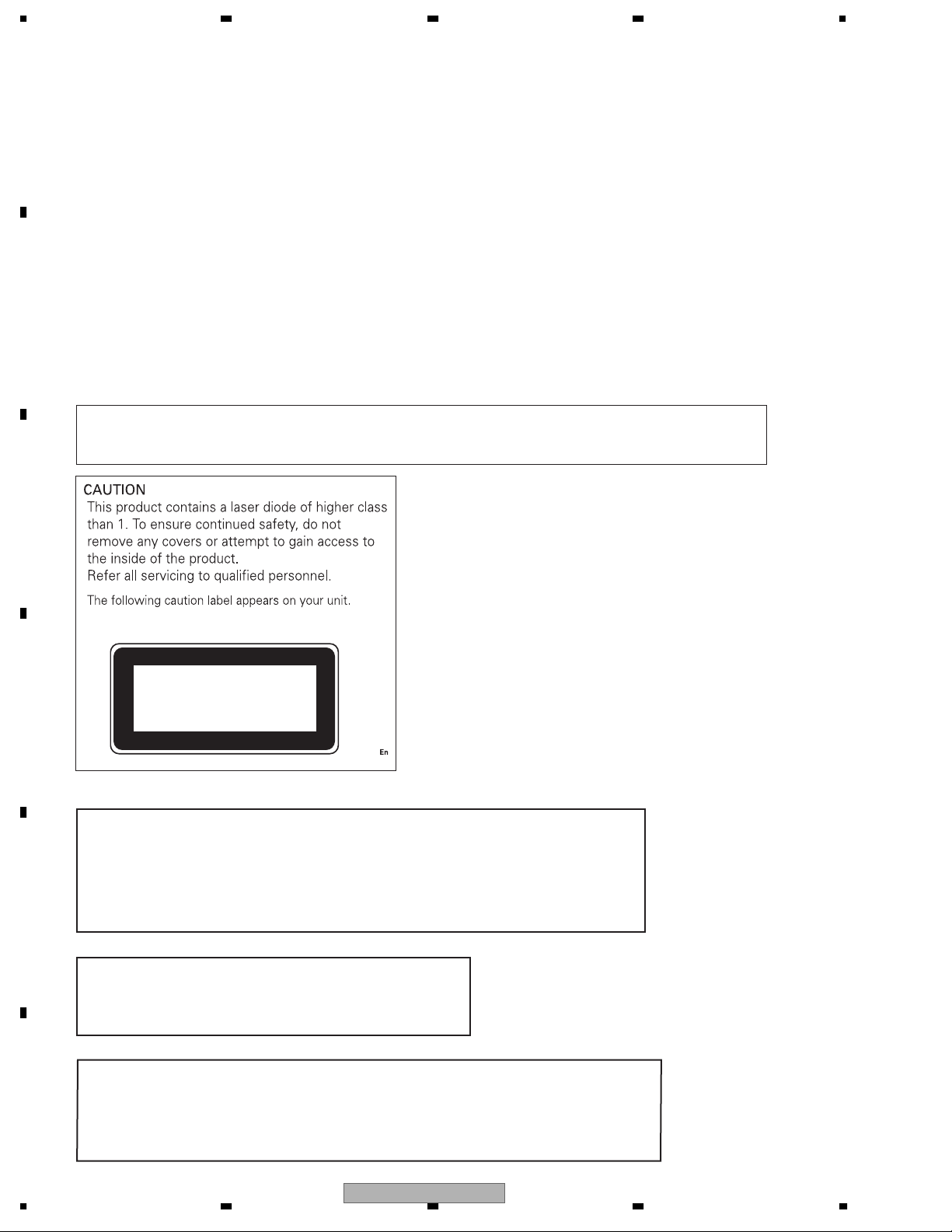
CAUTION:
USE OF CONTROLS OR ADJUSTMENTS OR PERFORMANCE OF PROCEDURES OTHER THAN THOSE
SPECIFIED HEREIN MAY RESULT IN HAZARDOUS RADIATION EXPOSURE.
C
CLASS 1
D
The AEL (accessible emission level )of the laser power output is less than CLASS 1
but the laser component is capable of emitting radiation exceeding the limit for
CLASS 1.
E
A specially instructed person should do servicing operation of the apparatus.
LASER PRODUCT
WARNING!
Laser diode characteristics
Wave length : 785 nm to 814 nm
Maximum output : 1 190 μW(Emitting period : unlimited)
Additional Laser Caution
Transistors Q101 in PCB drive the laser diodes.
F
2
When Q101 is shorted between their terminals, the laser diodes will radiate beam.
If the top cover is removed with no disc loaded while such short-circuit is continued,
the naked eyes may be exposed to the laser beam.
DEH-P5900MP/XU/EW5
1234
Page 3
5678
CAUTION
Danger of explosion if battery is incorrectly replaced.
Replaced only with the same or equivalent type recommended by the manufacture.
Discord used batteries according to the manufacture's instructions.
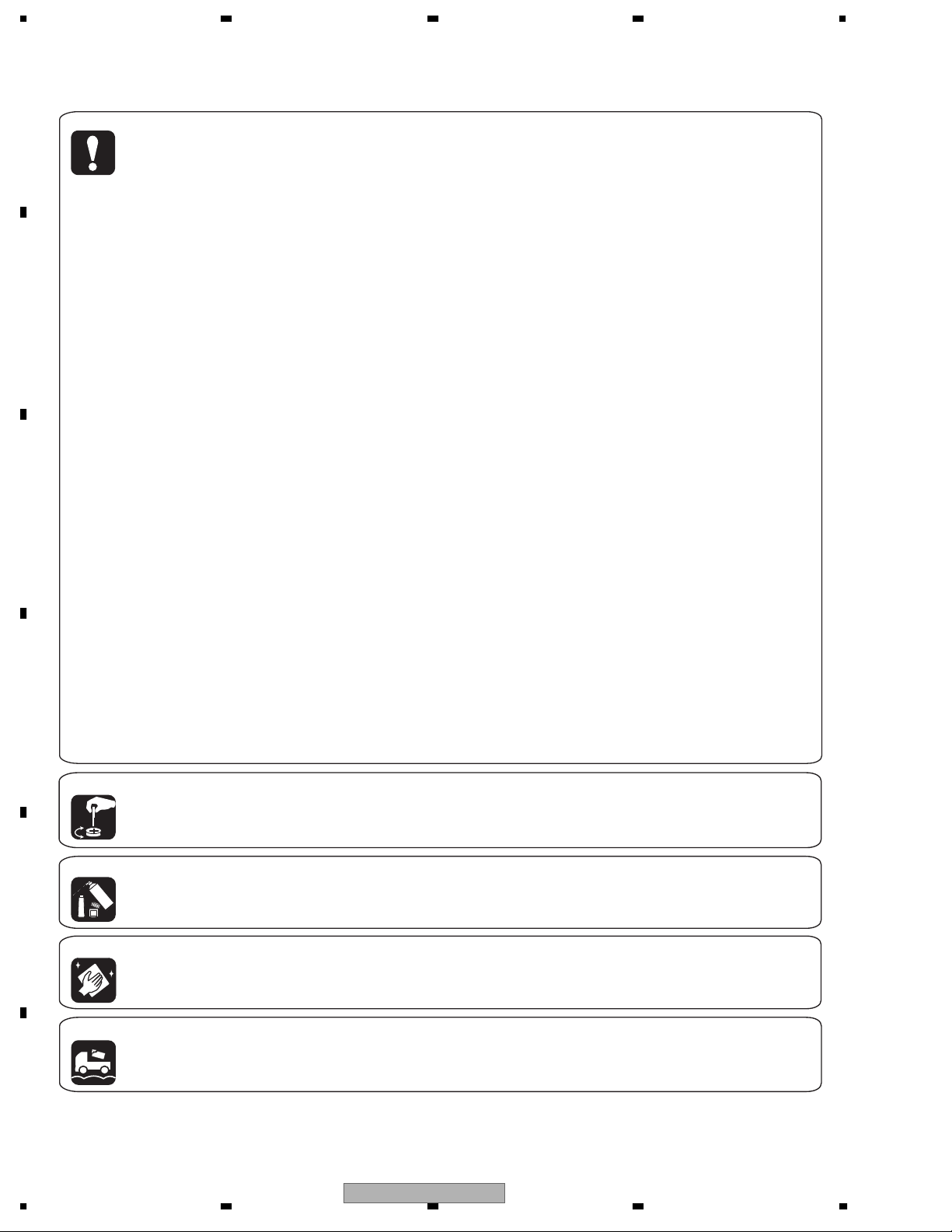
- Service Precaution
1. You should conform to the regulations governing
the product (safety, radio and noise, and other
regulations), and should keep the safety during
servicing by following the safety instructions
described in this manual.
2. Before disassembling the unit, be sure to turn off
the power. Unplugging and plugging the connectors
during power-on mode may damage the ICs inside
the unit.
3. To protect the pickup unit from electrostatic discharge
during servicing, take an appropriate treatment
(shorting-solder) by referring to "the DISASSEMBLY".
4. After replacing the pickup unit, be sure to check the
grating.
5. Be careful in handling ICs. Some ICs such as MOS
type are so fragile that they can be damaged by
electrostatic induction.
A
B
C
D
E
F
56
DEH-P5900MP/XU/EW5
7
8
3
Page 4
1234
[Important Check Points for Good Servicing]
In this manual, procedures that must be performed during repairs are marked with the below symbol.
Please be sure to confirm and follow these procedures.
A
B
C
D
1. Product safety
Please conform to product regulations (such as safety and radiation regulations), and maintain a safe servicing environment by
following the safety instructions described in this manual.
1 Use specified parts for repair.
Use genuine parts. Be sure to use important parts for safety.
2 Do not perform modifications without proper instructions.
Please follow the specified safety methods when modification(addition/change of parts) is required due to interferences such as
radio/TV interference and foreign noise.
3 Make sure the soldering of repaired locations is properly performed.
When you solder while repairing, please be sure that there are no cold solder and other debris.
Soldering should be finished with the proper quantity. (Refer to the example)
4 Make sure the screws are tightly fastened.
Please be sure that all screws are fastened, and that there are no loose screws.
5 Make sure each connectors are correctly inserted.
Please be sure that all connectors are inserted, and that there are no imperfect insertion.
6 Make sure the wiring cables are set to their original state.
Please replace the wiring and cables to the original state after repairs.
In addition, be sure that there are no pinched wires, etc.
7 Make sure screws and soldering scraps do not remain inside the product.
Please check that neither solder debris nor screws remain inside the product.
8 There should be no semi-broken wires, scratches, melting, etc. on the coating of the power cord.
Damaged power cords may lead to fire accidents, so please be sure that there are no damages.
If you find a damaged power cord, please exchange it with a suitable one.
9 There should be no spark traces or similar marks on the power plug.
When spark traces or similar marks are found on the power supply plug, please check the connection and advise on secure
connections and suitable usage. Please exchange the power cord if necessary.
0 Safe environment should be secured during servicing.
When you perform repairs, please pay attention to static electricity, furniture, household articles, etc. in order to prevent injuries.
Please pay attention to your surroundings and repair safely.
2. Adjustments
To keep the original performance of the products, optimum adjustments and confirmation of characteristics within specification.
Adjustments should be performed in accordance with the procedures/instructions described in this manual.
3. Lubricants, Glues, and Replacement parts
Use grease and adhesives that are equal to the specified substance.
E
Make sure the proper amount is applied.
4. Cleaning
For parts that require cleaning, such as optical pickups, tape deck heads, lenses and mirrors used in projection monitors, proper
cleaning should be performed to restore their performances.
5. Shipping mode and Shipping screws
To protect products from damages or failures during transit, the shipping mode should be set or the shipping screws should be
installed before shipment. Please be sure to follow this method especially if it is specified in this manual.
F
4
1234
DEH-P5900MP/XU/EW5
Page 5

5678
CONTENTS
SAFETY INFORMATION......................................................................................................................................2
1. SPECIFICATIONS .............................................................................................................................................6
2. EXPLODED VIEWS AND PARTS LIST.............................................................................................................8
2.1 PACKING....................................................................................................................................................8
2.2 EXTERIOR ...............................................................................................................................................10
2.3 CD MECHANISM MODULE .....................................................................................................................12
3. BLOCK DIAGRAM AND SCHEMATIC DIAGRAM ..........................................................................................14
3.1 BLOCK DIAGRAM....................................................................................................................................14
3.2 OVERALL CONNECTION DIAGRAM(GUIDE PAGE) ..............................................................................16
3.3 KEYBOARD UNIT ....................................................................................................................................22
3.4 CD MECHANISM MODULE(GUIDE PAGE).............................................................................................24
4. PCB CONNECTION DIAGRAM ......................................................................................................................32
4.1 TUNER AMP UNIT ...................................................................................................................................32
4.2 KEYBOARD UNIT ....................................................................................................................................36
4.3 PANEL UNIT.............................................................................................................................................37
4.4 CD CORE UNIT(S10.5COMP2) ...............................................................................................................38
5. ELECTRICAL PARTS LIST .............................................................................................................................40
6. ADJUSTMENT ................................................................................................................................................46
6.1 CD ADJUSTMENT ...................................................................................................................................46
6.2 CHECKING THE GRATING AFTER CHANGING THE PICKUP UNIT.....................................................48
6.3 ERROR MODE.........................................................................................................................................50
6.4 SYSTEM MICROCOMPUTER TEST PROGRAM....................................................................................51
7. GENERAL INFORMATION .............................................................................................................................52
7.1 DIAGNOSIS..............................................................................................................................................52
7.1.1 DISASSEMBLY......................................................................................................................................52
7.1.2 CONNECTOR FUNCTION DESCRIPTION ..........................................................................................55
7.2 PARTS ......................................................................................................................................................56
7.2.1 IC ...........................................................................................................................................................56
7.2.2 DISPLAY................................................................................................................................................65
7.3 OPERATIONAL FLOW CHART................................................................................................................66
8. OPERATIONS .................................................................................................................................................67
A
B
C
D
E
F
56
DEH-P5900MP/XU/EW5
7
8
5
Page 6
1234
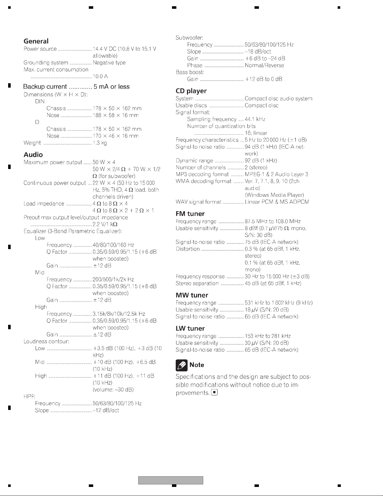
1. SPECIFICATIONS
A
B
C
D
E
F
6
1234
DEH-P5900MP/XU/EW5
Page 7

5678
A
B
C
D
E
56
DEH-P5900MP/XU/EW5
F
7
8
7
Page 8
N
1234
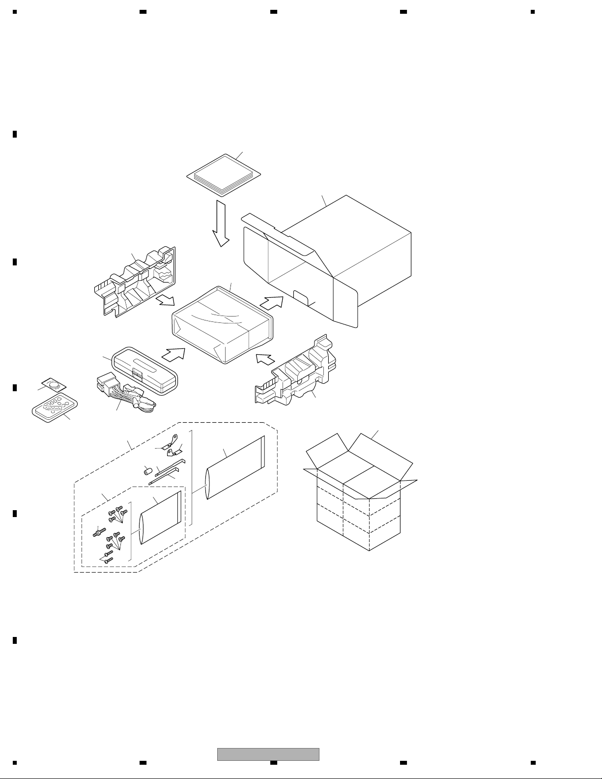
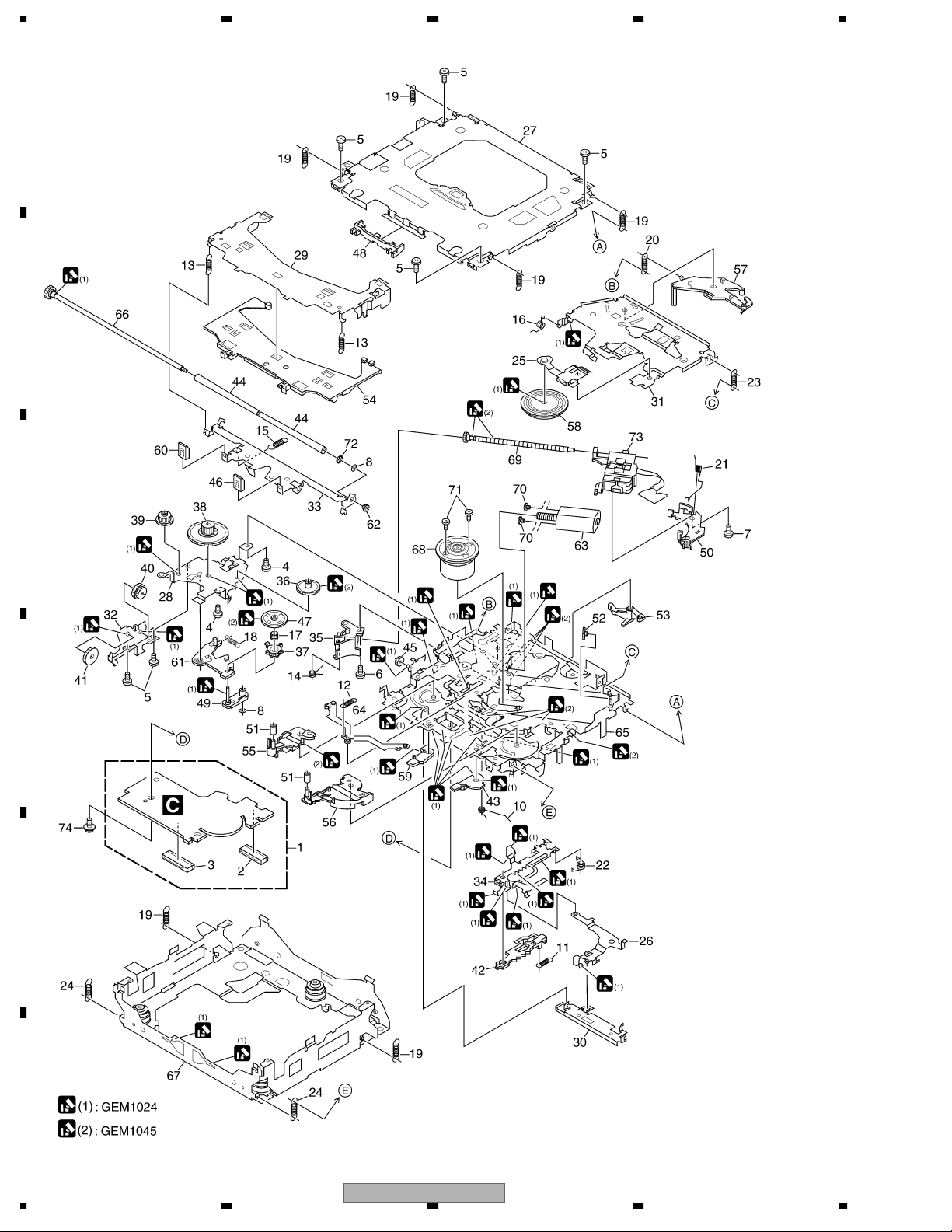
2. EXPLODED VIEWS AND PARTS LIST
OTES : • Parts marked by " * " are generally unavailable because they are not in our Master Spare Parts List.
• The > mark found on some component parts indicates the importance of the safety factor of the part.
A
Therefore, when replacing, be sure to use parts of identical designation.
• Screw adjacent to mark on the product are used for disassembly.
• For the applying amount of lubricants or glue, follow the instructions in this manual.
(In the case of no amount instructions,apply as you think it appropriate.)
2.1 PACKING
"
22
B
C
D
DEH-P5900MP/XU/EW5packing
21
4
3
5
1
6
11
2
8
9
10
7
18
20
19
12
14
13
E
F
8
1234
15
17
16
10
DEH-P5900MP/XU/EW5
Page 9
5678
PACKING SECTION PARTS LIST
Mark No. Description Part No.
1 Cord Assy CDP1015
2 Polyethylene Bag CEG-162
* 3 Battery CEX1065
4 Case Assy CXB3520
5 Remote Control Assy CXC5719
* 6 Accessory Assy YEA5014
* 7 Polyethylene Bag CEG-158
8 Holder(L) CND1249
9 Holder(R) CND1250
10 Handle CND3707
11 Bush CNV3930
12 Screw Assy YEA5007
13 Screw BPZ20P060FTB
14 Screw CBA1650
Owner's Manual,Installation Manual
Part No. Language
Mark No. Description Part No.
* 15 Polyethylene Bag CEG-127
16 Screw CRZ50P090FTC
17 Screw TRZ50P080FTC
18 Carton YHG5105
19 Contain Box YHL5095
20 Protector YHP5008
21 Protector YHP5009
22-1 Owner's Manual YRD5106
22-2 Owner's Manual YRD5107
22-3 Owner's Manual YRD5108
22-4 Installation Manual YRD5109
* 22-5 Warranty Card CRY1157
A
B
YRD5106 English, Spanish
YRD5107 German, French
YRD5108 Italian, Dutch, Russian
YRD5109 English, Spanish, German, French, Italian, Dutch, Russian
C
D
E
56
DEH-P5900MP/XU/EW5
F
7
8
9
Page 10
1234
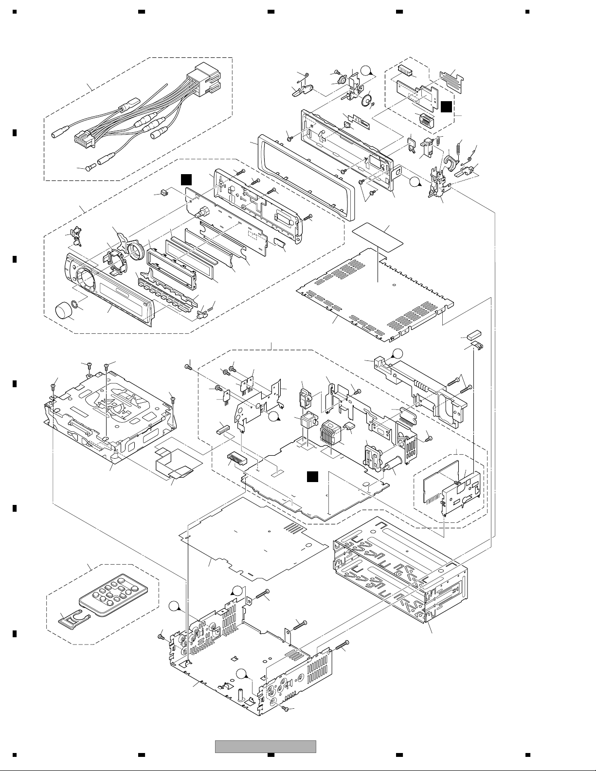
2.2 EXTERIOR
55
71
33
15
56
62
20
24
69
22
64
17
56
23
A
57
72
75
74
54
67
C
76
81
D
79
20
19
58
65
56
36
36
46
32
31
25
B
A
B
C
D
53
6
18
45
43
41
21
77
37
21
27
47
36
77
21
50
36
49
78
7
B
35
44
39
42
52
38
2
2
80
51
48
40
2
4
2
70
D
60
68
10
29
63
8
3
73
61
59
66
13
14
11
E
12
F
10
1234
B
1
34
26
16
D
5
C
DEH-P5900MP/XU/EW5
A
5
5
DEH-P5900MP/XU/EW5
1
28
9
30
Page 11

>
5678
EXTERIOR SECTION PARTS LIST
Mark No. Description Part No.
1 Screw BMZ30P040FTB
2 Screw BSZ26P060FTC
3 Screw BSZ26P200FTC
4 Screw BSZ30P060FTC
5 Screw BSZ30P200FTC
6 Cord Assy CDP1015
7 Cap CKX-003
8 Earth Plate CNC8915
9 Holder CND3598
10 Cushion CNM8890
11 Remote Control Assy CXC5719
12 Cover CNS7068
13 CD Mechanism Module(S10.5) CXK5760
14 Cable YDE5025
15 Case YNB5014
16 Insulator YNM5062
17 Heat Sink YNR5031
18 Panel YNS5175
19 Tuner Amp Unit YWM5145
20 Screw BPZ26P070FTC
21 Screw BSZ26P060FTC
22 Fuse(10 A) CEK1208
23 Pin Jack(CN351) CKB1051
24 Plug(CN901) CKM1376
25 Connector(CN101) CKS3408
26 Plug(CN801) CKS3537
27 Connector(CN701) CKS3829
28 Antenna Jack(CN401) CKX1056
29 FM/AM Tuner Unit CWE1951
30 Holder CND1054
31 Holder XNC7030
32 Jack(CN621) YKS5001
33 Holder YNC5041
34 Chassis Unit YXA5201
35 Detachable Assy YXA5218
Mark No. Description Part No.
50 Lighting Conductor YNV5083
51 Connector YNV5084
52 Grille Assy YXA5202
53 Button Unit(ILL/BAND) YXA5215
54 Button(EJECT) CAC7752
55 Screw(M2 x 4) CBA1649
56 Screw(M2 x 4.5) CBA1925
57 Washer CBF1038
58 Spring CBH2650
59 Spring CBH2651
60 Spring CBH2652
61 Spring CBH2653
62 Spring CBL1512
63 Holder CND1254
64 Pin CNV6486
65 Arm CNV7400
66 Arm CNV7401
67 Arm CNV7402
68 Arm CNV7403
69 Holder Unit CXB9501
70 Holder Unit CXB9502
71 Damper Unit CXB9503
72 Gear YNV5053
73 Panel Unit YWM5148
74 Connector(CN1901) CKS4806
75 Connector(CN1902) CKS5192
76 Sub Panel Unit YXA5242
77 Transistor (Q702,Q911) 2SD2396
78 IC(IC921) NJM2388F84
79 IC(IC301) PAL007C
80 IC(IC1802) BU2507FV
* 81 Label CRW1541
A
B
C
D
36 Screw BPZ20P080FTB
37 Spring CBH2210
38 Knob(SOURCE, VOLUME) YAA5015
39 Button(UP/DOWN/L/R) YAC5177
40 Button(1-6) YAC5179
41 Button(OPEN) YAC5180
42 Spring YBH5003
43 Cover YNS5174
44 Lighting Conductor YNV5085
45 Lighting Conductor YNV5086
46 Connector(CN1801) CKS5207
47 LCD(LCD1801) YAW5082
48 Holder YNC5040
49 Reflect Sheet YNM5066
56
DEH-P5900MP/XU/EW5
E
F
7
8
11
Page 12
1234
2.3 CD MECHANISM MODULE
A
B
C
D
E
F
12
1234
DEH-P5900MP/XU/EW5
Page 13

5678
CD MECHANISM MODULE SECTION PARTS LIST
Mark No. Description Part No.
1 CD Core Unit(S10.5COMP2) CWX3350
2 Connector(CN101) CKS4911
3 Connector(CN701) CKS4808
4 Screw BMZ20P025FTC
5 Screw BSZ20P040FTC
6 Screw(M2 x 3) CBA1511
7 Screw(M2 x 4) CBA1835
8 Washer CBF1038
9 •••••
10 Spring CBH2609
11 Spring CBH2612
12 Spring CBH2614
13 Spring CBH2616
14 Spring CBH2617
15 Spring CBH2620
16 Spring CBH2855
17 Spring CBH2937
18 Spring CBH2735
19 Spring CBH2854
20 Spring CBH2642
21 Spring CBH2856
22 Spring CBH2857
23 Spring CBH2860
24 Spring CBH2861
25 Spring CBL1686
26 Arm CND1909
27 Frame CND2582
28 Bracket CND2583
29 Arm CND2584
30 Lever CND2585
Mark No. Description Part No.
50 Rack CNV8342
51 Roller CNV8343
52 Holder CNV8344
53 Arm CNV8345
54 Guide CNV8347
55 Arm CNV8348
56 Arm CNV8349
57 Arm CNV8350
58 Clamper CNV8365
59 Arm CNV8386
60 Guide CNV8396
61 Arm CNV8413
62 Collar CNV8447
63 Motor Unit(M2) CXC4026
64 Arm Unit CXC4027
65 Chassis Unit CXC4028
66 Gear Unit CXC4029
67 Frame Unit CXC4031
68 Motor Unit(M1) CXC7134
69 Screw Unit CXC6359
70 Screw JFZ20P020FTC
71 Screw JGZ17P022FTC
72 Washer YE20FTC
73 Pickup Unit(P10.5)(Service) CXX1942
74 Screw IMS26P030FTC
A
B
C
D
31 Arm CND2586
32 Bracket CND2587
33 Arm CND2588
34 Lever CND2589
35 Holder CNV7201
36 Gear CNV7207
37 Gear CNV7208
38 Gear CNV7209
39 Gear CNV7210
40 Gear CNV7211
41 Gear CNV7212
42 Rack CNV7214
43 Arm CNV7216
44 Roller CNV8189
45 Gear CNV7219
46 Guide CNV7361
47 Gear CNV7595
48 Guide CNV8448
49 Arm CNV7805
56
DEH-P5900MP/XU/EW5
E
F
7
8
13
Page 14
_
−
+
_
C
O
2
T
T
C
T
C
_
S
L
1234
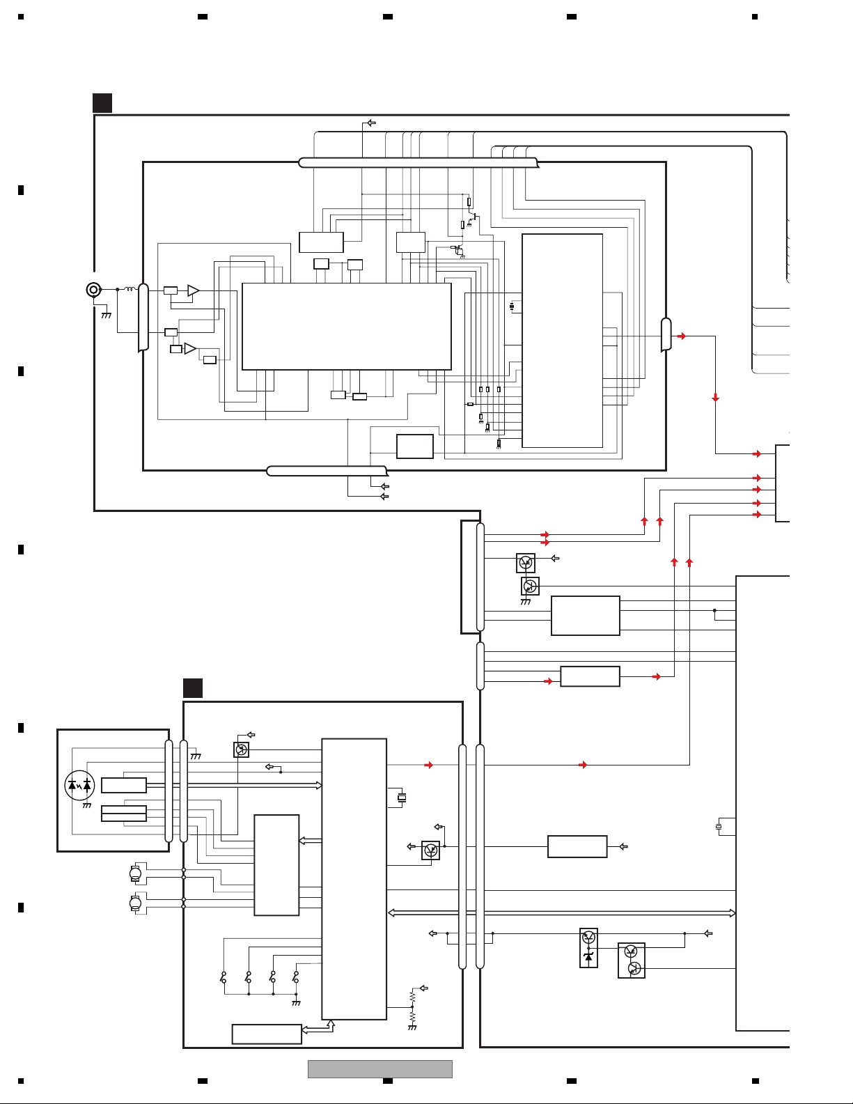
3. BLOCK DIAGRAM AND SCHEMATIC DIAGRAM
3.1 BLOCK DIAGRAM
A
B
C
D
E
F
ANTENNA
PICKUP UNIT
(P10.5)(SERVICE)
LASER
DIODE
MONITOR
DIODE
LOAD/
TUNER AMP UNIT
A
FM/AM TUNER UNIT
CN401
1
2
TRACKING ACT.
SPINDLE
MOTOR
CARRIAGE
MOTOR
HOLOGRAM
UNIT
FOCUS ACT.
AM ANT
1
FM ANT
3
LD-
MD
VREF
FOM
FOP
TOP
TOM
LD+
M
M
FMRF
ATT
ATT
FMRF
RF adj
ANT adj
CD CORE UNIT(S10.5COMP2)
C
D
Q101
S905
8EJ
S-93C56BD0I-J8
VDD
REFO
12
FOM
11
FOP
14
TOP
13
TOM
16
SOP
15
SOM
18
LCOP
17
LCOM
EEPROM
IC202
AC,BD,F,E
DRIVER
BA5839FP
DSCSNS
CN101
15
15
5
5
88
FOM
33
FOP
2
2
TOP
1
1
TOM
44
14
14
S904
12EJ
VDD5
CE1
TUNPCK
DI
CK
CE1
IC5
←
IC4
←
2.5V
CN701
LOUT
X201
16.93MHz
VDD
Q102
/RESET
BRST,BRXEN,BSRQ
VD
VD
LDET
VDD
VD
SL
VDD_3.3
LOUT
XTAL
/XTAL
/PUEN
/RESET
VDSENS
SL
3.3V
VDD_3.3V
VCC8
55
50
52
39
16
11
TUNPDI
5V 3.3V
3.3V 2.5V
VCC
BDATA,BSCK
CE2
76 13 5 1098 11 14 18192021
NC
CE2
ROM_VDD
IC3 EEPROM
5.0V
OSC
LPF
IC1
3.3V
MIXER, IF AMP
T51
CF52
RFGND
OSCGND
DGND
212 1522 16 4 17
AUDIOGNDNCVCC
RF-AMP, CD DECODER,
MP3/WMA DECODER,
DIGITAL SERVO /
DATA PROCESSOR
141
LD
142
PD
133
REFOUT
CD
IC301
S903
LOEJ
CLCONT
CONT
22
21
9
S901
HOME
TD,FD
SD,MD
CS,SK
DI,DO
43
41
5
8
7
6
9
LOEJ
CLCONT
CONT
12EJ
8EJ
DSCSNS
HOME
IC201
PE5547A
LDET
TUNPDO
DO
CN101
IN1−
11
IN1+
7
B14
8
IP_BUS
5
1
CN621
KEY2
2
KEY1
3
AUX-GND
4
AUX-L
5
CN701
LOUT
13
13
9
9
RESET
8
8
VD
1
1
2
2
RDS_CK
RDS_DATA
RDS_HSLK
RDS_LOCK
IC2
2.5V
DET, FM MPX,
RDS DECODER
Q101
Q102
5
6
10,12
B.UP
HA12241FP
14
CD 3V REGULATOR
3
NJM2885DL1-33
BRST,BRXEN,BSRQ,BDATA,BSCK
IC101
IC751
NJM2794V
IC702
Q702
RDS_CK
RDS_HSLK
TUNL
BUSL-
BUSL+
AUX-L
CDL
40
30
29
27
52
94
34
RDS_LOCK
RDS_DATA
ASENBO
TX
RX
RX2
IPPW
KEYAD
KEYD
SYSTEM CO
ELE
2
5
4
3
1
IC601
PEG
S
IN2
IN4
IN4
IN3
IN1
Lch
23
1
2
8
1
13
Xout
X601
15
B.UP
Xin
21
CDRST
22
VCCONT
1
VDD5
Q701
5
14
1234
DEH-P5900MP/XU/EW5
Page 15
TUNL
0
BUSL-
BUSL+
AUX-L
CDL
5678
A
CN351
4
B.UP
SYSPW
Q351
Q353
SWL
RCFL
CN901
B.UP
ACC
FL−
FL+
RL−
RL+
BREM
TEL
6
B
1
1
3
3
2
2
10
10
12
12
9
9
11
11
6
6
8
8
BACK
GND
BACK UP
ACC
GND
FL−
FL+
RL−
RL+
B.REM
RR
RR
+
−
FR
REM
ACC
FR
+
−
B.
FL
FL
+
−
RL
RL
+
−
UP
C
D
RESET
12
IC961
S-80835CNMC-B8U
12
68
TPDI
86
TPDO
75
LDET
67
TPCK
66
TUNPCE1
65
TUNPCE2
97
SL
SYSTEM CONTROLLER
74
RCK
83
RDS57K
81
RDSLOCK
82
RDSDT
Front_L
Pre/SW_L
Rear_L
53
MUTE
48
38
TELIN
26
PEE
/RESET
6
12
7
IC601(1/2)
PEG284A
BUZZER
BZ601
TUNPDO
TUNPDI
LDET
TUNPCK
CE1
CE2
SL
Q401
RDS_CK
RDS_HSLK
Q402
RDS_LOCK
RDS_DATA
ELECTRONIC VOLUME/
SOURCE SELECTOR
2
IN2_L
5
IN4−_L
4
IC151
IN4+_L
PML015B
3
IN3_L
1
IN1_L
40
ASENBO
30
TX
29
RX
27
RX2
52
IPPW
94
KEYAD
34
KEYD
VCK, VDT, VST
SYSPW
DALMON
/BSENS
/ASENS
B.UP
VDD5
VDD5V REGULATOR
VDD5
47
19
20
/BSENS
/ASENS
Q911
BACKUP SENSE
Q931
Q912
B.UP
ACC SENSE
B.UP
6
20
Vcc Vcc
IC301
PAL007C
B.REM
STBY
4
SYS 8V REGULATOR
NJM2388F84
FL−
FL+
RL−
RL+
IC921
4
SYSPW
23
21
3
5
25
1213
MUTE
Q453
Q451
VCC8
VDD_3.3V
14
12
22
TUN 3V REGULATOR
IC401
NJM2885DL1-33
TEL IN
Q951
POWER AMP
FLIN
RLIN
MUTE
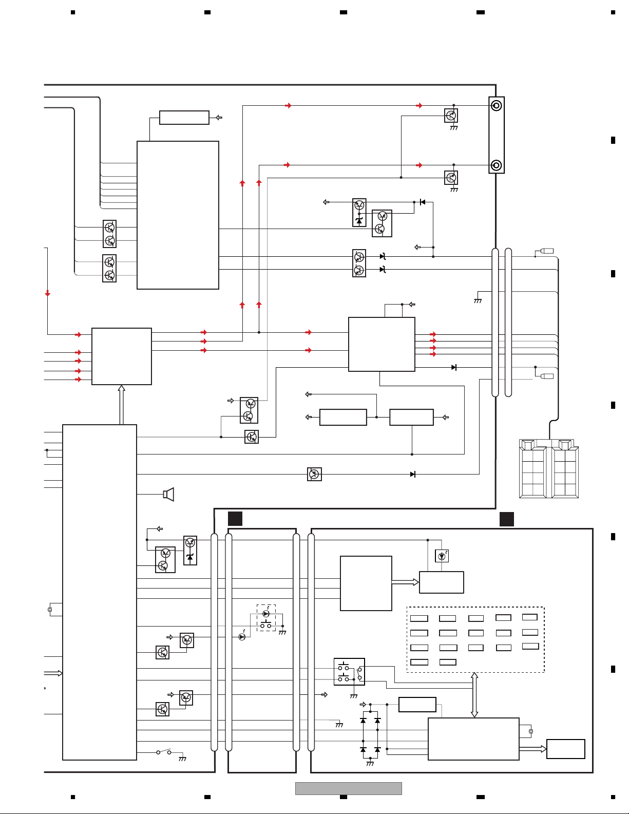
SYSTEM CONTROLLER
IC601(2/2)
PEG284A
ILMPW
DADT
DACLK
13
Xout
1
15
Xin
21
CDRST
B.UP
22
VCCONT
DAST
/EJTIN
FLPILM
ROT1
ROT0
SWVDD
CSENS
DPDT
KYDT
/DSENS
B.UP
Q843
1
91
89
90
2
B.UP
Q801
6
3
4
VDD5
Q852
7
93
35
36
S801
18
Q802
Q851
Q844
CN801
BKLT
DADT
DACLK
DAST
EJECT
FLPILM
ROT1
ROT0
SWVDD
CSENS
DPDT
KYDT
8
14
9
13
12
10
7
6
3
11
5
4
56
D
8
14
9
13
12
10
7
6
3
11
5
4
CN1902
PANEL UNIT
CN1901
ILMB+
DADT
DACLK
DAST
S1901
4
2
ROT1
ROT0
SWVDD
CSENS
DPDT
KYDT
CN1801
ILMB+
9
9
IC1802
BU2507FV
12
DADT
12
12
4
4
11
11
6
6
7
7
5
5
3
3
8
8
10
10
DACLK
DAST
ROT1
ROT0
CSENS
DPDT
KYDT
11
10
1
2
SWVDD
DI
CLK
LD
S1821
SWVDD
4
KST3
KDT3
5
3
DEH-P5900MP/XU/EW5
A01-A06
REM.CON.
IC1803
3
GP1UX51RK
7
S1801
S1807
LEFT
S1812
S1817
1
ILL
TA
Q1801-Q1814
LED DRIVE
50
SI
49
SO
46
V3
47
VDD
(RGB)
KEY MATRIX
S1803
DOWN
S1808
3
S1813
RIGHT
S1818
6
1
57
REM
LCD DRIVER/
KEY CONTROLLER
PD6538A
S1804
2
S1809
AUDIO
S1814
FUNC
KEY DATA
IC1801
KDT1-4,KST1-5
KEYBOARD UNIT
B
S1806
S1805
DISP
BAND
S1811
S1810
S1815
4
UP
S1816
EQ
5
54
X0
55
X1
X1801
5MHz
8
E
F
LCD1801
15
Page 16
A-a
A-b
A-a
A-b
A-b
A-a
1234
3.2 OVERALL CONNECTION DIAGRAM(GUIDE PAGE)
Note: When ordering service parts, be sure to refer to " EXPLODED VIEWS AND PARTS LIST" or
"ELECTRICAL PARTS LIST".
A
Large size
A-b
A-b
SCH diagram
Guide page
FM(10%) : -29.5 dB
AM(15%) : -26.0 dB
A-a
A-a
A-a
CD(-20 dB) : -19.4 dB
CN701
C
A-b
Detailed page
A-a
B
FM/AM TUNER UNIT
ANTENNA
C
15MHz
CSS1653
AUX IN
AUX IN(-20 dB) : -17.8 dB
SYSTEM
CONTROLLER
D
E
F
A D
IP-BUS(-20 dB) : -17.8 dB
B
CN1801
D842
S5688G
BKLT
EJECT
PANEL UNIT
D
DSENS
16
1234
DEH-P5900MP/XU/EW5
Page 17
5678
INPUT FM : -33.1 dB
AM : -29.6 dB
CD : -22.4 dB
IP-BUS : -20.8 dB
AUX IN : -20.8 dB
OUTPUT FM : -12.0 dB
AM : -8.5 dB
CD : -8.3 dB
IP-BUS : -8.7 dB
AUX IN : -8.7 dB
A-b
TUNER AMP UNIT
A
3A
3300/16
A
FRONT
R CH
SUB WOOFER
R CH
FRONT
L CH
G
SUB WOOFER
L CH
B
C
CEK1208
10A
R
D
RR
RR
+
-
BACK
FR
FR
UP
+
-
B.
FL
FL
REM
+
RL
RL
ACC
GND
+
-
DSENS
D842
S5688G
NOTE :
Symbol indicates a resistor.
No differentiation is made between chip resistors and
discrete resistors.
Symbol indicates a capacitor.
No differentiation is made between chip capacitors and
discrete capacitors.
For resistors and capacitors in the circuit diagrams, their resistance values or
capacitance values are expressed in codes:
Ex. *Resistors
Code Practical value
123 12k ohms
103 10k ohms
*Capacitors
Code Practical value
103 0.01uF
101/10 100uF/10V
The mark found on some component parts indicates
the importance of the safety factor of the part.
Therefore, when replacing, be sure to use parts of
identical designation.
FM : 13.98 dB
AM : 17.48 dB
CD : 17.7 dB
IP-BUS : 17.3 dB
AUX IN : 17.3 dB
E
F
A
56
DEH-P5900MP/XU/EW5
7
8
17
Page 18
1234
A
B
FRONT
R CH
SUB WOOFER
R CH
FRONT
L CH
G
SUB WOOFER
L CH
CEK1208
10A
3300/16
3A
TUNER AMP UNIT
A
C
A-a A-b
D
INPUT FM : -33.1 dB
AM : -29.6 dB
CD : -22.4 dB
IP-BUS : -20.8 dB
AUX IN : -20.8 dB
OUTPUT FM : -12.0 dB
AM : -8.5 dB
CD : -8.3 dB
IP-BUS : -8.7 dB
E
AUX IN : -8.7 dB
F
A-b
18
1
2
DEH-P5900MP/XU/EW5
1234
Page 19
5678
+
+
+
+
RL
FL
FR
RR
RR
-
-
-
-
RL
FL
FR
B.
REM
ACC
UP
GND
BACK
FM : 13.98 dB
AM : 17.48 dB
CD : 17.7 dB
IP-BUS : 17.3 dB
AUX IN : 17.3 dB
A
B
The mark found on some component parts indicates
the importance of the safety factor of the part.
Therefore, when replacing, be sure to use parts of
identical designation.
Symbol indicates a resistor.
No differentiation is made between chip resistors and
discrete resistors.
Symbol indicates a capacitor.
No differentiation is made between chip capacitors and
NOTE :
discrete capacitors.
For resistors and capacitors in the circuit diagrams, their resistance values or
capacitance values are expressed in codes:
A-a A-b
Ex. *Resistors
Code Practical value
123 12k ohms
103 10k ohms
*Capacitors
Code Practical value
103 0.01uF
101/10 100uF/10V
C
D
E
3
4
5
8G
6
DEH-P5900MP/XU/EW5
56
F
7
7
A-b
8
19
Page 20
1234
A
B
C
A-b
1
CN701
C
2
CSS1653
15MHz
SYSTEM
CONTROLLER
CD(-20 dB) : -19.4 dB
A-bA-a
D
E
FM(10%) : -29.5 dB
AM(15%) : -26.0 dB
F
A-a
20
AUX IN(-20 dB) : -17.8 dB
FM/AM TUNER UNIT
ANTENNA
DEH-P5900MP/XU/EW5
1234
AUX IN
Page 21
5678
SYSTEM
CONTROLLER
3
4
5
D842
S5688G
6
DSENS
7
A-b
A
B
C
AUX IN(-20 dB) : -17.8 dB
A-bA-a
EJECT
D
PANEL UNIT
D
BKLT
E
B
CN1801
IP-BUS(-20 dB) : -17.8 dB
56
DEH-P5900MP/XU/EW5
F
A-a
7
8
D
21
Page 22

1234
3.3 KEYBOARD UNIT
A
SOURCE/
VOLUME
B
D
CN1901
C
LCD DRIVER/
KEY CONTROLLER
D
E
F
B
22
1234
DEH-P5900MP/XU/EW5
Page 23

5678
A
KEYBOARD UNIT
B
B
C
D
E
56
DEH-P5900MP/XU/EW5
F
B
7
8
23
Page 24

1234
3.4 CD MECHANISM MODULE(GUIDE PAGE)
A
PICKUP UNIT(P10.5)(SERVICE)
B
C-a
F
T
F
T
F
F
T
T
C
%
F
F
T
T
#
@
F
F
T
T
EEPROM
SWITCHES:
CD CORE UNIT(S10.5COMP2)
S901:HOME SWITCH..........ON-OFF
S903:DSCSNS SWITCH......ON-OFF
S904:12EJ SWITCH.............ON-OFF
S905:8EJ SWITCH...............ON-OFF
The underlined indicates the switch position.
D
M1 CXC7134
SPINDLE MOTOR
M2 CXC4026
LOADING/CARRIAGE MOTOR
E
S
S
C
C
T
9
F
0
$
S
7
C
4
8
5
3
2
1
CD DRIVER
F
C
24
1234
DEH-P5900MP/XU/EW5
Page 25

5678
A
C-b
CD CORE UNIT(S10.5COMP2)
C
!
SIGNAL LINE
F
FOCUS SERVO LINE
T
TRACKING SERVO LINE
C
CARRIAGE SERVO LINE
S
SPINDLE SERVO LINE
B
C
D
56
DEH-P5900MP/XU/EW5
A
CN701
6
E
&^
F
C
7
8
25
Page 26

1234
A
B
C
SIGNAL LINE
FOCUS SERVO LINE
TRACKING SERVO LINE
CARRIAGE SERVO LINE
SPINDLE SERVO LINE
F
T
S
C
CD CORE UNIT(S10.5COMP2)
C
C-a C-b
D
E
F
C-b
26
!
1
DEH-P5900MP/XU/EW5
1234
Page 27

5678
A
A
CN701
6
B
&^
C
C-a C-b
D
E
2 3
DEH-P5900MP/XU/EW5
56
F
C-b
7
8
27
Page 28

A
S905:8EJ SWITCH ON-OFF
B
C-b
1234
1
FFT
T
#
%
FFT
T
@
EEPROM
C
C-bC-a
D
FFT
T
E
F
C-a
28
FFT
T
SWITCHES:
CD CORE UNIT(S10.5COMP2)
S901:HOME SWITCH..........ON-OFF
S903:DSCSNS SWITCH......ON-OFF
PICKUP UNIT(P10.5)(SERVICE)
S904:12EJ SWITCH.............ON-OFF
DEH-P5900MP/XU/EW5
1234
Page 29

EEPROM
5678
A
2 3
4
5
8
7
$
C
S
C-b
B
C
CD DRIVER
c-bC-a
9
0
F
T
S
S
C
C
3
2
1
D
E
SWITCHES:
CD CORE UNIT(S10.5COMP2)
S901:HOME SWITCH..........ON-OFF
S903:DSCSNS SWITCH......ON-OFF
S904:12EJ SWITCH.............ON-OFF
S905:8EJ SWITCH...............ON-OFF
The underlined indicates the switch position.
56
M1 CXC7134
SPINDLE MOTOR
M2 CXC4026
LOADING/CARRIAGE MOTOR
DEH-P5900MP/XU/EW5
F
C-a
7
8
29
Page 30

1234
- Waveforms Note : 1. The encircled numbers denote measuring points in the circuit diagram.
2. Reference voltage REFO1(1.65 V)
A
1DSCSNS
28SNS
312SNS
4LOEJ
12 cm CD Loading operation 12 cm CD Loading operation 8 cm CD Loading operation
5 V/div
5 V/div
5 V/div
5 V/div
500 ms/div
1DSCSNS
5CLCONT
4LOEJ
6VD
5 V/div
5 V/div
10 V/div
500 ms/div5 V/div
28SNS
312SNS
4LOEJ
5 V/div
5 V/div
5 V/div
5 V/div
500 ms/div1DSCSNS
Ref.:
GND
Mode:
Normal
B
7SIN
8CIN
9TIN
12 cm CD-DA setup operation after loading
Ref.:
C
REFO
Mode:
Normal
1 V/div
500 mV/div
1 V/div
500 mV/div
0FIN
@TE
9TIN
CD-DA Play operation Spindle waveform during play operation Spindle waveform during play operation
D
500 mV/div
500 mV/div
500 mV/div
1 s/div
20 ms/div#FE
Ref.:
GND
Mode:
Normal
!
RFOK(MONI_2)
7SIN
Ref.:
REFO
Mode:
Normal
7SIN
200 mV/div
2 V/div
2 V/div
2 V/div
500 mV/div
500 ms/div0FIN
200 ms/div$MDX
Ref.:
GND
Mode:
Normal
#FE
Source On setup operation12 cm CD-DA Source On setup operation
Ref.:
REFO
Mode:
Normal
7SIN
(Wider)
500 mV/div
500 mV/div
2 V/div
500 mV/div
200 ms/div@TE
5 μs/div$MDX
Ref.:
REFO
Mode:
Normal
500 mV/div
#FE
E
Focus Search waveform Track Open waveform 1 Track Jump waveform
Ref.:
REFO
Mode:
TEST
F
30
500 mV/div
1234
200 ms/div0FIN
Ref.:
REFO
Mode:
Normal
500 mV/div
%RFAGC
Ref.:
REFO
Mode:
TEST
500 mV/div
DEH-P5900MP/XU/EW5
2 ms/div@TE
Ref.:
REFO
Mode:
Normal
@TE
9TIN
Ref.:
REFO
Mode:
TEST
1 V/div
500 mV/div
500 mV/div
500 μs/div%RFAGC
Page 31

5678
1 V/div
@TE
9TIN
4 Tracks Jump waveform 10 Tracks Jump waveform 32 Tracks Jump waveform
Ref.:
REFO
Mode:
TEST
500 mV/div
500 mV/div
1 V/div
@TE
8CIN
7SIN
Search operation(Outter to Inner)
Ref.:
REFO
Mode:
Normal
1 V/div
1 V/div
2 V/div
500 μs/div%RFAGC
@TE
9TIN
Ref.:
REFO
Mode:
TEST
200 ms/div%RFAGC
&ROUT
Ref.:
AGND
Mode:
Normal
1 V/div
500 mV/div
500 mV/div
1 V/div
1 V/div
500 μs/div%RFAGC
@TE
9TIN
Ref.:
REFO
Mode:
TEST
200 μs/div^LOUT
28SNS
312SNS
4LOEJ
12 cm CD Eject operationAnalog audio waveform
Ref.:
GND
Mode:
Normal
1 V/div
500 mV/div
500 mV/div
5 V/div
5 V/div
5 V/div
5 V/div
2 ms/div%RFAGC
A
B
500 ms/div1DSCSNS
C
5 V/div
5CLCONT
4LOEJ
12 cm CD Eject operation 8 cm CD Eject operation Black dot(800 μm) during play
Ref.:
GND
Mode:
Normal
5 V/div
5 V/div
500 ms/div1DSCSNS
28SNS
312SNS
4LOEJ
Ref.:
GND
Mode:
Normal
5 V/div
5 V/div
5 V/div
5 V/div
500 ms/div1DSCSNS
9TIN
@TE
0FIN
Ref.:
REFO
Mode:
Normal
1 V/div
1 V/div
1 V/div
1 V/div
500 μs/div%RFAGC
D
E
56
DEH-P5900MP/XU/EW5
F
7
8
31
Page 32

1234
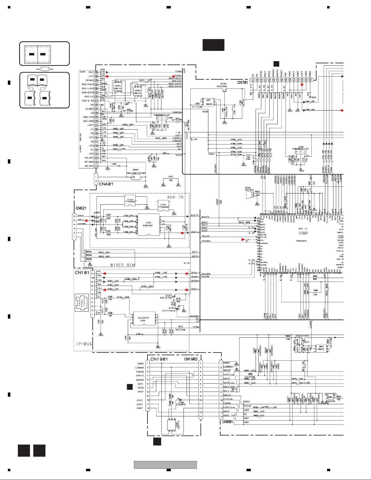
4. PCB CONNECTION DIAGRAM
4.1 TUNER AMP UNIT
A
B
C
NOTE FOR PCB DIAGRAMS
1.The parts mounted on this PCB
include all necessary parts for
several destination.
For further information for
respective destinations, be sure
to check with the schematic dia gra m.
2.Viewpoint of PCB diagrams
Connector
P.C.Board
Capacitor
Chip Part
SIDE A
SIDE B
TUNER AMP UNIT
A
AUX
WIRED REMOTE INPUT
CORD ASSY
IP-BUS INPUT
D
C
CN701
E
F
DSENS
32
A
DEH-P5900MP/XU/EW5
1234
Page 33

5678
A
SIDE A
FRONT OUTPUT REAR OUTPUT OR
SUBWOOFER OUTPUT
GGGG
43 21
ANTENNA
B
FM/AM TUNER UNIT
C
D
E
CN1902
D
FRONT
56
DEH-P5900MP/XU/EW5
F
A
7
8
33
Page 34

1234
A
TUNER AMP UNIT
A
B
C
D
1
TEST
E
F
A
34
1234
DEH-P5900MP/XU/EW5
Page 35

5678
A
SIDE B
B
PCL
C
D
E
56
DEH-P5900MP/XU/EW5
F
A
7
8
35
Page 36

1234
4.2 KEYBOARD UNIT
KEYBOARD UNIT
A
B
C
B
D
CN1901
KEYBOARD UNIT
B
SIDE BSIDE A
D
E
ILLUMINATION
F
AUDIO
SOURCE/VOLUME
BAND
FUNCTION 1 2 3 4 5 6 TA DISPLAY EQ
36
B
DEH-P5900MP/XU/EW5
1234
Page 37

5678
4.3 PANEL UNIT
PANEL UNIT
D
EJECT
B
CN1801
SIDE A
A
B
C
PANEL UNIT
D
A
CN801
SIDE B
D
E
F
56
DEH-P5900MP/XU/EW5
D
7
8
37
Page 38

1234
4.4 CD CORE UNIT(S10.5COMP2)
CD CORE UNIT(S10.5COMP2)
C
A
CN701
A
B
C
PICKUP UNIT(P10.5)(SERVICE)
SIDE A
D
E
F
M2
LOADING
/CARRIAGE
MOTOR
M1
SPINDLE
MOTOR
C
38
1234
DEH-P5900MP/XU/EW5
Page 39

5678
CD CORE UNIT(S10.5COMP2)
C
SIDE B
A
B
C
C
D
E
F
56
DEH-P5900MP/XU/EW5
7
8
39
Page 40

1234
N
5. ELECTRICAL PARTS LIST
OTE:
A
• Parts whose parts numbers are omitted are subject to being not supplied.
• The part numbers shown below indicate chip components.
Chip Resistor
RS1/_S___J,RS1/__S___J
Chip Capacitor (except for CQS.....)
CKS....., CCS....., CSZS.....
• The > mark found on some component parts indicates the importance of the safety factor of the part.
Therefore, when replacing, be sure to use parts of identical designation.
• Meaning of the figures and others in the parentheses in the parts list.
B
Example) IC 301 is on the point (face A, 91 of x-axis, and 111 of y-axis) of the corresponding
PC board.
IC 301 (A, 91, 111) IC NJM2068V
Circuit Symbol and No. Part No.
Unit Number : YWM5145
Unit Name : Tuner Amp Unit
Unit Number :
Unit Name : Keyboard Unit
C
Unit Number : CWX3350
Unit Name : CD Core
Unit(S10.5COMP2)
Unit Number : YWM5148
Unit Name : Panel Unit
D
A
Unit Number : YWM5145
Unit Name : Tuner Amp Unit
MISCELLANEOUS
IC 101 (B,60,59) IC HA12241FP
IC 151 (B,134,81) IC PML015B
IC 301 (A,93,131) IC PAL007C
IC 401 (B,165,27) IC NJM2885DL1-33
IC 601 (B,85,56) IC PEG284A
E
IC 702 (B,39,67) IC NJM2885DL1-33
IC 751 (B,114,76) IC NJM2794V
IC 921 (A,7,118) IC NJM2388F84
IC 961 (B,64,33) IC S-80835CNMC-B8U
Q 101 (B,38,93) Transistor 2SA1576A
Q 102 (B,31,110) Transistor DTC114EUA
Q 351 (B,164,121) Transistor UMH3N
Q 353 (B,135,122) Transistor UMH3N
Q 401 (B,157,37) Transistor UMH1N
Q 402 (B,157,43) Transistor UMH1N
Q 451 (B,121,110) Transistor DTC124EUA
F
Q 453 (B,121,116) Transistor UMD2N
Q 701 (B,25,49) Transistor UMD2N
Q 702 (A,6,65) Transistor 2SD2396
Q 801 (B,120,23) Transistor DTC114EUA
Circuit Symbol and No. Part No.
Q 802 (B,128,27) Transistor 2SA1576A
Q 843 (B,150,18) Transistor UMD2N
Q 844 (B,145,26) Transistor 2SD2318F5
Q 851 (B,36,11) Transistor 2SA1036K
Q 852 (B,36,7) Transistor DTC114EUA
Q 911 (A,6,99) Transistor 2SD2396
Q 912 (B,18,68) Transistor UMD2N
Q 931 (B,61,86) Transistor UMX1N
Q 951 (B,81,87) Transistor 2SA1037K
D 454 (A,109,108) Diode 1SS133
D 701 (A,19,49) Diode HZS7L(C3)
D 751 (B,114,65) Diode FTZ6R8E
D 752 (B,113,82) Diode FTZ6R8E
D 801 (B,32,17) Diode DAN202U
D 802 (B,36,17) Diode DAP202U
D 803 (B,109,22) Diode DAN202U
D 804 (B,106,26) Diode DAP202U
D 807 (B,143,33) Diode DAN202U
D 808 (B,138,33) Diode DAP202U
D 809 (B,111,19) Diode DAN202U
D 810 (B,115,24) Diode DAP202U
D 841 (A,150,21) Diode HZS9L(B1)
D 842 (A,132,28) Diode S5688G
D 901 (A,76,106) Diode S5688G
D 902 (A,79,104) Diode S5688G
D 903 (A,67,94) Diode S5688G
D 904 (A,63,94) Diode S5688G
D 911 (A,19,80) Diode S5688G
D 912 (A,20,71) Diode HZS6L(B2)
D 931 (A,57,89) Diode HZS7L(C3)
D 932 (A,53,85) Diode HZS7L(A1)
D 951 (B,77,91) Diode DAN202U
L 101 (A,53,67) Inductor LAU2R2K
L 161 (A,112,87) Inductor LAU2R2K
L 401 (A,155,93) Inductor LAU1R0K
L 402 (B,159,97) Inductor LCTAW220J2520
L 403 (A,156,52) Inductor LAU1R0K
L 601 (A,93,37) Ferri-Inductor LAU100K
L 602 (A,96,36) Inductor LAU2R2K
L 852 (A,47,8) Inductor LAU2R2K
L 901 (A,36,100) Choke Coil 600 µH CTH1280
40
1234
DEH-P5900MP/XU/EW5
Page 41

5678
Circuit Symbol and No. Part No.
L 951 (A,73,93) Inductor LAU2R2K
X 601 (A,73,37) Resonator 15.000 MHz CSS1653
S 801 (A,23,7) Switch(DSENS) CSN1039
FU353 (B,131,131) Fuse 3 A CEK1286
Z 401 (A,163,99) FM/AM Tuner Unit CWE1951
BZ601 (A,20,29) Buzzer CPV1062
AR401 (B,164,111) Surge Protector IMSA-6801-01Y901
Fuse 10 A CEK1208
RESISTORS
R 101 (B,32,120) RS1/16S181J
R 102 (B,33,98) RS1/16S222J
R 103 (B,25,127) RS1/16S181J
R 104 (B,36,132) RS1/16S101J
R 105 (B,33,133) RS1/16S101J
R 106 (B,30,119) RS1/16S223J
R 107 (B,26,123) RS1/16S223J
R 108 (B,27,122) RS1/16S102J
R 109 (B,28,119) RS1/16S102J
R 110 (B,34,93) RS1/16S332J
R 111 (B,33,105) RS1/16S562J
R 112 (A,66,65) RD1/4PU102J
R 113 (B,68,56) RS1/16S472J
R 114 (B,66,56) RS1/16S472J
R 116 (B,31,133) RS1/16S470J
R 117 (B,30,133) RS1/16S150J
R 118 (B,56,64) RS1/16S0R0J
R 151 (B,98,77) RS1/16S102J
R 152 (B,98,79) RS1/16S102J
R 153 (B,98,81) RS1/16S102J
R 180 (B,125,88) RS1/16S0R0J
R 301 (B,126,105) RS1/16S471J
R 303 (B,124,105) RS1/16S471J
R 304 (B,139,105) RS1/16S471J
R 306 (B,142,104) RS1/16S471J
R 309 (A,85,76) RD1/4PU153J
R 351 (B,149,110) RS1/16S821J
R 352 (B,156,117) RS1/16S0R0J
R 355 (B,136,119) RS1/16S821J
R 356 (B,135,101) RS1/16S821J
R 358 (B,132,127) RS1/16S821J
R 359 (B,163,131) RS1/16S223J
R 360 (B,160,130) RS1/16S223J
R 363 (B,135,127) RS1/16S223J
R 364 (B,137,127) RS1/16S223J
R 381 (B,136,127) RS1/16S0R0J
R 382 (B,139,124) RS1/16S0R0J
R 384 (B,145,117) RS1/16S0R0J
R 393 (B,141,126) RS1/16S0R0J
R 394 (B,144,126) RS1/16S0R0J
R 401 (A,156,56) RD1/4PU681J
R 402 (B,157,79) RS1/16S681J
R 403 (B,157,80) RS1/16S681J
R 404 (B,157,82) RS1/16S681J
R 405 (B,157,83) RS1/16S681J
R 406 (B,157,87) RS1/16S681J
R 407 (B,157,89) RS1/16S102J
R 408 (B,142,43) RS1/16S223J
R 409 (B,112,53) RS1/16S223J
DEH-P5900MP/XU/EW5
56
>
Circuit Symbol and No. Part No.
R 410 (B,143,46) RS1/16S223J
R 411 (B,142,45) RS1/16S223J
R 413 (B,157,33) RS1/16S221J
R 414 (A,135,38) RD1/4PU4R7J
R 415 (B,157,39) RS1/16S221J
R 416 (A,135,54) RD1/4PU4R7J
R 421 (B,155,79) RS1/16S0R0J
R 451 (B,122,107) RS1/16S103J
R 452 (B,122,118) RS1/16S221J
R 453 (B,121,113) RS1/16S153J
R 454 (A,117,113) RD1/4PU102J
R 602 (B,68,42) RS1/16S103J
R 603 (B,98,83) RS1/16S103J
R 604 (B,97,62) RS1/16S681J
R 605 (B,153,59) RS1/16S681J
R 606 (B,110,40) RS1/16S103J
R 607 (B,145,56) RS1/16S681J
R 610 (B,104,50) RS1/16S473J
R 613 (B,98,75) RS1/16S104J
R 615 (B,69,62) RS1/16S0R0J
R 616 (B,36,48) RS1/16S473J
R 618 (B,32,23) RS1/16S102J
R 619 (B,112,51) RS1/16S0R0J
R 620 (B,93,65) RS1/16S0R0J
R 621 (B,15,137) RS1/16S102J
R 622 (B,13,135) RS1/16S102J
R 701 (A,14,46) RD1/4PU271J
R 703 (B,47,50) RS1/16S472J
R 704 (B,48,35) RS1/16S104J
R 705 (B,51,43) RS1/16S472J
R 706 (B,52,43) RS1/16S104J
R 707 (B,37,44) RS1/16S104J
R 708 (B,56,42) RS1/16S221J
R 709 (A,56,36) RD1/4PU102J
R 710 (B,49,43) RS1/16S221J
R 711 (A,56,38) RD1/4PU221J
R 712 (B,49,50) RS1/16S221J
R 713 (B,36,46) RS1/16S102J
R 714 (B,25,44) RS1/16S104J
R 753 (B,109,68) RS1/16S0R0J
R 755 (B,107,82) RS1/16S0R0J
R 757 (B,107,74) RS1/16S223J
R 759 (B,107,76) RS1/16S223J
R 801 (B,115,18) RS1/16S473J
R 802 (B,134,24) RS1/16S222J
R 803 (B,29,17) RS1/16S473J
R 804 (B,105,21) RS1/16S222J
R 805 (B,102,19) RS1/16S222J
R 806 (A,87,15) RD1/4PU222J
R 807 (B,82,13) RS1/16S222J
R 811 (B,92,30) RS1/16S473J
R 812 (B,97,33) RS1/16S473J
R 813 (B,103,26) RS1/16S104J
R 814 (A,110,26) RD1/4PU102J
R 815 (B,103,22) RS1/16S102J
R 817 (B,110,42) RS1/16S473J
R 818 (B,64,42) RS1/16S104J
R 819 (B,24,13) RS1/16S102J
R 820 (B,115,20) RS1/16S391J
R 821 (B,89,36) RS1/16S222J
7
8
>
A
B
C
D
E
F
41
Page 42

1234
Circuit Symbol and No. Part No.
R 822 (B,33,45) RS1/16S102J
R 823 (B,30,65) RS1/16S102J
A
R 824 (B,110,44) RS1/16S102J
R 827 (B,142,39) RS1/16S222J
R 828 (B,140,39) RS1/16S222J
R 829 (B,138,39) RS1/16S222J
R 831 (B,132,24) RS1/16S1R0J
Circuit Symbol and No. Part No.
C 313 (A,51,118) 3 300 µF/16 V CCH1494
C 315 (B,129,113) CKSRYB474K10
C 316 (B,136,113) CKSRYB474K10
C 317 (B,131,113) CKSRYB474K10
C 318 (B,134,113) CKSRYB474K10
C 351 (A,125,92) CEJQ2R2M50
C 352 (A,139,92) CEJQ2R2M50
R 832 (B,128,30) RS1/16S473J
R 833 (B,128,20) RS1/16S103J
R 843 (A,158,21) RD1/4PU182J
R 844 (B,138,16) RS1/16S222J
R 845 (B,127,14) RS1/16S1R0J
R 851 (B,31,9) RS1/16S153J
B
R 852 (B,33,7) RS1/16S472J
R 853 (B,109,10) RS1/16S222J
R 854 (B,32,12) RS1/16S0R0J
R 911 (B,18,64) RS1/16S223J
R 912 (A,19,75) RD1/4PU152J
R 922 (B,11,111) RS1/16S473J
R 931 (B,60,54) RS1/16S104J
R 932 (B,55,57) RS1/16S104J
R 933 (B,61,88) RS1/16S104J
R 934 (B,61,89) RS1/16S473J
R 935 (B,57,85) RS1/16S473J
C
R 936 (B,61,91) RS1/16S473J
R 937 (B,62,116) RS1/16S473J
R 938 (B,60,121) RS1/4SA102J
R 951 (B,75,84) RS1/16S473J
R 952 (B,77,87) RS1/16S102J
R 953 (B,87,89) RS1/16S472J
R 954 (B,87,91) RS1/16S472J
R 955 (A,69,102) RD1/4PU153J
C 355 (A,124,99) CEJQ2R2M50
C 356 (A,145,98) CEJQ2R2M50
C 357 (B,163,129) CKSRYB222K50
C 358 (B,159,130) CKSRYB222K50
C 401 (A,152,50) CEJQ470M6R3
C 402 (B,154,49) CKSRYB103K50
C 403 (B,150,33) CKSRYB103K50
C 404 (B,153,26) CKSYB475K10
C 405 (A,152,87) CEJQ101M10
C 406 (B,167,92) CKSRYB104K25
C 407 (B,163,66) CKSRYB103K50
C 408 (A,157,29) CEJQ220M10
C 412 (B,160,40) CKSRYB105K10
C 451 (A,120,121) CEJQ330M10
C 601 (B,73,41) CCSRCH180J50
C 602 (B,78,41) CCSRCH180J50
C 603 (B,69,40) CKSRYB105K10
C 604 (B,94,42) CKSRYB105K10
C 605 (A,97,40) CEJQ100M16
C 606 (B,79,32) CKSRYB104K25
C 607 (A,71,29) CEJQ100M16
C 609 (B,146,48) CCSRCH470J50
C 701 (B,23,44) CKSRYB473K25
C 703 (A,30,27) CEJQ101M10
C 704 (B,144,73) CKSRYB105K10
R 961 (B,70,34) RS1/16S102J
R 962 (B,62,37) RS1/16S822J
D
CAPACITORS
C 101 (B,28,133) CKSRYB104K25
C 104 (B,52,64) CKSRYB103K50
C 151 (B,144,78) CKSRYB105K10
C 152 (B,145,77) CKSRYB105K10
C 153 (B,160,71) CKSRYB224K16
C 154 (B,120,70) CKSRYB105K10
C 155 (B,162,69) CKSRYB224K16
C 156 (B,123,78) CKSRYB105K10
C 157 (B,123,80) CKSRYB105K10
C 158 (B,123,81) CKSRYB105K10
E
C 159 (B,121,88) CKSRYB153K50
C 160 (A,116,90) CEJQ100M16
C 161 (B,135,95) CKSRYB153K50
C 162 (A,115,99) CEJQ470M10
C 163 (B,120,85) CKSRYB104K25
C 165 (A,131,93) CEJQ100M16
C 305 (B,128,109) CKSQYB474K16
C 306 (B,137,109) CKSQYB474K16
C 307 (B,131,109) CKSQYB474K16
C 308 (B,134,109) CKSQYB474K16
F
C 309 (B,125,132) CKSQYB225K10
C 310 (B,128,130) CKSQYB225K10
C 311 (A,104,122) CEJQ100M16
C 705 (B,126,74) CKSRYB105K10
C 708 (A,39,73) CEJQ220M10
C 709 (B,36,71) CKSRYB105K10
C 710 (B,47,66) CKSRYB474K10
C 751 (B,112,79) CKSRYB104K16
C 753 (B,111,68) CKSRYB472K50
C 754 (B,107,73) CKSRYB105K10
C 755 (B,108,83) CKSRYB472K50
C 756 (B,109,74) CKSRYB105K10
C 758 (B,109,78) CKSRYB105K10
C 760 (B,107,78) CKSRYB105K10
C 761 (A,119,63) CEJQ220M10
C 762 (A,122,73) CEJQ100M16
C 841 (B,143,18) CKSRYB104K25
C 842 (A,136,14) CEJQ1R0M50
C 851 (B,40,8) CKSRYB104K25
C 901 (B,54,115) CKSRYB104K25
C 911 (A,26,53) CEJQ470M10
C 912 (B,23,68) CKSRYB103K50
C 913 (A,22,60) CEAT102M16
C 921 (B,16,101) CKSRYB103K50
C 922 (A,17,98) CEJQ221M10
C 923 (A,15,114) CEJQ101M16
C 924 (B,16,110) CKSRYB103K50
C 961 (B,67,34) CKSRYB473K25
C 962 (A,65,38) CEJQ100M16
42
1234
DEH-P5900MP/XU/EW5
Page 43

5678
Circuit Symbol and No. Part No.
B
Unit Number :
Unit Name : Keyboard Unit
MISCELLANEOUS
IC 1801 (B,26,107) IC PD6538A
IC 1802 (B,33,35) DAC BU2507FV
IC 1803 (A,7,28) Remote IC GP1UX51RK
Q 1801 (B,13,43) Transistor UMX1N
Q 1802 (B,26,20) Transistor UMX1N
Q 1803 (B,32,12) Transistor UMX1N
Q 1804 (B,18,156) Transistor UMX1N
Q 1805 (B,20,60) Transistor UMX1N
Q 1806 (B,28,66) Transistor UMX1N
Q 1807 (B,15,19) Transistor UMX1N
Q 1808 (B,33,58) Transistor UMX1N
Q 1809 (B,18,67) Transistor UMX1N
Q 1810 (B,23,69) Transistor UMX1N
Q 1811 (B,12,12) Transistor UMX1N
Q 1812 (B,36,69) Transistor UMX1N
Q 1813 (B,28,156) Transistor UMX1N
Q 1814 (B,26,74) Transistor UMX1N
D 1801 (B,26,148) Diode DAN202U
D 1802 (B,23,150) Diode DAP202U
D 1803 (A,22,20) Chip LED NSCM315C-6418
D 1804 (A,39,63) Chip LED NSCM315C-6418
D 1805 (A,39,128) Chip LED NSCM315C-6418
D 1806 (A,23,157) Chip LED NSCM315C-6418
D 1807 (A,23,69) Chip LED NSCM315C-6418
X 1801 (B,37,113)
S 1801 (A,41,71) Push Switch CSG1155
S 1803 (A,39,40) Push Switch CSG1155
S 1804 (A,41,82) Push Switch CSG1155
S 1805 (A,36,19) Push Switch CSG1155
S 1806 (A,41,142) Push Switch CSG1155
S 1807 (A,27,28) Push Switch CSG1155
S 1808 (A,41,93) Push Switch CSG1155
S 1809 (A,6,9) Push Switch CSG1155
S 1810 (A,5,49) Push Switch CSG1155
S 1811 (A,41,99) Push Switch CSG1155
S 1812 (A,8,19) Push Switch CSG1155
S 1813 (A,18,62) Push Switch CSG1155
S 1814 (A,38,9) Push Switch CSG1155
S 1815 (A,41,110) Push Switch CSG1155
S 1816 (A,41,157) Push Switch CSG1155
S 1817 (A,41,136) Push Switch CSG1155
S 1818 (A,41,121) Push Switch CSG1155
S 1821 (A,22,45) Switch YSD5013
LCD1801 (A,12,71) LCD YAW5082
RESISTORS
Ceramic Resonator 5.00 MHz
CSS1547
Circuit Symbol and No. Part No.
R 1817 (B,16,45) RS1/16S102J
R 1818 (B,31,24) RS1/16S102J
R 1819 (B,32,24) RS1/16S102J
R 1820 (B,15,154) RS1/16S102J
R 1821 (B,17,57) RS1/16S102J
R 1822 (B,27,61) RS1/16S102J
R 1823 (B,14,45) RS1/16S104J
R 1824 (B,29,21) RS1/16S104J
R 1825 (B,29,11) RS1/16S104J
R 1826 (B,20,158) RS1/16S104J
R 1827 (B,21,58) RS1/16S104J
R 1828 (B,30,65) RS1/16S104J
R 1829 (B,9,47) RS1/16S222J
R 1830 (B,29,18) RS1/16S222J
R 1831 (B,29,9) RS1/16S222J
R 1832 (B,21,155) RS1/16S222J
R 1833 (B,21,56) RS1/16S222J
R 1834 (B,30,62) RS1/16S222J
R 1835 (B,17,24) RS1/16S101J
R 1836 (B,14,54) RS1/16S101J
R 1837 (B,14,55) RS1/16S101J
R 1838 (B,13,19) RS1/16S101J
R 1839 (B,35,22) RS1/16S101J
R 1840 (B,33,21) RS1/16S101J
R 1841 (B,12,9) RS1/16S101J
R 1842 (B,9,11) RS1/16S101J
R 1843 (B,9,8) RS1/16S101J
R 1844 (B,23,160) RS1/16S101J
R 1845 (B,16,157) RS1/16S101J
R 1846 (B,21,63) RS1/16S101J
R 1847 (B,24,63) RS1/16S101J
R 1848 (B,29,70) RS1/16S101J
R 1849 (B,30,70) RS1/16S101J
R 1850 (B,13,15) RS1/16S820J
R 1851 (B,12,17) RS1/16S121J
R 1852 (B,13,23) RS1/16S680J
R 1853 (B,11,19) RS1/16S820J
R 1854 (B,32,54) RS1/16S820J
R 1855 (B,31,53) RS1/16S121J
R 1856 (B,31,58) RS1/16S680J
R 1857 (B,29,58) RS1/16S820J
R 1858 (B,18,64) RS1/16S121J
R 1859 (B,16,60) RS1/16S121J
R 1860 (B,21,68) RS1/16S680J
R 1861 (B,22,64) RS1/16S820J
R 1862 (B,25,67) RS1/16S820J
R 1863 (B,25,64) RS1/16S121J
R 1864 (B,15,12) RS1/16S121J
R 1865 (B,15,9) RS1/16S121J
R 1866 (B,7,13) RS1/16S121J
R 1867 (B,7,15) RS1/16S121J
R 1868 (B,37,65) RS1/16S820J
A
B
C
D
E
R 1807 (B,29,80) RS1/16S471J
R 1808 (B,33,41) RS1/16S272J
R 1811 (B,25,43) RS1/16S472J
R 1812 (B,12,137) RS1/16S222J
R 1813 (B,29,78) RS1/16S471J
R 1814 (B,12,140) RS1/16S222J
R 1815 (B,38,36) RS1/16S272J
R 1816 (B,37,43) RS1/16S272J
56
R 1869 (B,34,65) RS1/16S121J
R 1870 (B,34,71) RS1/16S680J
R 1871 (B,31,68) RS1/16S820J
R 1872 (B,28,152) RS1/16S820J
R 1873 (B,25,152) RS1/16S121J
R 1874 (B,26,157) RS1/16S680J
R 1875 (B,25,155) RS1/16S820J
R 1876 (B,29,72) RS1/16S121J
DEH-P5900MP/XU/EW5
F
7
8
43
Page 44

1234
Circuit Symbol and No. Part No.
R 1877 (B,29,75) RS1/16S121J
R 1878 (B,26,77) RS1/16S121J
A
R 1879 (B,28,75) RS1/16S121J
R 1881 (B,6,40) RS1/16S121J
CAPACITORS
C 1801 (B,23,32) CKSRYB105K10
C 1810 (B,27,34) CKSRYB103K50
C 1812 (B,10,43) CKSQYB225K10
C 1813 (B,27,24) CKSQYB225K10
C 1814 (B,31,16) CKSQYB225K10
C 1815 (B,23,156) CKSQYB225K10
C 1816 (B,23,59) CKSQYB225K10
B
C 1817 (B,31,64) CKSQYB225K10
C 1818 (B,36,117) CKSRYB105K10
C 1819 (B,36,119) CKSRYB104K25
C 1820 (B,36,120) CKSRYB104K25
C 1822 (B,6,38) CKSRYB474K10
C 1823 (A,25,20) CKSRYB104K16
C 1824 (A,20,20) CKSRYB104K16
C 1825 (A,41,63) CKSRYB104K16
C 1826 (A,36,63) CKSRYB104K16
C 1827 (A,41,128) CKSRYB104K16
C 1828 (A,36,128) CKSRYB104K16
C
C 1829 (A,26,157) CKSRYB104K16
C 1830 (A,21,157) CKSRYB104K16
C 1831 (A,25,69) CKSRYB104K16
C 1832 (A,21,69) CKSRYB104K16
Circuit Symbol and No. Part No.
R 210 (B,13,32) RS1/16SS102J
R 214 (B,36,34) RS1/16SS472J
R 216 (B,47,49) RS1/16SS472J
R 221 (B,36,32) RS1/16SS103J
R 222 (B,35,32) RS1/16SS103J
R 225 (A,49,49) RS1/16SS103J
R 226 (A,49,50) RS1/16SS393J
R 227 (B,45,51) RS1/16SS562J
R 228 (B,42,53) RS1/16SS122J
R 229 (B,44,53) RS1/16SS472J
R 230 (B,21,28) RS1/16SS0R0J
R 232 (B,43,51) RS1/16SS122J
R 233 (B,29,52) RS1/16SS103J
R 234 (B,30,61) RS1/16SS473J
R 235 (A,25,63) RS1/16SS473J
R 239 (B,26,48) RS1/16SS473J
R 240 (B,10,31) RS1/16SS473J
R 241 (B,9,32) RS1/16SS103J
R 243 (A,35,69) RS1/16S0R0J
R 244 (A,20,52) RS1/16SS473J
R 255 (A,27,63) RAB4CQ104J
R 307 (A,34,19) RS1/16SS183J
R 308 (A,38,20) RS1/16SS183J
R 309 (A,35,21) RS1/16SS183J
R 310 (A,38,21) RS1/16SS183J
R 601 (B,28,38) RS1/16SS0R0J
R 602 (B,27,41) RS1/16SS0R0J
R 606 (B,23,41) RS1/16SS0R0J
R 701 (B,16,35) RS1/16SS221J
C
Unit Number : CWX3350
Unit Name : CD Core
Unit(S10.5COMP2)
D
MISCELLANEOUS
IC 201 (A,34,46) IC PE5547A
IC 202 (A,32,67) IC S-93C56BD0I-J8
IC 301 (A,27,14) IC BA5839FP
Q 101 (B,56,72) Transistor 2SA1577
Q 102 (B,47,57) Transistor 2SB1689
X 201 (A,23,35)
S 901 (A,53,37) Switch(HOME) CSN1067
S 903 (B,19,58) Switch(DSCSNS) CSN1067
S 904 (B,38,67) Switch(12EJ) CSN1068
E
S 905 (B,24,68) Switch(8EJ) CSN1068
RESISTORS
R 101 (B,60,73) RS1/10SR2R4J
R 102 (B,59,71) RS1/10SR2R4J
R 103 (B,60,71) RS1/10SR2R7J
R 104 (B,52,69) RS1/16SS222J
R 105 (B,41,57) RS1/16SS102J
R 107 (B,41,59) RS1/16SS105J
R 201 (A,32,62) RS1/16S472J
R 202 (B,32,62) RS1/16SS473J
F
R 203 (B,42,45) RS1/16S473J
R 204 (A,25,61) RS1/16SS221J
R 206 (B,26,53) RS1/16SS104J
44
1234
Ceramic Resonator 16.934 MHz CSS1603
R 702 (A,23,55) RS1/16SS221J
CAPACITORS
C 106 (B,56,69) CKSQYB475K6R3
C 201 (A,28,67) CKSRYB104K16
C 202 (A,27,57) CKSSYB104K10
C 204 (A,24,63) CKSSYB103K16
C 205 (B,23,43) CKSQYB475K6R3
C 206 (A,22,39) CKSSYB104K10
C 207 (A,24,37) CKSRYB104K16
C 209 (B,33,40) CEVW220M6R3
C 210 (B,29,42) CKSSYB104K10
C 211 (A,27,34) CKSSYB104K10
C 212 (B,29,32) CKSRYB104K16
C 213 (A,44,37) CKSSYB104K10
C 214 (A,28,33) CKSSYB104K10
C 216 (A,50,51) CKSSYB332K50
C 217 (A,46,51) CKSSYB104K10
C 218 (A,49,51) CKSSYB473K10
C 219 (A,45,53) CKSSYB104K10
C 220 (A,46,53) CKSSYB182K50
C 221 (A,44,53) CKSSYB104K10
C 222 (B,43,53) CCSSCH560J50
C 223 (B,45,53) CCSSCH4R0C50
C 224 (A,43,55) CKSSYB104K10
C 226 (A,40,58) CCSSCH680J50
C 227 (A,40,60) CCSSCH470J50
C 228 (A,39,62) CKSSYB103K16
C 229 (B,49,59) CKSSYB104K10
C 236 (A,42,61) CKSSYB104K10
DEH-P5900MP/XU/EW5
Page 45

5678
Circuit Symbol and No. Part No.
C 239 (B,44,51) CCSSCH220J50
C 240 (A,35,61) CKSSYB104K10
C 250 (B,36,30) CKSSYB102K50
C 251 (B,33,29) CKSSYB102K50
C 303 (A,35,19) CKSSYB472K25
C 304 (A,34,21) CKSSYB223K16
C 307 (B,25,9) CKSRYB104K16
C 308 (B,10,27) CKSRYB105K10
C 703 (B,11,37) CCSSCH101J50
C 704 (B,8,36) CKSSYB102K50
C 711 (A,25,26) CKSSYB104K10
A
D
Unit Number : YWM5148
Unit Name : Panel Unit
MISCELLANEOUS
D 1901 (A,5,19) LED CL220PGC
S 1901 (A,78,40) Push Switch(EJECT) CSG1174
RESISTORS
R 1903 (B,16,7) RS1/16S101J
R 1904 (B,15,9) RS1/16S101J
Miscellaneous Parts List
Pickup Unit(P10.5)(Service) CXX1942
M 1 Motor Unit(SPINDLE) CXC7134
M 2 Motor Unit(LOADING/CARRIAGE) CXC4026
B
C
D
56
DEH-P5900MP/XU/EW5
E
F
7
8
45
Page 46

1234
6. ADJUSTMENT
6.1 CD ADJUSTMENT
A
1) Cautions on adjustments
• In this product the single voltage (3.3 V) is used for the
regulator. The reference voltage is the REFO1 (1.65 V)
instead of the GND.
If you should mistakenly short the REFO1 with the GND
during adjustment, accurate voltage will not be obtained,
and the servo’s misoperation will apply excessive shock
to the pickup. To avoid such problems:
a. Do not mix up the REFO1 with the GND when
connecting the (-) probe of measuring instruments.
Especially on an oscilloscope, avoid connecting the (-)
B
probe for CH1 to the GND.
b. In many cases, measuring instruments have the same
potential as that for the (-) probe. Be sure to set the
measuring instruments to the floating state.
c. If you have mistakenly connected the REFO1 to the GND,
turn off the regulator or the power immediately.
• Before mounting and removing filters or leads for
adjustment, be sure to turn off the regulator.
• For stable circuit operation, keep the mechanism
C
operating for about one minute or more after the
regulator is turned on.
• In the test mode, any software protections will not
work. Avoid applying any mechanical or electrical
shock to the mechanism during adjustment.
2) Test mode
This mode is used to adjust the CD mechanism module.
• To enter the test mode.
While pressing the 4 and 6 keys at the same time, reset.
• To exit from the test mode.
Turn off the ACC and back up.
Notes:
a. During ejection, do not press any other keys than the
EJECT key until the loaded disc is ejected.
b. If you have pressed the (→) key or (←) key during focus
search, turn off the power immediately to protect the
actuator from damage caused by the lens stuck.
c. For the TR jump modes except 100TR, the track jump
operation will continue even if the key is released.
d. For the CRG move and 100TR jump modes, the tracking
loop will be closed at the same time when the key is
released.
e. When the power is turned off and on, the jump mode
is reset to the single TR (91), the RF amp gain is set to 0 dB,
and the auto-adjustment values are reset to the default
settings.
• The RFI and RFO signals with a wide frequency range
are easy to oscillate. When observing the signals,
insert a resistor of 1k ohms in series.
• The load and eject operation is not guarantied with the
D
mechanism upside down. If the mechanism is blocked
due to mistaken eject operation, reset the product or
turn off and on the ACC to restore it.
E
F
46
1234
DEH-P5900MP/XU/EW5
Page 47

5678
- Flow Chart
[Key]
Contents
Display
[BAND]
Power Off
TRK MIN SEC
[BAND]
Power Off
TRK MIN SEC
[BAND]
Power Off
TRK MIN SEC
[4] + [6] + Reset or
[4] + [6] + BU + ACC
Test Mode In
[CD] or [SOURCE]
Source On
TRK MIN SEC
[BAND]
Power On
(T.Offset is adjusted)
TRK MIN SEC
00 00 00
[3]
Focus Close
S curve check
TRK MIN SEC
91 91 91
[1]
T.Close & AGC
Applicable servomechanism
TRK MIN SEC
?tr ?min ?sec
[1]
F,T,RF AGC
F.Bias display switching
TRK MIN SEC
*7
[3]
Power On
(T.Offset is not adjusted)
TRK MIN SEC
99 99 99
[6]
Focus Mode switching
TRK MIN SEC
[6] [3]
Applicable servomechanism
TRK MIN SEC
[3] [6]
TRK MIN SEC
?tr ?min ?sec
0X 0X 0X
T.Close
?tr ?min ?sec
F,T AGC / F.Bias
RF AGC
*2
[2]
TRK MIN SEC
GG GG GG
[1]
RF AGC coefficient display
TRK MIN SEC
TRK MIN SEC
?tr ?min ?sec
RF AMP
Gain switching
Tracking Servo
Close
00 00 00
or 99 99 99
RF AGC /
?? ?? ??
CRG/TR jump
value switching
*1
*5
[4]
SPINDLE
Speed switching
TRK MIN SEC
SP SP SP
[>]
CRG +
00 00 00
or 99 99 99
[>]
CRG +
8X 8X 8X
or 9X 9X 9X
[>]
CRG/TR Jump +
TRK MIN SEC
?tr ?min ?sec
*9
[<]
CRG -
00 00 00
or 99 99 99
[<]
CRG -
8X 8X 8X
or 9X 9X 9X
[<]
*4 *4
CRG/TR Jump -
TRK MIN SEC
?tr ?min ?sec?? ?? ??
*8
*6
[2]
Self-adjusting
switching
TRK MIN SEC
[2]
T.Balance adjustment /
T.BAL coefficient display
TRK MIN SEC
[2]
or 9X 9X 9X
*3*8
?? ?? ??
?? ?? ??
Tracking Open
8X 8X 8X
[5]
Gop Mode
Gop Mode switching
TRK MIN SEC
OL OL OL
*10
A
B
C
[BAND]
Power Off
TRK MIN SEC
*1) TYP → + 6 dB → + 12 dB
TRK
*2) Focus Close
TRK00MIN00SEC
TRK99MIN99SEC
(
MIN
SEC
TRK06MIN06SEC
→ S Curve check setting → F EQ measurement setting
00
TRK
MIN01SEC
01
01
06
TRK12MIN12SEC
TRK02MIN02SEC
99)
12
02
*3) F.Offset Display → RF.Offset → T.Offset Display → Switch to the
order of the original display
*4) 1TR/4TR/10TR/32TR/100TR
*5) Single
→ 4TR → 10TR → 32TR → 100TR → CRG Move
9x(8x):91(81) 92(82) 93(83) 94(84) 95(85) 96(86)
*6) Only at the time of CRG move, 100TR jump
*7) TRK/MIN/SEC
→ F.AGC → T.AGC Gain → F.Bias → RF AGC
*8) CRG motor voltage = 2 [V]
*9) TYP (1X)
TRK
MIN
→ 2X → 1X
SEC
TRK
MIN22SEC
22
22
TRK11MIN11SEC
11
[2]
Tracking Open
8X 8X 8X
or 9X 9X 9X
Operation
[Key]
Test Mode
[BAND] Power On/Off
[>]
CRG + / TR Jump +
(Direction of the external surface)
[<]
CRG - / TR Jump (Direction of the internal surface)
[1] T. CLS & AGC & Applicable servomechanism /
AGC,AGC display setting
[2] RF Gain switching / Offset adjustment display /
T.Balance adjustment / T. Open
[3] F. Close,S Curve / Rough Servo and RF AGC /
F,T,RF AGC
[4]
SPDL 1X/2X switching
As for the double speed(2x), audio output cannot be
supported.
[5]
Error Rate measurement
ON : ERR 30Counts Start
BER display data[%]
[6] F. Mode switching / Tracking Close / CRG•TR
Jump Switching
*10) OFF(TYP)
TRK
MIN
→ FORCUS → TRACKING
SEC
TRK
MIN70SEC
70
70
TRK71MIN71SEC
D
E
71
• As for the double speed (2x), audio output cannot be supported
*) • After the [Eject] key is pressed keys other than the [Eject] key should not be pressed, until disc ejection is complete.
• When the key [2] or [3] is pressed during the Focus Search, the power supply should be immediately turned off (otherwise the lens
sticks to Wall, causing the actuator to be damaged).
• In the case of TR jump other than to 100TR, the function shall continue to be processed even if the TR jump key is released. As for
the CRG Move and 100TR Jump, the mechanism shall be set to the Tracking Close mode when the key is released.
• When the power is turned on/off the jump mode is reset to the Single TR (91) while the gain of the RFAMP is reset to 0 dB. At the
same time all the self-adjusting values shall return to the default setting.
56
DEH-P5900MP/XU/EW5
7
8
F
47
Page 48

1234
6.2 CHECKING THE GRATING AFTER CHANGING THE PICKUP UNIT
A
• Note :
The grating angle of the PU unit cannot be adjusted after the PU unit is changed. The PU unit in the CD mechanism
module is adjusted on the production line to match the CD mechanism module and is thus the best adjusted PU
unit for the CD mechanism module. Changing the PU unit is thus best considered as a last resort. However, if the
PU unit must be changed, the grating should be checked using the procedure below.
• Purpose :
To check that the grating is within an acceptable range when the PU unit is changed.
B
• Symptoms of Mal-adjustment :
If the grating is off by a large amount symptoms such as being unable to close tracking, being unable to perform
track search operations, or taking a long time for track searching.
• Method :
• Measuring Equipment
• Measuring Points
• Oscilloscope, Two L.P.F.
• E, F, REFO1
• Disc • TCD-782
• Mode • TEST MODE
CD CORE UNIT(S10.5COMP2)
C
D
FE
REFO1
VREF
VREF
L.P.F.
E
100 kΩ
390 pF
F
100 kΩ
390 pF
L.P.F.
Xch Ych
Oscilloscope
• Checking Procedure
1. In test mode, load the disc and switch the 3 V regulator on.
2. Using the → and ← buttons, move the PU unit to the innermost track.
3. Press key 3 to close focus, the display should read "91". Press key 2 to implement the tracking balance
adjustment the display should now read "81". Press key 3. The display will change, returning to "81" on the
fourth press.
E
4. As shown in the diagram above, monitor the LPF outputs using the oscilloscope and check that the phase
difference is within 75° . Refer to the photographs supplied to determine the phase angle.
5. If the phase difference is determined to be greater than 75° try changing the PU unit to see if there is any
improvement. If, after trying this a number of times, the grating angle does not become less than 75° then the
mechanism should be judged to be at fault.
• Note
Because of eccentricity in the disc and a slight misalignment of the clamping center the grating waveform may be
seen to "wobble" ( the phase difference changes as the disc rotates). The angle specified above indicates the
average angle.
• Hint
Reloading the disc changes the clamp position and may decrease the "wobble".
F
48
1234
DEH-P5900MP/XU/EW5
Page 49

5678
Grating waveform
0°
45°
Ech → Xch 20 mV/div, AC
Fch → Ych 20 mV/div, AC
A
30°
B
60°
C
75°
D
90°
E
F
56
DEH-P5900MP/XU/EW5
7
8
49
Page 50

1234
6.3 ERROR MODE
- Error Messages
A
If a CD is not operative or stopped during operation due to an error, the error mode is turned on and cause(s) of
the error is indicated with a corresponding number. This arrangement is intended at reducing nonsense calls from
the users and also for facilitating trouble analysis and repair work in servicing.
(1) Basic Indication Method
1) When SERRORM is selected for the CSMOD (CD mode area for the system), error codes are written to DMIN
(minutes display area) and DSEC (seconds display area). The same data is written to DMIN and DSEC. DTNO
remains in blank as before.
B
Depending on display capability of LCD used, display will vary as shown below. xx contains the error number.
8-digit display 6-digit display 4-digit display
ERROR–xx ERR–xx
(2) Error Code List
2) Head unit display examples
Code
10
C
Class Displayed error code Description of the code and potential cause(s)
Electricity Carriage Home NG CRG can't be moved to inner diameter.
SERVO LSI Com-
CRG can't be moved from inner diameter.
munication Error → Failure on home switch or CRG move mechanism.
Communication error between microcomputer and SERVO LSI.
11 Electricity Focus Servo NG Focusing not available.
→ Stains on rear side of disc or excessive vibrations on REWRITABLE.
12 Electricity Spindle Lock NG Spindle not locked. Sub-code is strange (not readable).
Subcode NG → Failure on spindle, stains or damages on disc, or excessive vibrations.
A disc not containing CD-R data is found.
Turned over disc are found, though rarely.
CD signal error.
17 Electricity Setup NG AGC protection doesn't work. Focus can be easily lost.
D
30 Electricity Search Time Out
→ Damages or stains on disc, or excessive vibrations on REWRITABLE.
Failed to reach target address.
→ CRG tracking error or damages on disc.
44 Electricity ALL Skip Skip setting for all track.
(CD-R/RW)
50 Mechanism CD On Mech Error Mechanical error during CD ON.
→ Defective loading motor, mechanical lock and mechanical sensor.
A0 System Power Supply NG
Power (VD) is ground faulted.
→ Failure on SW transistor or power supply (failure on connector).
Remarks: Mechanical errors are not displayed (because a CD is turned off in these errors).
E
Unreadable TOC does not constitute an error. An intended operation continues in this case.
Upper digits of an error code are subdivided as shown below:
1x: Setup relevant errors, 3x: Search relevant errors, Ax: Other errors.
E–xx
F
50
1234
DEH-P5900MP/XU/EW5
Page 51

5678
6.4 SYSTEM MICROCOMPUTER TEST PROGRAM
- PCL Output
In the normal operation mode (with the detachable panel installed, the ACC switched ON, the standby mode
cancelled), shift the TESTIN IC601(Pin 88) terminal to H.
The clock signal is output from the PCL terminal IC601(Pin 39).
The frequency of the clock signal is 468 750 Hz that is one 32th of the fundamental frequency.
The clock signal should be 468 750 Hz(- 10 Hz, + 15 Hz).
If the clock signal is out of the range, the X'tal (X601) should be replaced with new one.
A
B
C
D
E
56
DEH-P5900MP/XU/EW5
F
7
8
51
Page 52

1234
7. GENERAL INFORMATION
7.1 DIAGNOSIS
7.1.1 DISASSEMBLY
A
Removing the Case (not shown)
-
1. Remove the Case.
- Removing the CD Mechanism Module (Fig.1)
Remove the four screws.
1
Disconnect the connector and then remove the
CD Mechanism Module.
B
- Removing the Grille Assy (Fig.1)
Remove the two screws and then
2
remove the Grille Assy.
C
CD Mechanism Module
1
1
2
1
1
2
Grille Assy
Fig.1
- Removing the Tuner Amp Unit (Fig.2)
D
E
F
Remove the three screws.
1
Remove the screw.
2
Straighten the tabs at four locations
3
indicated and then remove the Tuner
Amp Unit.
1
2
3
1
3
33
1
Tuner Amp Unit
52
Fig.2
DEH-P5900MP/XU/EW5
1234
Page 53

5678
- How to hold the Mechanism Unit
1. Hold the Upper and Lower Frames.
2. Do not hold the front portion of the Upper
Frame, because it is not very solid.
A
B
Do not squeeze this area.
- Removing the Upper and Lower Frames
1. With a disc inserted and clamped in the
mechanism, remove the two Springs (A),
the six Springs (B), and the four Screws.
2. Turn the Upper Frame using the part "a" as
a pivot, and remove the Upper Frame.
3. While lifting the Carriage Mechanism,
remove it from the three Dampers.
Caution: When assembling, be sure to apply
some alcohol to the Dampers and assemble
the mechanism in a clamped state.
B
A
Damper
Carriage Mechanism
B
B
A
Lower Frame
a
Upper Frame
C
B
B
B
Damper
D
56
DEH-P5900MP/XU/EW5
E
F
7
8
53
Page 54

1234
- How to remove the CD Core Unit
1. Apply Shorting Solder to the flexible cable of
the Pickup, and disconnect it from the
A
connector.
2. Unsolder the four leads, and loosen the
Screw.
3. Remove the CD Core Unit.
Caution: When assembling the CD Core Unit,
assemble it with the SW in a clamped state
so as not to damage it.
B
CD Core Unit
Shorting Solder
Screw
Solder
- How to remove the Pickup Unit
1. Make the system in the carriage mechanism mode, and have it clamped.
2. Remove the CD Core Unit and remove the leads from the Inner Holder.
3. Remove the Poly Washer, Change Arm, and Pickup Lock Arm.
4. While releasing from the hook of the Inner Holder, lift the end of the Feed Screw.
C
Caution: When assembling, move the Planet Gear to the load/eject position before setting the Feed Screw in the Inner
Holder.
Assemble the sub unit side of the Pickup, taking the plate (Chassis) in-between. When treating the leads of the Load
Carriage Motor Assy, do not make them loose over the Feed Screw.
Poly Washer
Pickup Lock Arm
Feed Screw
D
E
Change Arm
Inner Holder
Planet Gear
Pickup Rack
Chassis
Pickup
F
54
1234
DEH-P5900MP/XU/EW5
Page 55

5678
7.1.2 CONNECTOR FUNCTION DESCRIPTION
AUX
WIRED REMOTE INPUT
IP-BUS INPUT
1. BUS+
2. GND
3. GND
111098
4. NC
5. BUS-
2
1
4
3
6
5
8
7
9
10
12
11
14
13
16
15
4321
765
6. GND
7. BUS L+
8. ASENB
9. BUS R+
10. BUS R-
11. BUS L-
9 RL-
10 FL-
11 RL+
12 FL+
1 B. UP
2 GND
3 ACC
4 NC
13 RR-
14 FR-
15 RR+
5 NC
6 B.REM
7 NC
A
B
16 FR+
C
8 TEL
FRONT
OUTPUT
REAR OUTPUT OR
SUBWOOFER OUTPUT
ANTENNA
D
E
F
56
DEH-P5900MP/XU/EW5
7
8
55
Page 56

7.2 PARTS
C
7.2.1 IC
A
1234
HA12241FP
VCCstb
+BUS
-BUS
5678
BIAS
+
DRIVER
OUTPUT
(current)
-
RECEIVER
OUTPUT
B
PA L007
132
COM
+
-
4
S1 R out S2 GND
sw_vcc
Protector;
TAB
P-GND2
OUT2-
C
STBY
OUT2+
VCC
OUT1-
P-GND1
OUT1+
SVR
IN1
D
IN2
S-GND
IN4
IN3
AC-GND
OUT3+
P-GND3
E
OUT3-
VCC
OUT4+
MUTE
OUT4-
P-GND4
SWITCH
1
2
3
4
5
6
7
8
9
10
11
12
13
14
15
16
17
18
19
20
21
22
23
24
25
Over voltage
Protector;
Short circuit
Protector;
Over current limit
Stand-by
Circuit
Offset
Detection
Offset
Detection
Offset
Detection
Offset
Detection
stby
amp_vcc
+
-
+
+
-
+
+
-
+
+
-
+
sw_vcc
amp_vcc
Protector;
Thermal
Reference
F
Mute circuit
56
1234
DEH-P5900MP/XU/EW5
Page 57

5678
PML015B
- Block Diagram
Vp
Pref
PGND
Pre/SW_L
Front_L
Pre/SW_R
FIE_L
Rear_L
Front_R
FIE_R
- Pin Layout
A
Rear_R
GND
Vref
Vcc
STB
CLK
DATA
LM_out
&
Supply
Digital
Reference
Block
Volume
Primary
Volume
Secondary
Anti-
Filter
Radiation
Secondary
Phase inv.LPF
Filter
Anti-Alias
Volume
FIE
Volume
Secondary
Volume
Secondary
Anti-
Radiation
HPF
FIE
Secondary
Filter
Volume
IN1_L
IN2_L
IN3_L
IN4+_L
IN4-_L
Front_L
Rear_L
Vcc
Vref
GND
FIE_L
Pre/SW_L
Vp
Pref
1
2
3
4
5
6
7
8
9
10
11
12
13
14
28
IN1_R
27
IN2_R
26
IN3_R
25
IN4+_R
24
IN4-_R
23
Front_R
22
Rear_R
21
STB
20
CLK
19
DATA
18
FIE_R
17
Pre/SW_R
16
LMout
15
PGND
B
C
Level Meter
IN1_L
IN2_L
IN3_L
Auto
Gain
Isolator
IN4-_L
IN4+_L
Zero
Adjuster
Input Selector
Isolator
IN4-_R
IN4+_R
IN3_R
IN2_R
IN1_R
BASS
MID
TRE
LOUDNESS
)
M.S.S.
M.S.
Soft step Blocks (
D
E
F
56
DEH-P5900MP/XU/EW5
7
8
57
Page 58

1234
- Pin Functions (PEG284A)
Pin No. Pin Name I/O Format
ILMPW
3,4
10,11
12
13
14
15
16
17
18
19
20
21
22
23
24
25
26
27
28
29
30
31
32
33
34
35
36
37
38
39
40
41-46
47
48
49-51
52
53
54
55
56
57
58
59
60
61
62
63
64
1
ejtin
2
ROT1,0
NC
5
FLPIM
6
SWVDD
7
BYTE
8
CNVSS
9
NC
reset
XOUT
VSS
XIN
VCC
nmi
dsens
bsens
asens
cd-reset
vdcont
brst
brxen
bsrq
PEE
RX2
NC
RX
TX
BSO
BSI
BSCK
KEYD
DPDT
KYDT
NC
TELIN
PCL
ASENBO
NC
DALMON
SYSPW
NC
IPPW
MUTE
VST
VCK
VDT
NC
ROMDATA
ROMCK
ROMCS
NC
VCC
NC
VSS
A
B
C
D
E
O
O
O
O
O
O
O
I/O
O
O
O
O
O
O
O
O
O
O
I/O
O
O
Function and Operation
C
I
I
Illumination power output
Eject key input
Rotary encoder pulse input 1, 0
Not used
C
C
I
I
Flap illumination output
VDD for display microcomputer
External data bus width change input
Processor mode change input
Not used
I
Reset input
Main clock output
I
I
I
I
C
GND
Main clock input
Power supply input(+)
NMI input
Detach sense input
Backup sense input
ACC sense input
C
C
C
C
I
C
I
CD mechanism RESET output
VD power supply output
P-BUS : Reset output
P-BUS : Reception enable input/output
P-BUS : Service request input
BEEP sound output
IPBUS : Input 2
Not used
IPBUS : Input
N
C
IPBUS : Output
PBUS : Output
PBUS : Input
C
I
C
PBUS : Clock output
Wired remote control input
Display microcomputer communication data output
Display microcomputer communication data input
Not used
I
C
C
TEL mute input
Output for clock adjustment
IPBUS : Slave ACC sense output
Not used
C
C
For consumption current reduction output
System power control output
Not used
C
C
C
C
C
IPBUS : Driver power supply control output
System mute output
E.VOL strobe output
E.VOL clock output
E.VOL data output
Not used
C
C
C
ROM correction data input/output
ROM correction clock output
ROM correction chip select output
Not used
I
Power supply input(+)
Not used
I
GND
F
58
1234
DEH-P5900MP/XU/EW5
Page 59

5678
Pin No. Pin Name I/O
65
66
67
68
69-73
74
75
76-80
81
82
83
84
85
86
87
88
89
90
91
92
93
94
95
96
97
98
99
100
ce@
CE1
TUNPCK
TUNPDI
NC
rck
ldet
NC
rds-lock
RDS-DATA
rds-hslk
NC
RECIVE
TUNPDO
NC
TESTIN
RGBCK
rgbst
rgbdt
SSENS
CSENS
KEYAD
NC
AVSS
SL
VREF
AVCC
NC
O
O
O
I
I
I
I
O
O
I
O
O
O
I
I
I
Format
C
C
C
C
C
C
C
C
C
C
C
Function and Operation
TUNER : Chip enable output(EEPROM)
TUNER : Chip enable output(PLL)
TUNER : Clock output(PLL)
TUNER : Data input(PLL)
Not used
RDS : Clock interrupt
RDS : PLL lock detection interrupt
Not used
RDS : Lock signal input
RDS : Data input
RDS57K input(connected to HSLK)
Not used
For operation check of RDS circuit
TUNER : Data output(PLL)
Not used
Test program input
RGB DAC clock output
RGB DAC strobe output
RGB DAC strobe output
Source key
Flap opening-and-closing sense input
Wired remote control AD input
Not used
A/D converter GND(Connected to VSS)
Signal level input(Field intensity)
A/D converter reference voltage input
A/D converter power supply input terminal(Connected to VCC)
Not used
A
B
C
PEG284A
3051
50 81
80 1
Format Meaning
C CMOS
10031
N Nch open drain
D
E
56
DEH-P5900MP/XU/EW5
F
7
8
59
Page 60

1234
NJM2794V
A
OUT1
NC
1
2
V+
14
13
IN1+
NC
IN1-
OUT1
IN1+
GND
B
VREF
V+
3
4
Vref
5
12
11
10
IN1-
NC
IN2-
IN2+
OUT2
IN2-
NC
C
6
9
NC
OUT2
- Pin Functions (PD6538A)
Pin No. Pin Name I/O Format
SEG38-0
1-39
47
48
49
50
53
56
57
1
COM3-0
V1-3
VCC
NC
TXD
RXD
MOD0,1
RESET
X0,1
VSS
REM
NC
KDT4-1
KST6-1
SEG69-39
100
40-43
D
E
44-46
51,52
54,55
58,59
60-63
64-69
70-100
PD6538A
7
O
O
O
O
O
I
I
I
O
O
76
75
C
C
C
C
N
GND
Function and Operation
LCD segment output
LCD common output
LCD drive power supply
Power supply
Not used
Communication data output
Communication data input
Not used
Reset
Crystal oscillator connection pin
Not used
Remote control input
Not used
Key data 4-1 output
Key strobe 6-1 output
LCD segment output
Format Meaning
C CMOS
N Nch open drain
8
IN2+
F
60
25
26
1234
51
50
DEH-P5900MP/XU/EW5
Page 61

5678
BU2507FV
VCCAO6LDCLKDIAO1GND
891011121314
L
D/A
6
decoder
Address
14bit Shift Register
10bit
10bit Latch
D/A Converter
CH1
L
L
L
10bit Latch
CH2 3 4 5
10bit
D/A
D/A
D/A
D/A Converter
Buffer
Amplifier
Operational
7
456
3
12
VSS AO2 AO3 RESET AO4 AO5 VDD
A
B
C
GP1UX51RK
- Block Diagram
Amp Limiter B.P.F Demodulato Integrator
PE5547A
1081
144 37
- Pin Layout
RL
Comparator
123
32
1
GND VCC vout
vout GND VCC
Format Meaning
C CMOS
72109
N Nch open drain
D
E
36 73
DEH-P5900MP/XU/EW5
56
F
7
8
61
Page 62

1234
- Pin Functions (PE5547A)
Pin No. Pin Name I/O Format
ROMDATA
10
11
12
13
14
15
16
17
18
19
20
21
22
23
24
25
26
27
28
29
30
31
32-36
37
38
39
40
41
42
43
44
45
46
47
48
49
50
51
52
53
54
55
56
57
58
59
1
ROMCK
2
ROMCS
3
NC
4
LOEJ
5
DSCSNS
6
*sns
7
!@sns
8
home
9
TEMP
VDSENS
adena
ADC.VDD
ADC.GND
FLMD0
reset
PULLDOWN
NC
testin
NC
BSI
BSO
bsck
FTxD
FRxD
BRXEN
bsrq
NC
fmode
FLRQ
ROM
NC
MCKRQ
LRCKOK
puen
CD3VON
CONT
VDCONT
CLCONT
CDMUTE
TEST
brst
REGS
C.VDD
C.GND
XTAL
X.GND
xtal
X.VDD
DA.VDD
LOUT
DA.GND
REGC
DA.GND
ROUT
A
B
C
D
E
I/O
O
O
O
O
O
O
I/O
O
I/O
I/O
O
O
O
O
O
O
O
O
O
O
O
O
Function and Operation
/C
C
C
E2PROM : Data input/output
E2PROM : Clock output
E2PROM : Chip select output
Not used
C
I
I
I
I
LOAD/EJECT direction switching output
Disc sense input
8 cm disc detection input
12 cm disc detection input
HOME SW sense input
Temperature information sense input
VD power supply short circuit/earth fault sense input
C
A/D reference voltage supply control output
Power supply for A/D converter
Ground for A/D converter
I
I
C
Flash writing control terminal
Internal microcomputer reset terminal
Pull-down
Not used
I
Chip check, test program start-up input
Not used
I
N
N
N
N
I
/C
/C
P-BUS : Serial data input
P-BUS : Serial data output
P-BUS : Serial clock input/output
Tx for flash rewriting
Rx for flash rewriting
P-BUS : Reception enable input/output
P-BUS : Service request input
Not used
I
C
I
Flash self-rewriting mode start-up input
Flash self-rewriting reset voltage control
Open(EMPH)
Not used
N
N
C
C
C
C
C
C
I
I
CLOCK request
LRCK reference enable
Pickup hologram power supply control output
CD + 3.3 V power supply control output
Servo driver power supply control output
VD power supply control output
CRG/LOAD-EJECT switching control output
CD mute control output
Test terminal
P-BUS : Communication reset input
Capacitor connection for standby
Power supply for internal microcomputer
Ground for internal microcomputer
I
Connected to the crystal oscillator
Ground for the crystal oscillator
Connected to the crystal oscillator
Power supply for the crystal oscillator
Power supply for DAC
Output of audio for the left channel
Ground for DAC
Connected to the capacitor for band gap
Ground for DAC
Output of audio for the right channel
F
62
1234
DEH-P5900MP/XU/EW5
Page 63

5678
Pin No. Pin Name I/O
DA.VDD
60
D.GND
61
D.VDD
62
REG16
63
LRCK
64
SCKO
65
DOUT
66
67-69
70
71
72
73
74
75
76
77
78
79-94
95
96
97-108
109
110
111
112
113
114
115
116
117
118
119
120
121
122
123,124
125
126
127
128
129
130
131
132
133
134
135
136
137
138
139
140
141
142
143
144
SVMON0-2
SVMON3
C33M
(rcs)
(CKE)
ras
cas)(LDQM)
cas!(UDQM)
we
oe(cas)
RDB0-15
IO.GND
IO.VDD
RA0-11
FD
TD
SD
MD
EFM
ASY
ATEST
A.VDD
A.GND
RFI
AGCO
C3T
AGCI
RFO
EQ2,1
RF2RFA.GND
A.VDD
A
B
F
E
REFOUT
FEFEO
ADCIN
TETEO
TE2
TEC
LD
PD
AD.VDD
AD.GND
I/O
I/O
I/O
Format
Function and Operation
Power supply for DAC
Ground for digital circuits
Power supply for digital circuits
A
Capacitor connection for 1.6 V regulator
O
O
O
C
C
C
/C
/C
O
O
O
O
O
O
O
O
C
C
C
C
C
C
C
C
/C
3-wire audio LR clock output
3-wire audio serial I/F clock output
3-wire audio serial I/F data output
Servo monitor input/output 0-2
Servo monitor input/output 3(Ext MCK IN)
DRAM CLOCK
DRAM CS
DRAM CKE output
Output of DRAM RAS
DRAM Lower CAS(LDQM) output
DRAM Upper CAS(UDQM) output
Output of DRAM WE
DRAM OE(CAS) output
Input/output of DRAM data 0-15
B
Ground for I/O terminal
Power supply for I/O terminal
O
O
O
O
O
C
C
C
C
C
O
I
O
Output of DRAM address 0-11
Output of focus drive PWM
Output of tracking drive PWM
Output of thread drive PWM
Output of spindle drive PWM
Output of EFM signals
Asymmetry input
Analog tests
C
Power supply for the analog system
Ground for the analog system
I
O
Input of RF
Output of RF
Connection to the capacitor for detecting 3T
I
O
I
I
I
Input of AGC
Output of RF(AGC)
Equalizer 2, 1
Reversal input of RF2
Reversal input of RF
D
Ground for the analog system
Power supply for the analog system
I
I
I
I
O
I
O
I
I
O
O
I
O
I
Input of A
Input of B
Input of F
Input of E
Output of reference voltage
Reversal input of FE
Output of FE
FE,TE A/D converter input
Reversal input of TE
Output of TE
TE2
TEC
Output of LD
Input of PD
E
Power supply for servo ADC
Ground for servo ADC
56
DEH-P5900MP/XU/EW5
F
7
8
63
Page 64

1234
- FM/AM Tuner Unit
A
76 13 5 1098 11 14 18192021
NC
CE2
ROM_VDD
DI
SL
CK
CE1
LDET
DO
RDS_CK
RDS_DATA
RDS_LOCK
RDS_HSLK
VDD_3.3
3.3V
IC 5
←
5V 3.3V
IC 4
3.3V 2.5V
Rch
IC 2
2.5V
DET, FM MPX,
RDS DECODER
←
2.5V
24
Lch
23
IC 3 EEPROM
5.0V
OSC
LPF
AM ANT
1
FM ANT
3
B
C
No. Symbol I/O Explain
1 AMANT I AM antenna input AM antenna input high impedance AMANT pin is connected with
ATT
ATT
ANT adj
FMRF
FMRF
RF adj
IC 1
3.3V
MIXER, IF AMP
T51
CF52
RFGND
OSCGND
DGND
212 1522 16 4 17
AUDIOGNDNCVCC
an all antenna by way of 4.7 μH. (LAU type inductor) A series circuit
including an inductor and a resistor is connected with RF ground for
the countermeasure against the hum of power transmission line.
2 RFGND RF ground Ground of antenna block
3 FMANT I FM antenna input Input of FM antenna 75 Ω Surge absorber(DSP-201M-S00B)is necessary.
4 VCC power supply The power supply for analog block. D.C 8.4 V ± 0.3 V
5 SL O signal level Output of FM/AM signals level
6 CE2 I chip enable-2 Chip enable for EEPROM ”Low” active
7 NC non connection Not used
8 CE1 I chip enable-1 Chip enable for AF•RF ”High” active
D
9 CK I clock Clock
10 DI I data in Data input
11 LDET O lock detector “Low” active
12 OSCGND osc ground Ground of oscillator block
13 ROM_VDD power supply Power supply for EEPROM pin 13 is connected with a power supply of
micro computer.
14 DO O data out Data output
15 DGND digital ground Ground of digital block
16 NC non connection Not used
17 VDD_3.3 power supply The power supply for digital block. 3.3 V± 0.2 V
18 RDS_CK O RDS clock Output of RDS clock(2.5 V)
19 RDS_DATA O RDS data Output of RDS data(2.5 V)
E
20 RDS_LOCK O RDS lock Output unit “High” active(2.5 V) (RDS_LOCK turns over by the
external transistor. “Low” active)
21 RDS_HSLK O RDS high speed Output unit “High” active(2.5 V)(RDS_HSLK turns over by the
lock external transistor. “Low” active)
22 AUDIOGND audio ground Ground of audio block
23 L ch O L channel output FM stereo “L-ch” signal output or AM audio output
24 R ch O R channel output FM stereo “R-ch” signal output or AM audio output
F
64
1234
DEH-P5900MP/XU/EW5
Page 65

5678
7.2.2 DISPLAY
- LCD(YAW5082)
A
B
C
D
E
SEGMENT
DEH-P5900MP/XU/EW5
56
COMMON
7
F
8
65
Page 66

1234
7.3 OPERATIONAL FLOW CHART
A
Power ON
VCC = 5 V
Pin 16, 62
bsens
B
Pin 19
bsens = L (B.UP ON)
asens
Pin 20
asens = L (ACC ON)
dsens
Pin 18
C
dsens = L (DETACH ON)
ASENBO←H
Pin 40
Starts
communication
with Grille
microcomputer.
300 ms
SWVDD←H
D
Pin 7
300 ms
In case of the above signal, the communication
Source keys
operative
with Grille microcomputer may fail.
If the time interval is not 300 msec, the oscillator
may be defective.
Source ON
E
SYSPW←H
Pin 48
Completes power-on operation.
(After that, proceed to each source operation)
F
66
1234
DEH-P5900MP/XU/EW5
Page 67

5678
8. OPERATIONS
A
B
C
D
E
56
DEH-P5900MP/XU/EW5
F
7
8
67
Page 68

1234
A
B
C
Holder(CND1250)
Holder(CND1249)
D
E
F
Screw(BPZ20P060FTB)
Screw(BPZ20P060FTB)
68
1234
DEH-P5900MP/XU/EW5
Page 69

5678
A
B
C
D
E
56
DEH-P5900MP/XU/EW5
F
7
8
69
Page 70

1234
f
ls:
s
g
gp p
-
T
F.
g
ggg
ggg
)
.
e
e
5
e
e
.
Jigs List
A
ame Jig No
est Disc
D-782
.P.
Grease List
ame
reas
B
reas
Before shipping out the product, be sure to clean the
ollowing portions by using the prescribed cleaning
too
C
Portions to be cleaned Cleaning tool
CD pickup lenses Cleaning liquid : GEM1004
rease No
EM1024
EM104
Cleaning paper : GED-008
emarks
hecking the gratin
hecking the grating
emarks
D Mechanism Modul
D Mechanism Modul
Two pieces
D
E
F
70
1234
DEH-P5900MP/XU/EW5
 Loading...