

Page 1
Service
TA
EQ
Manual
DEH-P4400R/XN/EW
MULTI-CD CONTROL HIGH POWER CD PLAYER WITH RDS TUNER
AUDIO
SELECT
SFEQ
ORDER NO.
CRT2772
DEH-P4400R
DEH-P4400R
This service manual should be used together with the following manual(s):
Model No. Order No. Mech.Module Remarks
CX-977 CRT2624 S9 CD Mech. Module:Circuit Description,Mech. Description,Disassembly
/XN/EW
B
/XN/EW
/XN/EW
CONTENTS
1.SAFETY INFORMATION . . . . . . . . . . . . . . . . . . . . 3
2.EXPLODED VIEWS AND PARTS LIST . . . . . . . . 4
3.BLOCK DIAGRAM AND SCHEMATIC DIAGRAM 10
4.PCB CONNECTION DIAGRAM . . . . . . . . . . . . . . 24
5.ELECTRICAL PARTS LIST . . . . . . . . . . . . . . . . . 32
6.ADJUSTMENT . . . . . . . . . . . . . . . . . . . . . . . . . . . 38
7.GENERAL INFORMATION . . . . . . . . . . . . . . . . . 46
7.1 DIAGNOSIS. . . . . . . . . . . . . . . . . . . . . . . . . . . 46
7.1. 1 DISASSEMBLY . . . . . . . . . . . . . . . . . . . . . 46
7.1.2 CONNECTOR FUNCTION DESCRIPTION 49
7.2 PARTS . . . . . . . . . . . . . . . . . . . . . . . . . . . . . . 50
7.2.1 IC . . . . . . . . . . . . . . . . . . . . . . . . . . . . . . . . 50
7.2.2 DISPLAY. . . . . . . . . . . . . . . . . . . . . . . . . . . 60
7.3 OPERATIONAL FLOW CHART . . . . . . . . . . . 61
7.4 CLEANING . . . . . . . . . . . . . . . . . . . . . . . . . . . 61
8.OPERATIONS AND SPECIFICATIONS . . . . . . . . 62
For details, refer to "Important symbols for good services" on the next page.
PIONEER CORPORATION 4-1, Meguro 1-Chome, Meguro-ku, Tokyo 153-8654, Japan
PIONEER ELECTRONICS (USA) INC. P.O.Box 1760, Long Beach, CA 90801-1760 U.S.A.
PIONEER EUROPE NV Haven 1087 Keetberglaan 1, 9120 Melsele, Belgium
PIONEER ELECTRONICS ASIACENTRE PTE.LTD. 253 Alexandra Road, #04-01, Singapore 159936
C PIONEER CORPORATION 2001
K-ZZU.NOV.20012000.printed in Japan
K-ZZU.NOV.2001.printed in Japan
Page 2
1234
[ Important symbols for good services ]
In this manual, the symbols shown-below indicate that adjustments, settings or cleaning should be made securely.
When you find the procedures bearing any of the symbols, be sure to fulfill them:
1. Product safety
You should conform to the regulations governing the product (safety, radio and noise, and other regulations), and
A
should keep the safety during servicing by following the safety instructions described in this manual.
2. Adjustments
To keep the original performances of the product, optimum adjustments or specification confirmation is indispensable.
In accordance with the procedures or instructions described in this manual, adjustments should be performed.
3. Cleaning
For optical pickups, tape-deck heads, lenses and mirrors used in projection monitors, and other parts requiring cleaning,
proper cleaning should be performed to restore their performances.
4. Shipping mode and shipping screws
To protect the product from damages or failures that may be caused during transit, the shipping mode should be set or
the shipping screws should be installed before shipping out in accordance with this manual, if necessary.
5. Lubricants, glues, and replacement parts
B
Appropriately applying grease or glue can maintain the product performances. But improper lubrication or applying
glue may lead to failures or troubles in the product. By following the instructions in this manual, be sure to apply the
prescribed grease or glue to proper portions by the appropriate amount.For replacement parts or tools, the prescribed
ones should be used.
- CD Player Service Precautions
1. For pickup unit(CXX1480) handling, please refer
to"Disassembly"(see page 46).
During replacement, handling precautions shall be
taken to prevent an electrostatic discharge(protection
by a jumper-solder).
2. During disassembly, be sure to turn the power off
C
since an internal IC might be destroyed when a connector is plugged or unplugged.
3. Please checking the grating after changing the pickup
unit(see page 40).
4. In this product, because the memory capacity of the
microcomputer is insufficient, the test mode is not
installed. However grating of the pickup unit can be
confirmed.
D
2
1234
DEH-P4400R/XN/EW
Page 3
A
B
5678
1. SAFETY INFORMATION
This service manual is intended for qualified service technicians; it is not meant for the casual do-it-yourselfer.
Qualified technicians have the necessary test equipment and tools, and have been trained to properly and safely repair
complex products such as those covered by this manual.
Improperly performed repairs can adversely affect the safety and reliability of the product and may void the warranty.
If you are not qualified to perform the repair of this product properly and safely, you should not risk trying to do so
and refer the repair to a qualified service technician.
1. Safety Precautions for those who Service this Unit.
• When checking or adjusting the emitting power of the laser diode exercise caution in order to get safe, reliable
results.
Caution:
1. During repair or tests, minimum distance of 13cm from the focus lens must be kept.
2. During repair or tests, do not view laser beam for 10 seconds or longer.
2. A “CLASS 1 LASER PRODUCT” label is affixed to the
bottom of the player.
3. The triangular label is attached to the mechanism
unit frame.
CLASS 1
LASER PRODUCT
4. Specifications of Laser Diode
Specifications of laser radiation fields to which human access is possible during service.
Wavelength = 800 nanometers
C
DEH-P4400R/XN/EW
56
D
3
7
8
Page 4

1234
2. EXPLODED VIEWS AND PARTS LIST
NOTES : • Parts marked by "*" are generally unavailable because they are not in our Master Spare Parts List.
• Screw adjacent to mark on the product are used for disassembly.
"
• For the applying amount of lobricants or glue, follow the instructions in this manual.
A
(In the case of no amount instructions,apply as you think it appropriate.)
2.1 PACKING
3
4
12
10
B
5
6
7
15
16
14
8
2
1
9
PACKING PARTS LIST
C
Mark
No. Description Part No.
1 Cord Assy CDE6435
2 Inner Box CHW1754
3 Accessory Assy CEA3062
4 Screw CBA1002
5 Handle CNC5395
6 Bush CNV3930
* 7 Polyethylene Bag E36-615
8 Polyethylene Bag CEG-162
9 Carton(P4400R) CHG4552
Carton(P4400RB) CHG4555
10 Contain Box(P4400R) CHL4552
Contain Box(P4400RB) CHL4555
11 Protector CHP2251
D
12 Protector CHP2252
13-1 Polyethylene Bag CEG1116
13
11
Mark No. Description Part No.
13-2 Owner's Manual CRD3540
13-3 Owner's Manual CRD3541
13-4 Installation Manual CRD3555
* 13-5 Passport CRY1013
* 13-6 Warranty Card CRY1157
14 Case Assy CXB3520
15 Earth Plate CNC9450
16 Screw BPZ20P060FZK
4
1234
DEH-P4400R/XN/EW
Page 5

A
B
5678
Owner's Manual,Installation Manual
Part No. Language
CRD3540 English, Spanish, German
CRD3541 French, Italian, Dutch
CRD3555 English, Spanish, German, French, Italian, Dutch
C
DEH-P4400R/XN/EW
56
D
5
7
8
Page 6

1234
2.2 EXTERIOR
A
B
C
D
6
1234
DEH-P4400R/XN/EW
Page 7

A
B
5678
EXTERIOR PARTS LIST
Mark
No. Description Part No.
1 Screw BMZ30P040FZK
2 Screw BMZ30P100FMC
3 Screw BSZ26P060FMC
4 Screw BSZ30P060FMC
5 Cord Assy CDE6435
6 Cap CKX-003
7 Cable CDE6610
8 Fuse(10A) CEK1136
9 Case CNB2686
10 Holder CNC5704
11 Holder CNC8659
12 Cushion CNM4870
13 Insulator CNM6948
14 Tuner Amp Unit CWM8010
15 Screw ASZ26P060FMC
16 Screw BPZ26P120FMC
17 Screw BSZ26P160FMC
18 Pin Jack(CN351) CKB1035
19 Holder(CN403) CNC5399
20 Plug(CN901) CKM1330
21 Plug(CN750) CKS3537
22 Connector(CN501) CKS3835
23 Antenna Jack(CN402) CKX1056
24 Holder CNC8615
25 Holder CNC9469
26 Insulator CNM6949
27 Heat Sink CNR1583
28 FM/AM Tuner Unit CWE1562
29 Holder CNC8815
30 Chassis Unit(P4400R) CXB8373
Chassis Unit(P4400RB) CXB8374
31 Button CAC6839
32 Screw(M2x2) CBA1176
33 Washer CBF1038
34 Washer CBF1039
35 Spring CBH2428
36 Spring CBH2429
37 Spring CBL1512
38 Holder CNC9096
39 Cover CNM6854
40 Panel CNS6930
41 Pin CNV6486
42 Lighting Conductor CNV6487
43 Gear CNV6507
44 Arm CNV6508
45 Panel Unit CWM7375
No. Description Part No.
Mark
46 Socket(CN1950) CKS3550
47 Connector(CN1951) CKS4206
48 Damper Unit CXB5070
49 Holder Unit CXB6356
50 Holder Unit CXB6357
51 Clutch Unit CXB6358
52 Screw IMS20P045FZK
53 Detach Grille Assy(P4400R) CXB8404
Detach Grille Assy(P4400RB) CXB8405
54 Screw BPZ20P100FZK
55 Button(1-6,SOURCE) CAC7225
56 Button(OPEN) CAC7227
57 Button(SFEQ) CAC7221
58 Button(EQ) CAC7231
59 Button(TA) CAC7232
60 Button(AUDIO) CAC7234
61 Button(LOCAL) CAC7235
62 Button(BSM) CAC7236
63 Knob CAA2699
64 Spring CBH2430
65 Spring CBH2431
66 Spring CBH2630
67 Cover CNS6740
68 Holder CNV6505
69 Holder CNV6506
70 Keyboard Unit(P4400R) CWM8306
Keyboard Unit(P4400RB) CWM8307
71 LCD(P4400R) CAW1627
LCD(P4400RB) CAW1668
72 Connector(CN1901) CKS4524
73 Holder CNC9053
74 Sheet CNM7647
75 Connector CNV6440
76 Lighting Conductor CNV6441
77 Sub Grille Assy(P4400R) CXB8612
Sub Grille Assy(P4400RB) CXB8613
78 CD Mechanism Module(S9ANA)CXK5501
79 Screw ISS26P055FUC
80 Transistor(Q510,Q910) 2SD2396
81 IC(IC361) PAL007A
82 Spring CBL1470
83 Cord Assy CDE6494
84 Cord Assy CDE6495
85 Clamper CEF1007
86 Connector(CN701) CKS3408
* 87 Plug(CN201) CKS1052
88 Connector(CN331) CKS3598
89 Film(P4400RB) CNM6983
C
D
DEH-P4400R/XN/EW
56
7
7
8
Page 8
1234
2.3 CD MECHANISM MODULE
A
B
C
D
D
8
1234
DEH-P4400R/XN/EW
Page 9

A
B
5678
CD MECHANISM MODULE PARTS LIST
Mark
No. Description Part No.
1 Control Unit CWX2481
2 Connector(CN701) CKS1959
3 Connector(CN101) CKS3486
4 Screw BMZ20P025FMC
5 Screw BSZ20P040FMC
6 Screw(M2x4) CBA1362
7 Screw(M2x3) CBA1527
8 Screw CBA1545
9 Washer CBF1037
10 Washer CBF1038
11 Washer CBF1039
12 Washer CBF1060
13 Spring CBH2378
14 Spring CBH2379
15 Spring CBH2514
16 Spring CBH2533
17 Spring CBH2382
18 Spring CBH2383
19 Spring CBH2384
20 Spring CBH2527
21 Spring CBH2386
22 Spring CBH2537
23 Spring CBH2390
24 Spring CBH2391
25 Spring CBH2523
26 Spring CBH2426
27 Spring CBH2444
28 Spring CBL1561
29 Spring CBL1553
30 Shaft CLA3845
31 Roller CLA3910
32 Frame CNC9654
33 Lever CNC9664
34 Lever CNC8949
35 Arm CNC9661
36 Arm CNC9016
37 Arm CNC9017
38 Bracket CNC9123
39 Frame CNC9656
40 Belt CNT1086
41 Gear CNV6886
42 Gear CNV6316
43 Gear CNV6317
44 Gear CNV6318
45 Gear CNV6319
No. Description Part No.
Mark
46 Gear CNV6320
47 Arm CNV6322
48 Arm CNV6323
49 Arm CNV6324
50 Arm CNV6888
51 Arm CNV6889
52 Guide CNV6327
53 Arm CNV6924
54 Guide CNV6921
55 Rack CNV6923
56 Clamper CNV6331
57 Arm CNV6332
58 Guide CNV6333
59 Cover CNV6334
60 Arm CNV6335
61 Guide CNV6336
62 Roller CNV6338
63 Damper CNV6339
64 Damper CNV6340
65 Guide CNV6925
66 Chassis Unit CXB7980
* 67 Arm Unit CXB7983
68 Arm Unit CXB7984
69 Arm Unit CXB7985
70 Motor Unit(M2) CXB5903
71 Screw Unit CXB5904
72 Gear Unit CXB8076
73 Bracket Unit CXB7982
74 Motor Unit(M1) CXB6007
75 Arm Unit CXB8504
76 Screw(M2x5) EBA1028
77 Screw JFZ20P020FMC
78 Screw JGZ17P020FZK
79 Washer YE15FUC
80 Washer YE20FUC
81 Pickup Unit(Service)(P9) CXX1480
82 Screw IMS26P030FMC
83 Guide CNV6922
84 Roller CNV6887
85 Spring CBH2509
86 Spring CBH2512
87 Spring CBH2536
88 Collar CNV6906
C
D
DEH-P4400R/XN/EW
56
9
7
8
Page 10
E
K
e
O
N
S
C
5
N
C
C
8
T
m
P
1234
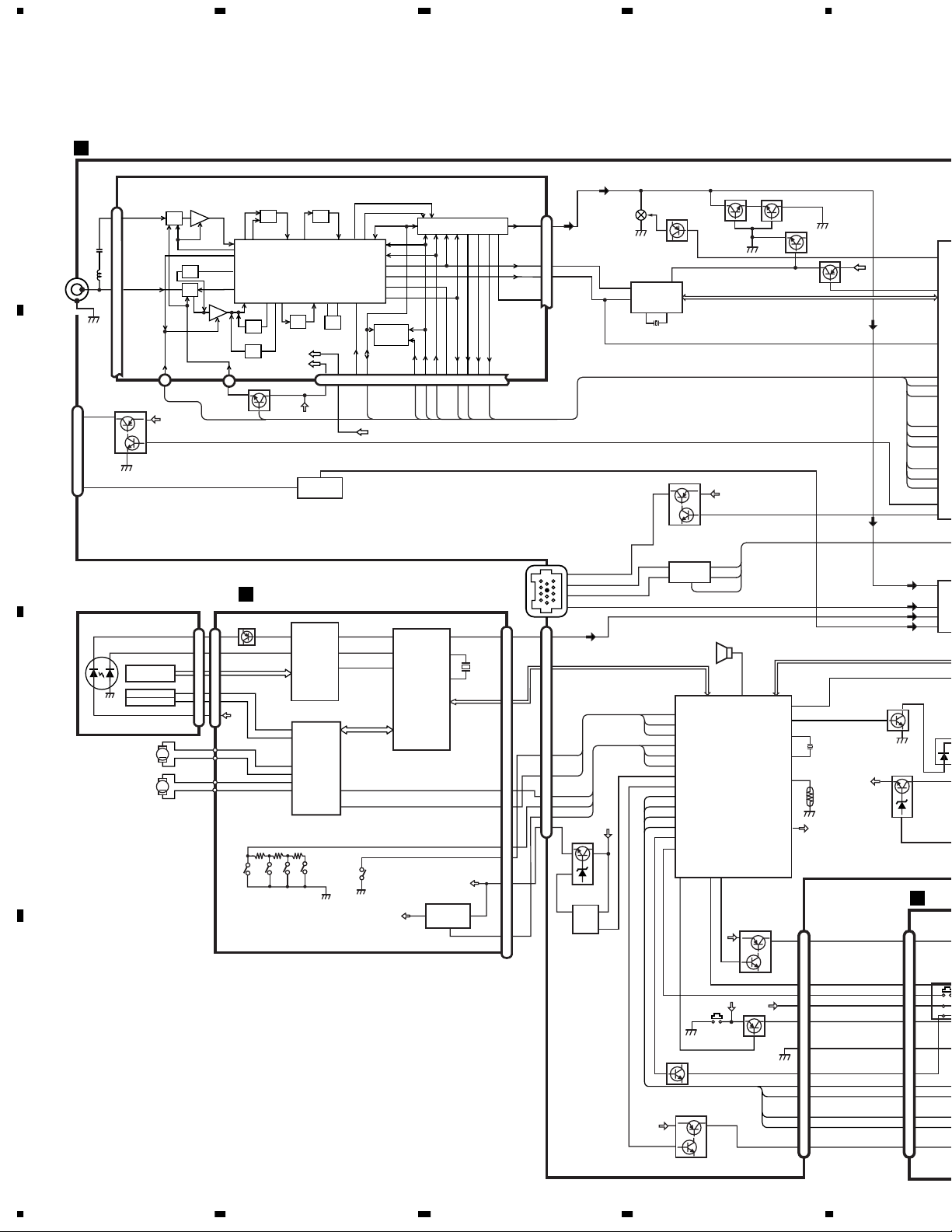
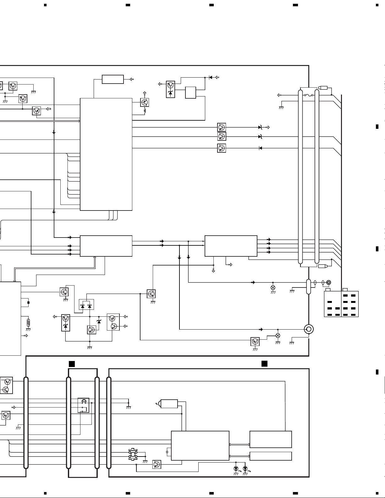
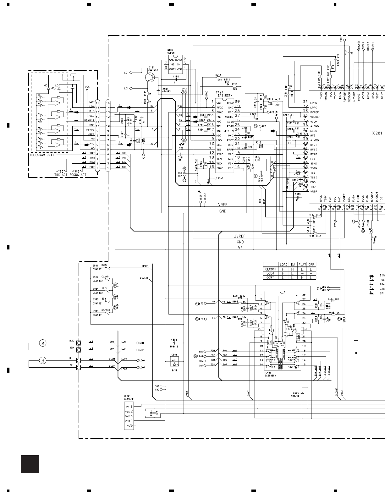
3. BLOCK DIAGRAM AND SCHEMATIC DIAGRAM
3.1 BLOCK DIAGRAM
TUNER AMP UNIT
A
B
C
D
A
FM/AM TUNER UNIT
AMANT
28
ANT
CN402
27
7
9
11
17
20
24
26
CN201
5
2
PICKUP UNIT(SERVICE)(P9)
LASER
DIODE
MONITOR
DIODE
LOAD/
10
1234
FMANT
WC
NC
DGND
NC
NC
FMLOCL
RFGND
Q215
Q216
HOLOGRAM
UNIT
FOCUS ACT.
TRACKING ACT.
SPINDLE
MOTOR
CARRIAGE
MOTOR
ATT
LOCH
23
VDD
M
M
AMRF
ANT ADJ
ATT
LD-
MD
FO+
TO+
LD+
FM/AM 1ST IF 10.7MHz
FMRF
IMG ADJ
RF ADJ
LOCL
25
LOCH
D
CN101
Q101
15
5
AC,BD
F,E
FOP
4
TOP
1
14
VDD
CLAMP
SENSE
T51 Q51 CF51
CF52 CF53
IC1
MIXER, IF AMP, DET.
CF202
AM 2ND IF
10.25MHz
450kHz
VDD
VCC
Q410
VCC
LOCL
1
2
IC 212
NJM2068MD
CONTROL UNIT
9
LDO
RFRPIN
8
MDI
RF-AMP
IC 101
TA2153FN
12
FOP
14
TOP
CD
DRIVER
16
SOP
15
SOM
17
LCOP
18
LCOM
IC 401
BA5996FM
12EJ
DISC
SENSE
SENSE
8EJ
SENSE
MPXREF 41kHz
AMDET
X901
22 19 12 15 16 8
10
FEO
TEO
LOEJ
MUTE
S901
HOME
IC 3
EEPROM
DI/DO
CREQ
14
PDIO
24
16
14
TD/FD
SD/MD
22
9
CE2CKCE1
VDD
38
43
46
RFI
FEI
TEI
SERVO
CONTROL,
DSP,
LPF, DAC
IC 201
TC9495F2
L_OUT
+5V REGULATOR
4
VDD
BA05SFP
DEH-P4400R/XN/EW
IC 2 FM MPX
SDBWSLFMSD
13 3
2
85
78
79
VD
IC 701
1
NL1
CN701
L-OUT
CONT
DSCSNS
HOME
2
CD5VON
STIND
1
LOEJ
Q420
20
8
COMP
LDET
L ch
6
21
18
NL2
4
CN701
8
BUS–
5
BUS+
1
BUS+L
7
14
16
11
10
17
1
2
CN501
6
Q510
Q511
B.U
1
5
14
10
11
17
16
VD
2
1
RDS
DECODER
IC 481
PM4009A
X481
Q416
IP-BUS DRIVER
B.U
Q413
1211
Q710
Q711
5
IC 710
6
HA12187FP
BUZZER
64
HOME
53
EJECT
63
CONT
54
LOEJ
79
DSCSNS
56
CD5VON
57
VDCONT
6
LCDPW
96
DPDT
95
KYDT
29
ROT0
25
ROT1
9
FLPILM
4
EJECTIN
Q752
1
2
8
IPPW
BZ610
ALARM
CONTROLLER
CSENS
SWVDD
23 20
77
S750
DETACH
SENSE SW
Q754
Q755
Q415
B.U
TX
RX
100
PEE
SYSTEM
IC 601(2/2)
PE5245A
ILMPW
B.U
VDD
Q751
Q753
Q414
Q411
MUTE
mute
TEMP
SYSPW
Q481
72
37
16
X1
X2
15
81
21
X610
TH601
SYSPW
VDD
Q362
mute
Q910
VCC
CN750
ILB+
7
CSENS
4
EJECT
8
FILM+
55
B.U
SW5V
10
Q750
99
FILM–
66
DPDT
11
KYDT
14
ROT1
12
ROT0
13
BL+B
2
7
4
8
10
11
14
12
13
2
42
88
32
38
39
50
51
74
97
98
99
71
41
44
42
40
B
CN1950
48
1
PA
EJEC
t
pc
SD
st
LO
LO
SL
PC
PD
PC
HF
AS
TU
BU
CD
IN1
Q91
S19
Page 11
A
B
R
5678
100
EE
TEM
OLLER
1(2/2)
245A
Q414
MUTE
mute
TEMP
SYSPW
RESET
1
IC 603
S-80834ANY
Q411
Q481
72
37
16
X1
X2
15
81
21
X610
TH601
SYSPW
VDD
32
38
39
50
51
74
97
98
99
71
41
44
42
40
Q362
mute
Q910
VCC
11
48
tmute
reset
42
88
1
SYSTEM
CONTROLLER
IC 601(1/2)
PE5245A
pce@
SD
st
LOCL
LOCH
SL
PCK
PDO
PCE1
HFPW
ASENBO
ELECTRONIC VOLUME/
SOURCE SELECTOR
TUN L
BUS+L
CD L
IN1L
Q918
86 85 24
IC 301
PML008A
MUTE
20
TXRXIPPW
Q911
Q912
2
adpw
AVREF
DALMON
bsens
asens
isens
Fout L
Rout L
SYSPW
VDD
Q913
VDD
1
VDD
Q610
22
83
10
93
92
8
6
Q909
5
B.U
Q914
Q915
Q917
CN901
BACK UP
B.U
B.U
GND
ACC
15
16
13
ILM
11
BACK UP
15
GND
16
ACC
13
ILM
11
10
11
Q361
B.U
14
FLIN
12
RLIN
22 4 25
VCC
IC 361
PAL007A
SYSPW
POWER AMP
RL–
RL+
FL–
FL+
B.REMSTBYMUTE
Q359
3
5 RL+
23 FL–
21 FL+
B.REM
Q341
Q351
RL–
CN331
CN351
7
5
8
6
12
1
2
Lch
5
8
6
12
FRONT
REAR/SW
RL+
FL–
FL+
B.REM
BACK UP
ILL
GND
B.REM
ACC
RR–
FR–
FL–
RL–
RR+
FR+
FL+
RL+
C
RL–
7
Q751
Q753
KEYBOARD UNIT
KEY MATRIX
7
C
D
LCD
11
8
PANEL UNIT
B
CN750
ILB+
7
CSENS
4
EJECT
8
FILM+
B.U
55
SW5V
10
Q750
99
FILM–
66
DPDT
11
KYDT
14
ROT1
12
ROT0
13
BL+B
2
CN1950
7
4
8
10
11
14
12
13
2
CN1951
EJECT SW
S1950
CN1901
IL+B
4
9
CSENS
3
10
µGND
6
7
SW5V
5
8
DPDT
10
3
KYDT
8
5
7
6
9
4
2
11
RDT1
RDT0
BL+B
S1922
REMOTE CONTROL
SENSOR
IC 1902
OPT IN
RS-140
X1901
Q1905
1
3
23 10
VDD
9
REMIN
DPDT
8
KYDT
X0
X1
DIMMER
7
LCD DRIVER
IC 1903
PD6294A
3
2
KEY DATA
LCD DATA
DEH-P4400R/XN/EW
56
Page 12
d
e
i
A-a
A-b
A-a
A-b
A-b
A-a
1234
3.2 OVERALL CONNECTION DIAGRAM(GUIDE PAGE)
Note: When ordering service parts, be sure to refer to " EXPLODED VIEWS AND PARTS LIST" or
"ELECTRICAL PARTS LIST".
A
A-a
A-a
A-b
A-b
Large size
SCH diagram
Guide page
FM(100%):-15.5dBs
AM(30%) :-26dBs
A-a
MIC, TEL
>
200mA
A-b
Detailed page
FM/AM TUNER UNIT
A-a
B
PE5245A
DSP-201M
PM4009A
SYSTEM CONTROLLER
DETACH SENSE SW
C
D
12
A B
EJECT
KEYBOARD UNIT
C
PANEL UNIT
B
CD:+4.1dBs
CONTROL UNIT
D
DEH-P4400R/XN/EW
1234
The > mark foun
the importance of
Therefore, when r
identical designat
Page 13

A
B
5678
" or
MIC, TEL
>
200mA
PE5245A
SYSTEM CONTROLLER
IP-BUS:+2.2dBs
CD: +4.1dBs
IP-BUS: +2.2dBs
AM(30%): -26dBs
FM(100%):-15.5dBs
FM(100%): +6.6dBs
AM(30%): -3.9dBs
CD:+10.2dBs
IP-BUS:+10.3dBs
A-b
TUNER AMP UNIT
A
600µH
472/16
CD:+9.4dBs
DETACH SENSE SW
The > mark found on some component parts indicates
the importance of the safety factor of the part.
Therefore, when replacing, be sure to use parts of
identical designation.
>
CEK1136
10A
For resistors and capacitors in the circuit diagrams, their resistance values or
capacitance values are expressed in codes:
Ex. *Resistors
Code Practical value
123 12k ohms
103 10k ohms
*Capacitors
Code Practical value
103 0.01uF
101/10 100uF/10V
FM(100%):+32.6dBs
AM(30%):+23.1dBs
IP-BUS:+36.3dBs
FUSE
BACK UP
ILL
B.REM
GND
ACC
CD:+36.2dBs
RR—
RR+
FR—
FR+
FL—
FL+
RL—
RL+
C
D
DEH-P4400R/XN/EW
56
A
13
7
8
Page 14
2
R
A-b
A
1234
1
SYSTEM CONTROLLE
A-b
A-a
MIC, TEL
B
200mA
>
PE5245A
C
D
14
A-a
PM4009A
DSP-201M
AM(30%) :-26dBs
FM(100%):-15.5dBs
FM/AM TUNER UNIT
DEH-P4400R/XN/EW
1234
Page 15
A
B
R
PM4009A
SYSTEM CONTROLLE
5678
Thethe
Theide
DETACH SENSE
2
EJECT
3
A-b
A-b
A-a
PANEL UNIT
C
KEYBOARD UNIT
B
C
DEH-P4400R/XN/EW
56
CD:+4.1dBs
D
D
CONTROL UNIT
B
A-a
15
7
8
Page 16
1234
A-b
A
B
A-a
TUNER AMP UNIT
A
CD:+9.4dBs
600µH
472/16
CD:+36.2dBs
IP-BUS:+36.3dBs
AM(30%):+23.1dBs
FM(100%):+32.6dBs
FUSE
>
CEK1136
10A
C
D
A-b
16
CD:+10.2dBs
IP-BUS:+10.3dBs
AM(30%): -3.9dBs
FM(100%): +6.6dBs
IP-BUS: +2.2dBs
CD: +4.1dBs
AM(30%): -26dBs
FM(100%):-15.5dBs
IP-BUS:+2.2dBs
1
A
DEH-P4400R/XN/EW
1234
M CONTROLLER
Page 17
A
B
600µH
5678
FL+
RL+
FR+
RR+
FL—
RL—
FR—
CD:+36.2dBs
IP-BUS:+36.3dBs
AM(30%):+23.1dBs
FM(100%):+32.6dBs
FUSE
CEK1136
10A
>
472/16
RR—
CC
B CK UP
B.REM
ILL
GND
A-b
A-a
For resistors and capacitors in the circuit diagrams, their resistance values or
capacitance values are expressed in codes:
Ex. *Resistors
Code Practical value
123 12k ohms
103 10k ohms
*Capacitors
Code Practical value
103 0.01uF
101/10 100uF/10V
C
M CONTROLLER
DETACH SENSE SW
DEH-P4400R/XN/EW
56
D
The > mark found on some component parts indicates
the importance of the safety factor of the part.
Therefore, when replacing, be sure to use parts of
identical designation.
3
A-b
17
7
8
Page 18

1234
3.3 KEYBOARD UNIT
A
B
PGM
C
S1901,S1902,
S1904,S1906,
S1907,S1909-S1919
CAW1627(P4400R),CAW1668(P4400RB)
CSG1107
CSG1133
Model
DEH-P4400R/XN/EW
DEH-P4400RB/XN/EW
Model
DEH-P4400R/XN/EW
DEH-P4400RB/XN/EW
D
C
18
1234
DEH-P4400R/XN/EW
Page 19
A
B
5678
KEYBOARD UNIT
C
PGM
CSG1111
CN1951
B
C
DEH-P4400R/XN/EW
56
D
C
19
7
8
Page 20
1234
5
S
L
O
A
E
J
r
o
s
o
o
3.4 CD MECHANISM MODULE
A
PICKUP UNIT(SERVICE)(P9)
RF AMP
CN101
SERVO CON
TC949
B
ACT/MOTOR DRIVER
SWITCHE
NOTE :
Symbol indicate
No differentiati
discrete resistor
Symbol indicate
No differentiati
discrete capacit
CONTRO
S901 : H
S902 : CL
S903 : DS
S904 : 12
S905 : 8E
The unde
C
SPINDLE
M1 CXB6007
LOADING/CARRIAGE
M2 CXB5903
D
5V REGULATOR
20
D
DEH-P4400R/XN/EW
1234
Page 21

A
B
5678
SERVO CONTROL/DSP/DAC/LPF
TC9495F2
CONTROL UNIT
D
R DRIVER
SWITCHES:
CONTROL UNIT
S901 : HOME SWITCH.....ON-OFF
S902 : CLAMP SWITCH....ON-OFF
S903 : DSCSNS SWITCH....ON-OFF
S904 : 12EJ SWITCH....ON-OFF
S905 : 8EJ SWITCH....ON-OFF
The underlined indicates the switch position.
NOTE :
Symbol indicates a resistor.
No differentiation is made between chip resistors and
discrete resistors.
Symbol indicates a capacitor.
No differentiation is made between chip capacitors and
discrete capacitors.
16.934MHz
Decimal points for resistor
and capacitor fixed values
are expressed as :
←
2.2 2R2
←
0.022 R022
C
DEH-P4400R/XN/EW
56
CN701
A
CN501
D
D
21
7
8
Page 22

1234
- Waveforms
1 CH1:DSCSNS 5V/div.
2 CH2:CLCONT 5V/div.
A
3 CH3:LOEJ 5V/div.
4 CH4:VD 10V/div.
When loading (12 cm CD)
500ms/div.
Note:1. The encircled numbers denote measuring pointes in the circuit diagram.
2. Reference voltage
VREF:2.1V
1 CH1:DSCSNS 5V/div.
2 CH2:CLCONT 5V/div.
3 CH3:LOEJ 5V/div.
500ms/div.
5 CH1:FD 500mV/div.
6 CH2:FOK 5V/div.
7 CH3:MD 5V/div.
500ms/div.
4 CH4:VD 10V/div.
When loading (8 cm CD)
When setting up "Source On"
Ref. :
GND
Mode :
Normal
5 CH1:FD 500mV/div.
6 CH2:FOK 5V/div.
7 CH3:MD 5V/div.
Magnified drawing for "time"
B
Ref. :
VREF
Mode :
Normal
8 CH1:FE 500mV/div.
5 CH2:FD 500mV/div.
0 CH3:TE 500mV/div.
! CH4:TD 500mV/div.
During "Play"
100ms/div.
1ms/div.
Ref. :
GND
Mode :
Normal
8 CH1:FE 500mV/div.
9 CH2:FOON 5V/div.
When setting up "Source On"
Ref. :
VREF
Mode :
Normal
@ CH1:BCK 2V/div.
During "Play"
500ms/div.
1µs/div.
Ref. :
VREF
Mode :
Normal
0 CH1:TE 500mV/div.
8 CH2:FE 500mV/div.
When setting up "Source On"
Ref. :
VREF
Mode :
Normal
# CH1:LRCK 2V/div.
$ CH2:DOUT 2V/div.
During "Play"
200ms/div.
10µs/div.
Ref. :
VREF
C
Mode :
Normal
7 CH1:MD 500mV/div.
During "Play"
Ref. :
VREF
Mode :
Normal
D
10µs/div.
Ref. :
VREF
Mode :
Normal
% CH1:RFO 500mV/div.
During "Play"
Ref. :
VREF
Mode :
Normal
0.5µs/div.
Ref. :
VREF
Mode :
Normal
% CH1:RFO 500mV/div.
0 CH2:TE 500mV/div.
During "Tracking Open"
Ref. :
VREF
Mode :
Test
2ms/div.
22
1234
DEH-P4400R/XN/EW
Page 23

A
B
5678
5 CH1:FD 1V/div.
^ CH2:FOP 2V/div.
With no disk inserted
During "Focus Close"
Ref. :
VREF
Mode :
Test
% CH1:RFO 1V/div.
0 CH2:TE 1V/div.
! CH3:TD 1V/div.
100 Track Jump
Ref. :
VREF
Mode :
Test
200ms/div.
5ms/div.
% CH1:RFO 1V/div.
0 CH2:TE 500mV/div.
500µs/div.
! CH3:TD 1V/div.
1 Track Jump
Ref. :
VREF
Mode :
Test
% CH1:RFO 2V/div.
& CH2:DFCT 5V/div.
5 CH3:FD 1V/div.
500µs/div.
! CH4:TD 2V/div.
When reproducing black dots (800µm)
Ref. :
VREF
Mode :
Normal
% CH1:RFO 1V/div.
0 CH2:TE 1V/div.
! CH3:TD 1V/div.
32 Track Jump
Ref. :
VREF
Mode :
Test
% CH1:RFO 1V/div.
0 CH2:TE 500mV/div.
& CH3:DFCT 5V/div.
During inside/outside search
Ref. :
VREF
Mode :
Normal
5ms/div.
200ms/div.
* CH1:TEY 500mV/div.
( CH2:SD 2V/div.
During inside/outside search
Ref. :
VREF
Mode :
Normal
) CH1:LOUT 2V/div.
⁄ CH2:ROUT 2V/div.
"Play" in 1kHz, 0dB
Ref. :
GND
Mode :
Normal
200ms/div.
200µs/div.
1 CH1:DSCSNS 5V/div.
2 CH2:CLCONT 5V/div.
3 CH3:LOEJ 5V/div.
When "Eject" (12 cm CD)
Ref. :
GND
Mode :
Normal
200ms/div.
1 CH1:DSCSNS 5V/div.
2 CH2:CLCONT 5V/div.
3 CH3:LOEJ 5V/div.
When "Eject" (8cm CD)
Ref. :
GND
Mode :
Normal
200ms/div.
C
DEH-P4400R/XN/EW
56
D
23
7
8
Page 24

1234
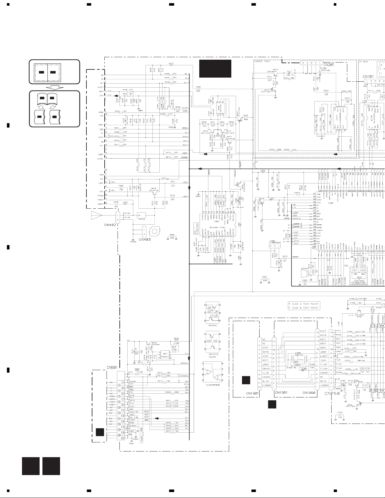
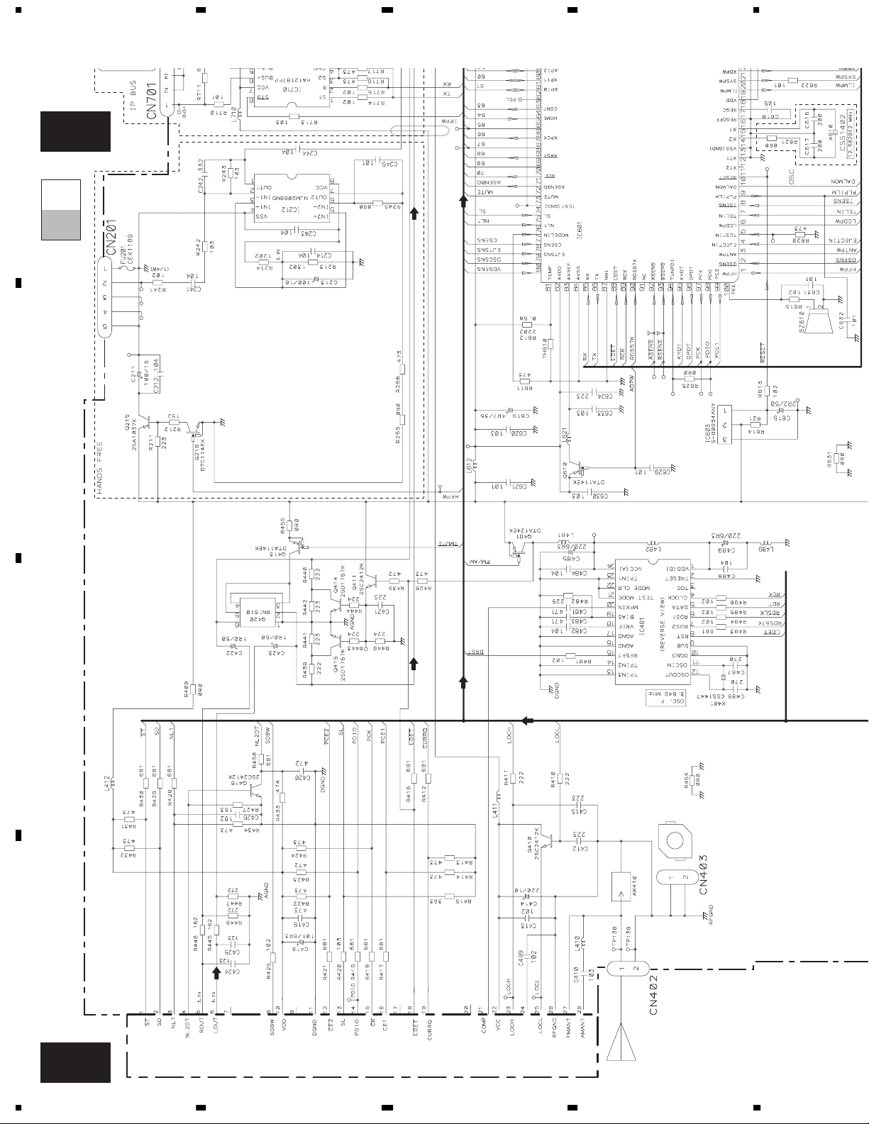
4. PCB CONNECTION DIAGRAM
4.1 TUNER AMP UNIT
NOTE FOR PCB DIAGRAMS
1.The parts mounted on this PCB
include all necessary parts for
A
B
several destination.
For further information for
respective destinations, be sure
to check with the schematic dia gram.
2.Viewpoint of PCB diagrams
Connector
P.C.Board
Capacitor
Chip Part
SIDE A
SIDE B
TUNER AMP UNIT
A
CORD ASSY
C
D
DETACH
SENSE SW
D
24
A
DEH-P4400R/XN/EW
1234
CN701
Page 25

A
B
5678
SIDE A
REAR OUTPUT
IP-BUS INPUT
ANTENNA
JACK
CORD ASSY
C
FM/AM TUNER UNIT
CN1950
B
FRONT
DEH-P4400R/XN/EW
56
D
A
25
7
8
Page 26

1234
TUNER AMP UNIT
A
A
B
C
D
A
26
1234
DEH-P4400R/XN/EW
Page 27

A
B
5678
SIDE B
C
DEH-P4400R/XN/EW
56
D
A
27
7
8
Page 28

1234
4.2 PANEL UNIT
PANEL UNIT
B
A
EJECT
B
SIDE A SIDE B
PANEL UNIT
B
C
A
CN750
C
CN1901
D
B
28
1234
DEH-P4400R/XN/EW
Page 29

A
B
5678
4.3 KEYBOARD UNIT
KEYBOARD UNIT
C
EQ
SOURCE
1
2
VOLUME
SIDE A SIDE B
PGM
DISPLAY
KEYBOARD UNIT
C
3
4
5
6
BAND
C
B
CN1951
FUNCTION
D
SFE
AUDIO
DEH-P4400R/XN/EW
56
C
29
7
8
Page 30

1234
4.4 CD MECHANISM MODULE
CONTROL UNIT
D
A
M2 LOADING/CARRIAGE MOTOR
M1 SPINDLE MOTOR
B
12EJ
DSCSNS
SIDE A
A
CN501
HOME
C
PICKUP UNIT(SERVICE)(P9)
D
30
D
DEH-P4400R/XN/EW
1234
Page 31

A
B
5678
CONTROL UNIT
D
SIDE B
8EJ
CLAMP
DEH-P4400R/XN/EW
56
C
D
D
31
7
8
Page 32

1234
5. ELECTRICAL PARTS LIST
NOTE:
• Parts whose parts numbers are omitted are subject to being not supplied.
• The part numbers shown below indicate chip components.
A
Chip Resistor
RS1/_S___J,RS1/__S___J
Chip Capacitor (except for CQS.....)
CKS....., CCS....., CSZS.....
cuit Symbol and No. Part NameParts No.
Circuit Symbol and No. Part NameParts No.
A
Unit Number:CWM8010
Unit Name:Tuner Amp Unit
MISCELLANEOUS
B
IC 212 IC NJM2068MD
IC 301 IC PML008A
IC 361 IC PAL007A
IC 481 IC PM4009A
IC 601 IC PE5245A
IC 603 IC S-80834ANY
IC 710 IC HA12187FP
Q 215 Transistor 2SA1037K
Q 216 Transistor DTC114EK
Q 341 Transistor IMH3A
Q 351 Transistor IMH3A
Q 359 Transistor DTA124EK
Q 361 Transistor DTC124EK
Q 362 Transistor DTC114EK
Q 410 Transistor 2SC2412K
Q 411 Transistor 2SC2412K
C
Q 413 Transistor DTA114EK
Q 414 Transistor 2SD1757K
Q 415 Transistor 2SD1757K
Q 416 Transistor 2SC2412K
Q 420 Transistor RN1610
Q 481 Transistor DTA124EK
Q 510 Transistor 2SD2396
Q 511 Transistor RN46A1
Q 610 Transistor DTA114EK
Q 710 Transistor 2SA1037K
Q 711 Transistor DTC114EK
Q 750 Transistor 2SA1037K
Q 751 Transistor 2SA1036K
Q 752 Transistor DTC114EK
Q 753 Transistor DTC114EK
Q 754 Transistor 2SA1037K
D
Q 755 Transistor DTC114EK
Q 909 Transistor RN46A1
Q 910 Transistor 2SD2396
Cir
Q 911 Transistor 2SB1243
Q 912 Transistor DTC114EK
Q 913 Transistor 2SD1760F5
Q 914 Transistor 2SC2412K
Q 915 Transistor 2SC2412K
Q 916 Transistor 2SA1037K
Q 917 Transistor 2SC2412K
Q 918 Transistor 2SC2412K
D 320 Diode DAN202U
D 361 Diode S5688G
D 362 Diode S5688G
D 510 Diode HZS9L(B1)
D 750 Diode 1SS270
D 751 Diode 1SS270
D 752 Diode DAP202U
D 753 Diode DAN202U
D 754 Diode DAP202K
D 755 Diode DAN202K
D 762 Diode DAN202U
D 763 Diode DAP202U
D 910 Diode HZS9L(B3)
D 911 Diode HZS6L(B2)
D 912 Diode S5688G
D 913 Diode HZS7L(C2)
D 914 Diode HZS7L(A1)
D 915 Diode 1SS270
D 916 Diode 1SS270
D 919 Diode S5688G
D 920 Diode S5688G
D 925 Diode 1SS270
D 926 Diode HZS9L(A2)
L 311 Ferri-Inductor LAU4R7K
L 361 Choke Coil 600µH CTH1221
L 410 Ferri-Inductor LAU4R7K
L 411 Ferri-Inductor LAU2R2K
L 412 Ferri-Inductor LAU2R2K
L 481 Inductor LAU100K
L 482 Ferri-Inductor LAU101K
L 489 Inductor CTF1346
L 612 Inductor LAU100K
L 621 Inductor CTF1346
L 710 Ferri-Inductor LAU2R2K
L 750 Ferri-Inductor LAU2R2K
L 910 Ferri-Inductor LAU2R2K
TH 610 Thermistor CCX1037
32
1234
DEH-P4400R/XN/EW
Page 33

A
B
5678
cuit Symbol and No. Part NameParts No.
Cir
X 481 Crystal Resonator 3.648MHzCSS1447
X 610 Radiator 12.58291MHz CSS1402
S 750 Switch(DETACH SENSE) CSN1039
FU 210 Fuse 200mA CEK1189
FM/AM Tuner Unit CWE1562
BZ 610 Buzzer CPV1050
AR 410 Arrester DSP-201M
RESISTORS
R 211 RS1/16S223J
R 212 RS1/16S152J
R 213 RN1/16SE1302D
R 214 RN1/16SE1002D
R 241 RD1/4PU102J
R 242 RS1/16S103J
R 243 RS1/16S103J
R 245 RS1/16S0R0J
R 255 RS1/16S0R0J
R 256 RS1/16S473J
R 311 RS1/16S101J
R 312 RS1/16S101J
R 313 RS1/16S101J
R 314 RS1/16S101J
R 327 RS1/16S222J
R 328 RS1/16S222J
R 341 RS1/16S223J
R 342 RS1/16S821J
R 343 RS1/16S821J
R 344 RS1/16S223J
R 351 RS1/16S821J
R 352 RS1/16S821J
R 353 RS1/16S223J
R 354 RS1/16S223J
R 361 RS1/16S103J
R 362 RS1/16S103J
R 363 RS1/16S331J
R 364 RS1/16S153J
R 365 RD1/4PU182J
R 409 RS1/16S0R0J
R 410 RS1/16S222J
R 411 RS1/16S222J
R 412 RS1/16S681J
R 413 RS1/16S473J
R 414 RS1/16S473J
R 415 RS1/16S393J
R 416 RS1/16S681J
R 417 RS1/16S681J
R 418 RS1/16S681J
R 419 RS1/16S681J
R 420 RS1/16S103J
R 421 RS1/16S681J
R 422 RS1/16S473J
R 423 RS1/16S472J
R 424 RS1/16S473J
R 425 RS1/16S102J
R 426 RS1/16S473J
R 427 RS1/16S153J
R 428 RS1/16S681J
R 429 RS1/16S681J
DEH-P4400R/XN/EW
56
cuit Symbol and No. Part NameParts No.
Cir
R 430 RS1/16S681J
R 431 RS1/16S473J
R 432 RS1/16S473J
R 433 RS1/16S474J
R 434 RS1/16S473J
R 435 RS1/16S472J
R 439 RS1/16S222J
R 440 RS1/16S222J
R 441 RS1/16S223J
R 442 RS1/16S223J
R 443 RS1/16S224J
R 444 RS1/16S224J
R 445 RS1/16S162J
R 446 RS1/16S162J
R 447 RS1/16S272J
R 448 RS1/16S272J
R 449 RS1/16S224J
R 450 RS1/16S681J
R 454 RS1/16S0R0J
R 455 RS1/16S0R0J
R 481 RS1/16S102J
R 482 RS1/16S225J
R 483 RS1/16S681J
R 484 RS1/16S102J
R 485 RS1/16S102J
R 486 RS1/16S102J
R 510 RD1/4PU221J
R 511 RD1/4PU221J
R 512 RS1/16S472J
R 513 RS1/16S222J
R 516 RS1/16S104J
R 517 RS1/16S222J
R 519 RS1/16S102J
R 520 RS1/16S0R0J
R 521 RS1/16S222J
R 523 RS1/16S0R0J
R 525 RS1/16S222J
R 526 RS1/16S222J
R 527 RS1/16S222J
R 528 RD1/4PU0R0J
R 529 RD1/4PU0R0J
R 530 RS1/16S0R0J
R 531 RS1/16S0R0J
R 532 RS1/16S0R0J
R 536 RS1/16S102J
R 537 RS1/16S104J
R 611 RS1/16S473J
R 612 RS1/16S2202F
R 613 RS1/16S102J
R 614 RS1/16S821J
R 615 RS1/16S102J
R 616 RS1/16S0R0J
R 620 RS1/16S473J
R 621 RS1/16S0R0J
R 622 RS1/16S101J
R 624 RS1/16S104J
R 625 RS1/16S0R0J
R 630 RAB4C102J
R 631 RS1/16S0R0J
R 710 RS1/16S101J
7
8
C
D
33
Page 34

1234
cuit Symbol and No. Part NameParts No.
Cir
R 711 RS1/16S620J
R 712 RS1/16S101J
R 713 RS1/16S103J
R 714 RS1/16S102J
R 715 RS1/16S102J
A
R 716 RS1/16S473J
R 717 RS1/16S473J
R 718 RS1/16S102J
R 719 RS1/16S102J
R 720 RS1/16S223J
R 721 RS1/16S223J
R 722 RS1/16S821J
R 723 RS1/16S821J
R 724 RS1/16S222J
R 725 RS1/16S223J
R 726 RS1/16S472J
R 750 RS1/16S104J
R 751 RS1/16S103J
R 752 RS1/16S153J
R 753 RS1/16S153J
R 754 RS1/16S222J
R 756 RS1/16S433J
B
R 757 RS1/16S473J
R 758 RS1/16S102J
R 759 RD1/4PU222J
R 760 RS1/16S102J
R 763 RS1/16S222J
R 764 RS1/16S131J
R 765 RS1PMF390J
R 766 RS1/10S270J
R 767 RS1/16S103J
R 768 RS1/16S152J
R 769 RS1/16S152J
R 771 RS1/16S473J
R 773 RD1/4PU222J
R 774 RS1/16S102J
R 775 RS1/16S102J
R 776 RS1/16S220J
C
R 777 RS1/16S0R0J
R 778 RS1/16S103J
R 779 RS1/16S472J
R 781 RS1/16S104J
R 782 RS1/16S131J
R 783 RS1/16S131J
R 784 RS1/10S392J
R 786 RS1/16S102J
R 787 RS1/10S472J
R 788 RS1/10S222J
R 789 RS1/10S222J
R 909 RD1/4PU0R0J
R 910 RS1/16S0R0J
R 911 RD1/4PU121J
R 912 RS1/16S102J
R 913 RD1/4PU102J
R 914 RS1/16S103J
D
R 915 RS1/16S222J
R 916 RS1/16S133J
R 917 RS1/16S104J
R 918 RS1/16S104J
R 919 RS1/16S223J
cuit Symbol and No. Part NameParts No.
Cir
R 920 RS1/16S473J
R 921 RS1/16S103J
R 922 RS1/16S473J
R 923 RD1/4PU102J
R 924 RS1/16S472J
R 925 RD1/4PU153J
R 926 RS1/16S472J
R 927 RS1/16S102J
R 928 RS1/16S473J
R 929 RS1/16S104J
R 930 RS1/16S103J
R 931 RS1/16S103J
R 932 RD1/4PU102J
R 933 RS1/16S473J
R 934 RS1/16S103J
R 935 RS1/16S223J
R 936 RD1/4PU152J
CAPACITORS
C 211 CEJA100M16
C 212 CKSRYB104K16
C 213 CEJA100M16
C 214 CKSRYB104K16
C 241 CKSRYB104K16
C 242 CKSRYB332K50
C 243 CKSRYB104K16
C 244 CKSRYB104K16
C 245 CCSRCH101J50
C 310 CKSRYB102K50
C 311 CEJA1R0M50
C 312 CEJA1R0M50
C 314 CKSRYB105K6R3
C 315 CKSRYB105K6R3
C 316 CKSRYB104K16
C 317 CKSRYB104K16
C 318 CKSRYB105K6R3
C 319 CKSRYB105K6R3
C 320 CKSRYB105K6R3
C 321 CKSRYB105K6R3
C 325 CKSRYB102K50
C 326 CEJA100M16
C 328 CKSRYB104K16
C 329 CEJA470M10
C 342 CEJA2R2M50
C 343 CEJA2R2M50
C 351 CEJA2R2M50
C 352 CEJA2R2M50
C 361 4700µF/16V CCH1367
C 362 CKSQYB104K16
C 363 CKSQYB474K16
C 364 CKSQYB474K16
C 365 CKSQYB474K16
C 366 CKSQYB474K16
C 367 CKSQYB474K16
C 368 CKSQYB474K16
C 369 CKSQYB474K16
C 370 CKSQYB474K16
C 371 CEJA330M10
C 373 CKSQYB225K10
34
1234
DEH-P4400R/XN/EW
Page 35

A
B
5678
cuit Symbol and No. Part NameParts No.
Cir
C 374 CKSQYB225K10
C 375 CEJA100M16
C 410 CKSQYB103K50
C 412 CKSRYB223K25
C 413 CKSRYB102K50
C 414 CEJA220M10
C 415 CKSRYB223K25
C 418 CEAL101M10
C 419 CKSRYB473K16
C 420 CKSRYB472K50
C 421 CKSRYB223K25
C 422 CEJA1R0M50
C 423 CEJA1R0M50
C 424 CKSRYB123K25
C 425 CKSRYB123K25
C 426 CKSRYB182K50
C 481 CCSRCH471J50
C 482 CKSRYB104K16
C 483 CKSRYB471K50
C 484 CKSRYB104K16
C 485 CEAL220M6R3
C 486 CCSRCH270J50
C 487 CCSRCH270J50
C 488 CKSRYB104K16
C 489 CEAL220M6R3
C 499 CKSRYB102K50
C 510 CKSRYB473K16
C 511 CKSRYB102K50
C 512 CEJA101M16
C 615 CEAL2R2M50
C 616 CCSRCH200J50
C 617 CCSRCH200J50
C 618 CKSRYB105K6R3
C 619 CEAL4R7M35
C 620 CKSRYB103K50
C 621 CCSRCH101J50
C 624 CKSRYB223K25
C 629 CCSRCH101J50
C 630 CKSRYB103K50
C 631 CCSRCH101J50
C 632 CCSRCH101J50
C 633 CKSRYB103K50
C 634 CKSRYB472K50
C 710 CKSRYB104K16
C 711 CKSRYB473K16
C 712 CEJA1R0M50
C 713 CEJA1R0M50
C 714 CEJA1R0M50
C 715 CEJA1R0M50
C 750 CKSRYB103K25
C 751 CKSQYB104K16
C 765 CKSQYB103K50
C 799 CKSQYB473K16
C 910 330µF/16V CCH1326
C 911 CKSRYB103K25
C 912 CEJA101M16
C 913 CEJA101M10
C 914 CKSRYB473K16
C 915 CKSRYB103K25
C 916 470µF/16V CCH1331
DEH-P4400R/XN/EW
56
cuit Symbol and No. Part NameParts No.
Cir
C 920 CKSRYB104K16
C 921 CKSQYB104K16
C
Unit Number:CWM8306(DEH-P4400R)
:CWM8307(DEH-P4400RB)
Unit Name:Keyboard Unit
MISCELLANEOUS
IC 1902 HIC RS-140
IC 1903 IC PD6294A
Q 1905 Transistor DTC114EK
D 1901 Diode MA152WK
D 1902 Diode MA152WA
D 1917 LED NSSW440-9159
D 1918 LED NSSW440-9159
D 1928 LED(DEH-P4400R) SML-310PT
D 1928 LED(DEH-P4400RB) SML-310VT
D 1930 LED(DEH-P4400R) SML-310PT
D 1930 LED(DEH-P4400RB) SML-310VT
D 1931 LED(DEH-P4400R) SML-310PT
D 1931 LED(DEH-P4400RB) SML-310VT
D 1932 LED(DEH-P4400R) SML-310PT
D 1932 LED(DEH-P4400RB) SML-310VT
D 1938 LED(DEH-P4400R) SML-310PT
D 1938 LED(DEH-P4400RB) SML-310VT
D 1939 LED(DEH-P4400R) SML-310PT
D 1939 LED(DEH-P4400RB) SML-310VT
D 1941 LED(DEH-P4400R) SML-310PT
D 1941 LED(DEH-P4400RB) SML-310VT
X 1901 Ceramic Resonator 5MHz CSS1547
S 1901 Switch(DEH-P4400R) CSG1107
S 1901 Switch(DEH-P4400RB) CSG1133
S 1902 Switch(DEH-P4400R) CSG1107
S 1902 Switch(DEH-P4400RB) CSG1133
S 1903 Push Switch CSG1111
S 1904 Switch(DEH-P4400R) CSG1107
S 1904 Switch(DEH-P4400RB) CSG1133
S 1906 Switch(DEH-P4400R) CSG1107
S 1906 Switch(DEH-P4400RB) CSG1133
S 1907 Switch(DEH-P4400R) CSG1107
S 1907 Switch(DEH-P4400RB) CSG1133
S 1908 Push Switch CSG1111
S 1909 Switch(DEH-P4400R) CSG1107
S 1909 Switch(DEH-P4400RB) CSG1133
S 1910 Switch(DEH-P4400R) CSG1107
S 1910 Switch(DEH-P4400RB) CSG1133
S 1911 Switch(DEH-P4400R) CSG1107
S 1911 Switch(DEH-P4400RB) CSG1133
S 1912 Switch(DEH-P4400R) CSG1107
S 1912 Switch(DEH-P4400RB) CSG1133
S 1913 Switch(DEH-P4400R) CSG1107
S 1913 Switch(DEH-P4400RB) CSG1133
S 1914 Switch(DEH-P4400R) CSG1107
7
35
8
C
D
Page 36

1234
cuit Symbol and No. Part NameParts No.
Cir
S 1914 Switch(DEH-P4400RB) CSG1133
S 1915 Switch(DEH-P4400R) CSG1107
S 1915 Switch(DEH-P4400RB) CSG1133
S 1916 Switch(DEH-P4400R) CSG1107
S 1916 Switch(DEH-P4400RB) CSG1133
A
S 1917 Switch(DEH-P4400R) CSG1107
S 1917 Switch(DEH-P4400RB) CSG1133
S 1918 Switch(DEH-P4400R) CSG1107
S 1918 Switch(DEH-P4400RB) CSG1133
S 1919 Switch(DEH-P4400R) CSG1107
S 1919 Switch(DEH-P4400RB) CSG1133
S 1922 Encoder CSD1059
LCD(DEH-P4400R) CAW1627
LCD(DEH-P4400RB) CAW1668
RESISTORS
R 1901 RS1/16S222J
R 1902 RS1/16S222J
R 1903 RS1/16S470J
R 1904 RS1/16S470J
R 1905 RS1/16S121J
R 1906 RS1/16S2R2J
B
R 1910 RS1/16S151J
R 1911 RS1/16S151J
R 1912 RS1/16S151J
R 1913 RS1/16S151J
R 1914 RS1/16S151J
R 1915 RS1/16S151J
R 1917 RS1/16S151J
R 1919 RS1/16S151J
R 1920 RS1/16S151J
R 1927 RS1/16S472J
R 1929 RS1/16S0R0J
R 1930 RS1/16S101J
R 1931 RS1/16S101J
R 1935 RS1/16S393J
R 1936 RS1/16S151J
R 1939 RS1/16S151J
C
R 1941 RS1/16S151J
R 1942 RS1/16S151J
R 1943 RS1/16S151J
R 1945 RS1/16S121J
R 1958 RS1/16S151J
R 1961 RS1/16S121J
R 1970 RS1/16S0R0J
R 1972 RS1/16S0R0J
R 1976 RS1/16S151J
CAPACITORS
C 1902 CKSRYB104K16
C 1903 CSZS100M6R3
C 1905 CKSRYB104K16
C 1906 CKSRYB104K16
C 1907 CKSRYB104K16
D
C 1923 CKSQYF104Z50
C 1930 CKSQYF104Z50
Unit Number:CWM7375
Unit Name:Panel Unit
D 1950 LED CL220PGC
S 1950 Push Switch(EJECT) CSG1112
R 1952 RS1/16S101J
R 1953 RS1/16S101J
Unit Number:CWX2481
Unit Name:Control Unit
MISCELLANEOUS
IC 101 IC TA2153FN
IC 201 IC TC9495F2
IC 401 IC BA5996FM
IC 701 IC BA05SFP
Q 101 Transistor 2SD1664
Q 102 Transistor UMD2N
L 201 Inductor CTF1546
L 202 Inductor CTF1546
X 301 Ceramic Resonator 16.934MHz CSS1525
S 901 Spring Switch(HOME) CSN1051
S 902 Spring Switch(CLAMP) CSN1052
S 903 Spring Switch(DSCSNS) CSN1051
S 904 Spring Switch(12EJ) CSN1052
S 905 Spring Switch(8EJ) CSN1051
RESISTORS
R 101 RS1/16S222J
R 102 RS1/8S120J
R 103 RS1/8S100J
R 201 RS1/16S513J
R 202 RS1/16S513J
R 203 RS1/16S823J
R 204 RS1/16S823J
R 206 RS1/16S823J
R 208 RS1/16S124J
R 209 RS1/16S183J
R 210 RS1/16S153J
R 211 RS1/16S103J
R 212 RS1/16S103J
R 213 RS1/16S124J
R 215 RS1/16S0R0J
R 216 RS1/16S471J
R 301 RS1/16S333J
R 302 RS1/16S332J
R 303 RS1/16S332J
R 304 RS1/16S514J
cuit Symbol and No. Part NameParts No.
Cir
B
D
36
1234
DEH-P4400R/XN/EW
Page 37

A
B
5678
cuit Symbol and No. Part NameParts No.
Cir
R 306 RS1/16S102J
R 307 RS1/16S102J
R 312 RS1/16S103J
R 313 RS1/16S473J
R 315 RS1/16S334J
R 321 RS1/16S331J
R 322 RS1/16S0R0J
R 323 RS1/16S332J
R 401 RS1/16S684J
R 402 RS1/16S103J
R 403 RS1/16S103J
R 404 RS1/16S183J
R 405 RS1/16S123J
R 407 RS1/16S622J
R 408 RS1/16S622J
R 409 RS1/16S113J
R 410 RS1/16S752J
R 701 RS1/16S102J
R 702 RS1/16S221J
R 703 RS1/16S221J
R 704 RS1/16S221J
R 705 RS1/16S221J
R 706 RS1/16S221J
R 707 RS1/16S221J
R 708 RS1/16S102J
R 709 RS1/16S102J
R 710 RS1/16S102J
R 901 RS1/16S104J
R 902 RS1/16S473J
R 903 RS1/16S273J
CAPACITORS
C 101 CEV470M6R3
C 102 CKSRYB102K50
C 103 CKSRYB104K16
C 104 CKSRYB224K16
C 105 CEV470M6R3
C 106 CKSRYB104K16
C 107 CKSRYB105K6R3
C 201 CKSRYB104K16
C 202 CCSRCH560J50
C 204 CKSRYB224K16
C 205 CKSRYB224K16
C 206 CKSRYB273K25
C 207 CKSRYB273K25
C 208 CKSRYB104K16
C 209 CKSRYB104K16
C 210 CCSRCK2R0C50
C 211 CCSRCH220J50
C 301 CKSRYB153K25
C 302 CKSRYB104K16
C 303 CKSRYB103K50
C 304 CKSRYB103K50
C 305 CKSRYB104K16
C 306 CKSRYB104K16
C 307 CKSRYB333K16
C 308 CKSRYB104K16
Cir
cuit Symbol and No. Part NameParts No.
C 309 CKSRYB473K16
C 310 CKSRYB473K16
C 311 CKSRYB104K16
C 312 CKSRYB104K16
C 315 CEV220M6R3
C 317 CKSRYB104K16
C 318 CKSRYB104K16
C 319 CKSRYB104K16
C 320 CCSRCH470J50
C 325 CKSRYB471K50
C 328 CKSRYB472K50
C 329 CKSRYB104K16
C 330 CKSRYB104K16
C 331 CKSRYB104K16
C 401 CKSRYB221K50
C 402 CKSRYB221K50
C 403 CKSRYB153K25
C 404 CKSRYB103K50
C 405 CEV101M10
C 702 CKSRYB104K16
C 703 CKSRYB104K16
C 801 10µF/10V CCH1349
C 802 CEV101M10
C 803 CKSRYB224K16
Miscellaneous Parts List
Pickup Unit(Service)(P9) CXX1480
M 1 Motor Unit(SPINDLE) CXB6007
M2 Motor Unit(LOADING/CARRIAGE) CXB5903
C
D
DEH-P4400R/XN/EW
56
37
7
8
Page 38

1234
6. ADJUSTMENT
6.1 CD ADJUSTMENT
1) Precautions
• This unit uses a single power supply (+5V) for the reg-
A
B
ulator. The signal reference potential, therefore, is
connected to VREF(approx. 2.1V) instead of GND.
If VREF and GND are connected to each other by mistake during adjustments, not only will it be impossible to measure the potential correctly, but the servo
will malfunction and a severe shock will be applied to
the pick-up. To avoid this, take special note of the following.
Do not connect the negative probe of the measuring
equipment to VREF and GND together. It is especially
important not to connect the channel 1 negative
probe of the oscilloscope to VREF with the channel 2
negative probe connected to GND.
Since the frame of the measuring instrument is usually at the same potential as the negative probe, change
the frame of the measuring instrument to floating status.
If by accident VREF comes in contact with GND,
immediately switch the regulator or power OFF.
• Always make sure the regulator is OFF when connecting and disconnecting the various filters and wiring
required for measurements.
• Before proceeding to further adjustments and measurements after switching regulator ON, let the player
run for about one minute to allow the circuits to stabilize.
2) Test Mode
This mode is used for adjusting the CD mechanism
module of the device.
• Test mode starting procedure
Reset while pressing the 4 and 6 keys together.
• Test mode cancellation
Switch ACC, back-up OFF.
• After pressing the EJECT key, do not press any other
key until the disk is completely ejected.
• If the ] or [ key is pressed while focus search is in
progress, immediately turn the power off (otherwise
the actuator may be damaged due to adhesion of the
lenses).
• Jump operation of TRs other than 100TR continues
after releasing the key. CRG move and 100TR jump
operations are brought into the “Tracking close” status when the key is released.
• Powering Off/On resets the jump mode to “Single
TR(91)”, the RF AMP gain setting to 0 dB, and the
automatic adjustment value to the initial value.
• Since the protective systems in the unit's software are
rendered inoperative in test mode, be very careful to
avoid mechanical and /or electrical shocks to the system when making adjustment.
• The RFI and RFO signals are easy to oscillate because
C
D
of a wide band. When observing them, insert a resistor of about 1 kΩ to the series.
• This equipment will not guarantee the load ejection
operation when the mechanical unit is turned upside
down. In particular, if the ejection operation is incorrectly performed and recover
ery is enabled by resetting a product or turning ACC
off to on.
y is disabled, the recov-
38
1234
DEH-P4400R/XN/EW
Page 39

A
B
*1)
+12dB
TRK12 MIN12 SEC
12
TYP
TRK MIN SEC
*2) S. curve check setting
TRK01 MIN01 SEC
01
Focus Close setting
TRK00 MIN00 SEC
00
or
TRK99 MIN99 SEC
99
*8) CRG motor voltage = 2 [V]
*3)
T.Offset
Display
Switch to the order of the original display
F.Offset
Display
*7)
F.AGC
Gain
RF AGC
Gain
TRK/MIN/SEC
T.AGC
Gain
*5
Single TR
TRK
91
MIN
91
SEC
91
or
TRK
81
MIN
81
SEC
81
32TR
TRK
92
MIN
92
SEC
92
or
TRK
82
MIN
82
SEC
82
100TR
TRK
93
MIN
93
SEC
93
or
TRK
83
MIN
83
SEC
83
CRG Move
TRK
94
MIN
94
SEC
94
or
TRK
84
MIN
84
SEC
84
*4) 1TR/32TR/100TR
*6) Only at the time of CRG move or 100TR jump
[BAND]
Power On
(T. offset is adjusted)
TRK
00
MIN
00
SEC
00
[CD] or [SOURCE]
Source On
TRK MIN
[4]+[6]+Reset
Test Mode In
[3]
Power On
(T. offset is not adjusted)
TRK
99
MIN
99
SEC
99
[2]
RF AMP
Gain switching
*1
TRK
GG
MIN
GG
SEC
GG
[BAND]
Power Off
TRK MIN SEC
[BAND]
Power Off
TRK MIN SEC
[BAND]
Power Off
TRK MIN SEC
[BAND]
Power Off
TRK MIN SEC
[3]
Focus Close /
S. curve check
TRK
91
MIN
91
SEC
91
[6]
Focus Mode switching
*2
TRK
0x
MIN
0x
SEC
0x
[1]
Tracking Servo
Close
TRK
00
MIN
00
SEC
00
or
TRK
99
MIN
99
SEC
99
[[]
CRG-
*8
TRK
00
MIN
00
SEC
00
or
TRK
99
MIN
99
SEC
99
[]]
CRG+
*8
TRK
00
MIN
00
SEC
00
or
TRK
99
MIN
99
SEC
99
[6]
New Test Mode
[2]
Automatic adjustment value
display switching
*3
TRK
??
MIN
??
SEC
??
[1]
T.CLS and F,T AGC
and RF AGC and
Applicable servomechanism
TRK
xx
MIN
xx
SEC
xx
[6]
T.Close and
Applicable servomechanism
TRK
xx
MIN
xx
SEC
xx
[3]
RF AGC /
RF AGC coefficient display
TRK
??
MIN
??
SEC
??
[]]
CRG+
TRK
8x
MIN
8x
SEC
8x
or
TRK
9x
MIN
9x
SEC
9x
[[]
CRG-
TRK
8x
MIN
8x
SEC
8x
or
TRK
9x
MIN
9x
SEC
9x
[2]
T.Balance adjustment /
T.Balance coefficient display
TRK
??
MIN
??
SEC
??
[1]
F,T,RF AGC /
F.Bias display switching
*7
TRK
??
MIN
??
SEC
??
[3]
F,T AGC,F.Bias
and RF AGC
TRK
xx
MIN
xx
SEC
xx
[6]
CRG/TR jump value
*5
switching
TRK
xx
MIN
xx
SEC
xx
[]]
CRG+/TR Jump+
*4
TRK
xx
MIN
xx
SEC
xx
[[]
CRG-/TR Jump-
*4
TRK
xx
MIN
xx
SEC
xx
[2]
Tracking Open
TRK
8x
MIN
8x
SEC
8x
or
TRK
9x
MIN
9x
SEC
9x
[2]
Tracking Open
TRK
8x
MIN
8x
SEC
8x
or
TRK
9x
MIN
9x
SEC
9x
F. EQ measurement setting
TRK02 MIN02 SEC
02
[Key]
[BAND]
[]]
[[]
[1]
[2]
[3]
[6]
-
-
Power On/Off
CRG +/TR Jump+
(Direction of the external surface)
CRG -/TR Jump(Direction of the internal surface)
T.CLS and AGC and Applicable servomechanism/
AGC,AGC display switching
RF Gain switching/Offset adjustment display/
T.Balance adjustment/T.OPN
F.CLS,S.Curve/Rough Servo and RF AGC/
F,T,RF AGC
SPDL 1X/2X switching
(Double-speed compatibility only)
Error rate measurement
F.Mode switching/T.CLS/CRG,TR
Jump switching
Test Mode New Test Mode
Operation
Error occurrence time/
cause display switching
TRK+/FF
TRK-/REV
SCAN
MODE
(ITP)
-
-
Auto/Manual switching
F.Bias
[KEY]
Contents
Display
- Flow Chart
5678
56
DEH-P4400R/XN/EW
7
C
D
39
8
Page 40

1234
6.2 CHECKING THE GRATING AFTER CHANGING THE PICKUP UNIT
A
• Note :
The grating angle of the PU unit cannot be adjusted after the PU unit is changed. The PU unit in the CD mecha-
nism module is adjusted on the production line to match the CD mechanism module and is thus the best adjusted
PU unit for the CD mechanism module. Changing the PU unit is thus best considered as a last resort. However, if
the PU unit must be changed, the grating should be checked using the procedure below.
• Purpose :
To check that the grating is within an acceptable range when the PU unit is changed.
• Symptoms of Mal-adjustment :
If the grating is off by a large amount symptoms such as being unable to close tracking, being unable to perform
track search operations, or taking a long time for track searching.
• Method :
• Measuring Equipment • Oscilloscope, Two L.P.F.
• Measuring Points • E, F, VREF
• Disc • ABEX TCD-784
• Mode • TEST MODE
B
CONTROL UNIT
L.P.F.
E
100kΩ
VREF
F
VREF
VREF
E
F
C
390pF
100kΩ
390pF
L.P.F.
Xch Ych
Oscilloscope
• Checking Procedure
1. In test mode, load the disc and switch the 5V regulator on.
2. Using the ] and [ buttons, move the PU unit to the innermost track.
3. Press key 3 to close focus, the display should read "91". Press key 2 to implement the tracking balance adjust-
ment the display should now read "81". Press key 3. The display will change, returning to "81" on the fourth
press.
4. As shown in the diagram above, monitor the LPF outputs using the oscilloscope and check that the phase differ-
ence is within 75° . Refer to the photographs supplied to determine the phase angle.
5. If the phase difference is determined to be greater than 75° try changing the PU unit to see if there is any
improvement. If, after trying this a number of times, the grating angle does not become less than 75° then the
mechanism should be judged to be at fault.
• Note
Because of eccentricity in the disc and a slight misalignment of the clamping center the grating wavefor
seen to "wobble" ( the phase difference changes as the disc rotates). The angle specified above indicates the average angle.
m may be
D
• Hint
Reloading the disc changes the clamp position and may decrease the "wobble".
40
1234
DEH-P4400R/XN/EW
Page 41

A
B
5678
Grating waveform
0°
45°
Ech → Xch 20mV/div, AC
Fch → Ych 20mV/div, AC
30°
60°
75°
90°
DEH-P4400R/XN/EW
56
C
D
41
7
8
Page 42

1234
6.3 TEST MODE
- Error Messages
If a CD is not operative or stopped during operation due to an error, the error mode is turned on and cause(s) of the
A
B
C
error is indicated with a corresponding number. This arrangement is intended at reducing nonsense calls from the
users and also for facilitating trouble analysis and repair work in servicing.
(1) Basic Indication Method
1) When SERRORM is selected for the CSMOD (CD mode area for the system), error codes are written to DMIN (minutes display area) and DSEC (seconds display area). The same data is written to DMIN and DSEC. DTNO r
in blank as before.
2) Head unit display examples
Depending on display capability of LCD used, display will vary as shown below. xx contains the error number.
8-digit display 6-digit display 4-digit display
ERROR–xx ERR–xx E–xx
(2) Error Code List
Code Class Displayed error code Description of the code and potential cause(s)
10 Electricity Carriage Home NG CRG can't be moved to inner diameter.
SERVO LSI Com- CRG can't be moved from inner diameter.
munication Error → Failure on home switch or CRG move mechanism.
Communication error between microcomputer and SERVO LSI.
11 Electricity Focus Servo NG Focusing not available.
→ Stains on rear side of disc or excessive vibrations on REWRITABLE.
12 Electricity Spindle Lock NG Spindle not locked. Sub-code is strange (not readable).
Subcode NG → Failure on spindle, stains or damages on disc, or excessive vibrations.
A disc not containing CD-R data is found.
Turned over disc are found, though rarely.
CD signal error.
17 Electricity Setup NG AGC protection doesn't work. Focus can be easily lost.
→ Damages or stains on disc, or excessive vibrations on REWRITABLE.
30 Electricity Search Time Out Failed to reach target address.
→ CRG tracking error or damages on disc.
44 Electricity ALL Skip Skip setting for all track.
(CD-R/RW)
50
Mechanism
CD On Mech Error Mechanical error during CD ON.
→ Defective loading motor, mechanical lock and mechanical sensor.
A0 System Power Supply NG Power (VD) is ground faulted.
→ Failure on SW transistor or power supply (failure on connector).
Remarks: Mechanical errors are not displayed (because a CD is turned off in these errors).
Unreadable TOC does not constitute an error. An intended operation continues in this case.
Upper digits of an error code are subdivided as shown below:
1x: Setup relevant errors, 3x: Search relevant errors, Ax: Other errors.
emains
D
42
1234
DEH-P4400R/XN/EW
Page 43

A
B
5678
- New Test Mode
S-CD plays the same way as before.
If an error such as off focus, spindle unlocking, unreadable sub-code, or sound skipping occurs after setup, its
cause and time occurred (in absolute time) are displayed.
During setup, operational status of the control software is displayed.
These displays and functions are prepared for enhancing aging in the servicing and efficiency of trouble analysis.
(1) Shifting to the New Test Mode
1 Turn on the current test mode by starting the reset from the key.
2 Select S-CD for the source through the specified procedure including use of the [SOURCE] key, and inser
disc. Then, press the [Jump Mode Selector] key while maintaining the regulator turned off.
3 After the above operations, the new test mode remains on irrespective of whether the S-CD is turned on or off.
You can reset the new test mode by turning on the reset start.
(2) Key Correspondence
Key Test mode New test mode
Regulator Off Regulator On In-play Error Production
BAND To regulator on To regulator off – Time/Err.No. switching
] – FWD-Kick FF/TR+ –
[ – REV-Kick REV/TR- –
1 – Tracking Close Scan –
2 – Tracking Open Mode –
3 – Focus Close ––
–– Focus Open ––
–– Jump Of
f ––
6 To new test mode
Jump mode switching Auto/Manu –
Note: Eject and CD on/off is perfor
med in the same procedure as that for the normal mode.
(3) Cause of Error and Er
ror Code
Code Class Contents
Description and cause
40 Electricity Of
f focus detected. FOK goes low.
→ Damages/stains on disc, vibrations or failur
e on servo.
41 Electricity Spindle unlocked. LOCK = Low continued for 150 msec.
→ Damages/stains on disc, vibrations or failure on servo.
42 Electricity Sub-code unreadable. Sub-code was unreadable for 500 msec.
→ Damages/stains on disc, vibrations or failure on servo.
43 Electricity Sound skipping detected. Last address memory function was activated.
→ Damages/stains on disc, vibrations or failure on servo.
Note: Mechanical errors during aging are not displayed.
ting the
56
DEH-P4400R/XN/EW
7
C
D
43
8
Page 44

1234
(4) Display of Operational Status during Setup
Status No. Contents Protective action
21 Focus search start Focus search timeout.
22 Focus search 2 Focus search timeout.
23 Focus search 3 Focus search timeout.
A
24 Focus search 4 Focus search timeout.
25 Focus search(Setup protection) Focus slips off.
26 Focus search(Fast recovery) Focus slips off.
27 RF detection Focus slips off.
28 Spindle rough servocontrol Focus slips off.
29 Tracking balance adjustment start Focus slips off.
30 Tracking balance adjustment 2 Focus slips off.
31 Tracking balance adjustment 3 Focus slips off.
32
Tracking close start(Spindle stationary servocontrol setting)
Focus slips off.
33 Tracking close 2 Focus slips off.
34 Tracking close 3 Focus slips off.
35 Focus/Tracking AGC start Focus slips off.
36 Focus/Tracking AGC 2 Focus slips off.
37 Focus/Tracking AGC 3 Focus slips off.
38 Focus/Tracking AGC 4 Focus slips off.
39 Focus/Tracking AGC 5 Focus slips off.
B
40 Focus/Tracking AGC 6 Focus slips off.
41 Focus/Tracking AGC 7 Focus slips off.
42 Focus/Tracking AGC 8 Focus slips off.
43 FE bias start Focus slips off.
44 FE bias 2 Focus slips off.
45 RF AGC start Focus slips off.
46 RF AGC 2 Focus slips off.
47 Lock check start Focus slips off.
48 Lock is being checked Focus slips off.
49 Subcode check start Focus slips off, spindle lock is not performed.
50 Subcode is being checked Focus slips off, no subcode can be read.
C
D
44
1234
DEH-P4400R/XN/EW
Page 45

A
B
5678
(5) Display Examples
1) During Setup
8-digit display, 6-digit display 4-digit display(Auto setting) 4-digit display(Manual setting)
TNO. Min Sec TNO. Min Sec
11 11' 11" 11 11' 11"
2) During Operation (TOC read, TRK search, Play, FF and REV)
The same as in the normal mode.
3) When a Protection Error Occurred
(A) Error display ((A)←→(B), (C) : BAND key)
8-digit display 6-digit display 4-digit display
ERROR-xx ERR-xx E-xx
(B) Error occurrence timing display in track no. ((B)←→(C) : Auto/Manual key)
8-digit display, 6-digit display 4-digit display(Auto setting)
TNO. Min Sec TNO.
10 40' 05" 10
(C) Error occurrence timing display in absolute time. ((B)←→(C) : Auto/Manual key)
8-digit display, 6-digit display 4-digit display(Manual setting)
TNO. Min Sec Min Sec
10 40' 05" 40' 05"
C
DEH-P4400R/XN/EW
56
D
45
7
8
Page 46

1234
7. GENERAL INFORMATION
7.1 DIAGNOSIS
7.1.1 DISASSEMBLY
-
Removing the Case (not shown)
A
1. Remove the Case.
- Removing the CD Mechanism Module (Fig.1)
Remove the four screws.
Disconnect the connector and then remove the CD
Mechanism Module.
Removing the Grille Panel Assy (Fig.1)
-
CD Mechanism Module
Remove the two screws and then r
Grille Panel Assy.
B
- Removing the Tuner Amp Unit (Fig.2)
Remove the two screws.
Straight the tabs at three locations indicated.
Remove the screw.
C
Remove the three screws and then remove
the Tuner Amp Unit.
emove the
Grille Panel Assy
Fig.1
*) Tuner Amp Unit is different partially from this
photo.
D
46
1234
Tuner Amp Unit
Fig.2
DEH-P4400R/XN/EW
Page 47

A
B
5678
- How to hold the Mechanical Unit
1.Hold the top and bottom frame.
2.Do not squeeze top frame's front portion too tight,
because it is fragile.
- How to remove the Top and Bottom Frame
1.When the disk is "clamp" state, unlock Spring A (6
pieces) and Spring B (2 pieces), and unscrew screws
(4 pieces).
2.Unlock each 1 of pawl at the both side of the frame,
then remove the top frame.
3.Remove the Carriage Mechanical part in such way
that; you remove the mechanical part from 3 pieces
of Damper while slowly pulling up the part.
4.Now, the top frame has been removed, and under
this state, fix the genuine Connector again, and eject
the disk.
(Caution)
When you reassemble the Carriage Mechanical part,
apply a bit of alcohol to Dampers.
- How to remove the Guide Arm Assy
1.Unlock the spring (1 piece) at the right side of the
assembly.
2.Unscrew screws (2 pieces), then remove the Screw
Gear Bracket.
3.Shift the Guide Arm Assy to the left and slowly rotate
it to the upper direction.
4.When the Guide Arm Assy rotates approximately 45
degree, shift the Assy to the right side dir
ection and
remove it.
Top Frame
Bottom Frame
Damper
Screw Gear Bracket
Guide Arm
Assy
Carriage
Mechanical
Par
t
Do not squeeze.
C
56
DEH-P4400R/XN/EW
7
D
47
8
Page 48

1234
- How to remove the Control Unit
1.Give jumper-solder treatment to the Flexible Wire of
the Pickup unit, then remove the wire from the
Connector.
A
2.Remove all 4 points of solder-treatment on the Lead
Wire. Also, unscrew the screw(1 piece).
3.Then, Remove the Control unit.
(Caution)
Be careful not to damage SW when you reassemble
the Control Unit into the device.
- How to remove the Loading Arm Assy
1.Unlock the spring (1 piece) and remove the E ring (1
B
piece) of the Fulcrum Shaft.
2.Shift the arm to the left side direction and unlock pins
(2 pieces).
Jumper-Solder
Control Unit
Solder
C
- How to remove the Pickup Unit
1.Unscrew 2 pieces of screws, then remove the Pulley
Cover.
2.Remove the Feed Screw unit from the pawl of the
Feed Screw Guide (The pawl is located inside the
guide).
3.Remove the belt from the Pulley, then remove the
Pickup unit.
(Caution)
Make sure not to stain the belt with gr
fix the belt.
D
ease when you
Loading Arm Assy
Pulley Cover
GEM1035
ease Application
Gr
Grease Application
GEM1035
Pickup Unit
UD321BR
Gr
ease Application
Belt
Feed Screw Guide
48
1234
DEH-P4400R/XN/EW
Page 49

A
B
5678
111098
765
4321
RCA
BUSH
H/F
BUSH
15
16
10
2
51
REAR OUTPUT
ANTENNA JACK
FUSE 10A
1. BUS+
2. GND
3. GND
4. NC
5. BUS-
6. GND
7. BUS L+ INPUT
8. ASENB
9. BUS R+ INPUT
10. BUS R- INPUT
11. BUS L- INPUT
FRONT
OUTPUT
TEL
1. GND
2. B.UP
3. ACC
4. NC
5. ILM
6. B.REM
7.TELMUTE
8. NC
9. RL-
10. FL-
11. RL+
12. FL+
13. RR-
14. FR-
15. RR+
16. FR+
7.1.2 CONNECTOR FUNCTION DESCRIPTION
DEH-P4400R/XN/EW
56
C
D
49
7
8
Page 50

1234
7.2 PARTS
7.2.1 IC
PAL007A
A
Protector;
TAB
P-GND2
OUT2-
STBY
OUT2+
VCC
OUT1-
P-GND1
OUT1+
B
SVR
IN1
IN2
S-GND
IN4
IN3
AC-GND
OUT3+
P-GND3
OUT3-
VCC
OUT4+
C
MUTE
OUT4-
P-GND4
SWITCH
1
2
3
4
5
6
7
8
9
10
11
12
13
14
15
16
17
18
19
20
21
22
23
24
25
Over voltage
Protector;
Short circuit
Protector;
Over current limit
Stand-by
Circuit
Offset
Detection
Offset
Detection
Offset
Detection
Offset
Detection
stby
amp_vcc
+
-
+
+
-
+
+
-
+
+
-
+
sw_vcc
amp_vcc
sw_vcc
Protector;
Thermal
Reference
Mute circuit
D
50
DEH-P4400R/XN/EW
1234
Page 51

A
B
5678
DGND
CLK
Vref
NC
MUTE
STB
DATA
IN4 -_R
IN4+_R
IN3_R
IN1_R
IN2_R
Vcc
IN1_L
IN2_L
IN3_L
IN4+_L
IN4 -_L
12
11
10
9
8
7
6
5
4
3
2
1
2019181716
15
1413
30
29
28
27
26
25
24
23
2221
40 39 38 37 36 35 34
33
32
31
44 43 42 41
Tone_out_RL
SV_in_RL
SV_in_FL
Tone_out_FL
Front_out_L
Rear_out_L
NC
NC
NC
NC
PV_in_R
PV_in_L
Sel_out_R
AGND_L
NC
NC
NC
NC
Tone_out_FR
AGND_R
SV_in_RR
SV_in_FR
Tone_out_RR
Rear_out_R
Front_out_R
Sel_out_L
Isolator
circuit
Digital block
Zero cross
Secondary
volume
MUTE
Secondary
volume
Treble2
Bass2
Anti radiation
filter
Anti radiation
filter
Primary
volume
Anti Alias
filter
Loudness
volume
BassMiddleTreble
from Rch
to Rch
LPF
(L+R)
Rch block (same as Lch)
detect circuit
Source
Gain
adjuster
PML008A
C
DEH-P4400R/XN/EW
56
D
7
51
8
Page 52

1234
- Pin Functions (PE5245A)
Pin No. Pin Name I/O Function and Operation
1 HFPW O Hands free circuit ON output
2 dsens I Grille detach sense input
A
B
C
D
3 NC Not used
4 EJECTIN I Eject sense input
5 TESTIN I Test program mode input
6 LCDPW O LCD back light power supply control output
7 TELIN I Telephone mute input
8 isens I Illumination sense input
9 FLPILM O Flap illumination input
10 DALMON For consumption low-current
11 reset I Reset input
12 XT2 Not used (open)
13 XT1 Clock connection pin
14 VSS(GND) GND
15 X2 Crystal oscillator connection pin
16 X1 Crystal oscillator connection pin
17 REGOFF Regulator operation specification signal
18 REGC Capacitor for regulator connect pin
19 VDD Power supply
20 ILMPW O Illumination power supply control output
21 SYSPW O System power control output
22 adpw O A/D converter power supply control output
23 SWVDD O Grille:Chip enable output
24 IPPW O Power supply control output for IP BUS interface IC
25 ROT1 I Rotary input 1
26-31 NC Not used
32 pce@ O EEPROM chip enable output
33 STB O Strobe pulse output for electronic volume
34 CLK O Clock output for electronic volume
35 DATA O Data output for electronic volume
36 NC Not used
37 MUTE O System mute output
38 SD I Station detector input
39 st I FM stereo input
40 VSS(GND) GND
41 VDD Power supply
42 fm/AM O TUNER:Decoder power supply control output
43 drst O RDS:Decoder reset output
44 rdslk I RDS:Decoder clock input
45 RDT I RDS:Decoder data input
46 currq O RDS:Tuner voltage FIX output
47 NL2DT I RDS:Noise level input
48 tmute O RDS:Tuner mute output
49 SDBW I RDS:SD input
50 LOCL O Local L output
51 LOCH O Local H output
52,53 NC Not used
54 LOEJ O CD:Load Motor Load/Eject output
55 CLCONT O CD:Driver input switch output
56 CD5VON O CD:Power supply control output
57 VDCONT O CD:VD power control output
58-61 XPI3-0 I/O CD:LSI data input/output
62 PCL Clock adjustment
63 CONT O CD:Servo driver power supply control output
64 HOME I CD:CRG HOME detection input
65 NC Not used
66 XPCK O CD:LSI clock output
67 NC Not used
52
1234
DEH-P4400R/XN/EW
Page 53

A
B
5678
Pin No. Pin Name I/O Function and Operation
68 xrst O CD:LSI reset contr
69 NC
70 xce O
Not used
CD:LSI chip enable output
ol output
71 ASENBO O IP-BUS:Slave power supply contr
72 MUTE O E.VOL:Mute contr
73 TEST(GND) I
74 SL I
75 NL1 I
76 MODELIN I
77 CSENS I
78 EJTSNS I
GND
TUNER:Signal level input
RDS:Noise level input
Model select input
Flap close sense input
CD:Eject sense input
79 DSCSNS I CD:Disc inser
80 VDSENS I
CD:VD voltage sense input
81 TEMP I CD:Temperatur
ol output
t sense input
e sense input
82 AVDD A/D converter power supply ter
83 AVREF A/D converter reference voltage ter
84 AVSS
85 RX I
86 TX O
87 NMI
88 ldet I
89 rck I
90 RDS57K I
91 NC
92 asens I
93 bsens I
94 TUNPDI I
95 KYDT I
96 DPDT O
97 PCK O
98 PDO O
99 PCE O
100 PEE O
GND
IP-BUS:data input
IP-BUS:data output
GND
PLL lock sense input
RDS:clock input
57kHz count pulse input
Not used
ACC power sense input
Back up power sense input
PLL IC data input
Grille data input
Grille data output
PLL IC clock output
PLL IC data output
PLL IC chip enable output
Beep tone output
ol output
minal
minal
*PE5245A
30
31
50
51
1
80
100
81
IC's marked by * are MOS type.
Be careful in handling them because they are very liable
to be damaged by electrostatic induction.
C
D
DEH-P4400R/XN/EW
56
53
7
8
Page 54

1234
- Pin Functions (PD6294A)
Pin No. Pin Name I/O Function and Operation
1 VSS
2X1 Cr
A
B
3X0 Cr
4NC
5,6 MOD1,0 I
7 DIMMER O
8 KYDT O
9 DPDT I
10 REMIN I Remote contr
11 GRN Dual Illumination (Gr
12 AMB
13–16 KD4–1I
17-22 KST6–1 O Key str
23 VDD
24-73 SEG49–0O
74–77 COM3–0O
78 VLCD I
79,80 V2,1 Power supply ter
GND
ystal oscillator connection pin
ystal oscillator connection pin
Not used
Connect to GND
Dimmer select output
Key data output
Display data input
ol pulse input
een)
Dual Illumination (Amber)
Key data input
obe output
VDD
LCD segment output
LCD common output
LCD voltage input
minal
C
*PD6294A
80
1
20
21 40
61
60
41
D
54
1234
DEH-P4400R/XN/EW
Page 55

A
B
5678
115
16 30
- Pin Functions(TA2153FN)
Pin No. Pin Name I/O Function and Operation
1 VCC Power supply voltage terminal
2 RFGC I RF amplitude adjustment control signal terminal
3 GMAD I AGC amplifier frequency characteristic adjustment terminal
4 FNI I Main beam amplifier input terminal
5 FPI I Main beam amplifier input terminal
6 TPI I Sub beam amplifier input terminal
7 TNI I Sub beam amplifier input terminal
8 MDI O Monitor photodiode amplifier input terminal
9 LDO I Laser diode amplifier output terminal
10 SEL I APC circuit ON/OFF signal, LDO terminal control input terminal and bottom
and peak detection frequency switching terminals
11 TEB I Tracking error balance adjustment signal input terminal
12 2VRO O Reference voltage (2VRO) output terminal
13 TEN I Tracking error signal generation amplifier reverse phase input terminal
14 TEO O Tracking error signal generation amplifier output terminal
15 SBAD O Sub beam addition signal output terminal
16 FEO O Focus error signal generation amplifier output terminal
17 FEN I Focus error signal generation amplifier reverse phase input terminal
18 SEB I RFRP generation circuit mode switching terminal
19 VRO O Reference voltage (VREF) output terminal
20 RFRP O Signal generation amplifier output terminal for track count
21 BTC I Bottom detection time constant adjustment terminal for RFCT signal
generation
22 RFCT O RFRP signal center level output terminal
23 PKC I Peak detection time constant adjustment signal for RFCT signal generation
24 RFRPIN I Signal generation amplifier input terminal for track count
25 RFGO O RF signal amplitude adjustment amplifier output terminal
26 GVSW I AGC, FE or TE amplifier gain switching terminal
27 AGCIN I RF signal amplitude adjustment amplifier input terminal
28 RFO O RF signal generation amplifier output terminal
29 GND I GND terminal
30 RFN2 I RF signal generation amplifier input terminal
TA2153FN
C
D
56
DEH-P4400R/XN/EW
7
55
8
Page 56

1234
- Pin Functions(BA5996FM)
Pin No. Pin Name Function and Operation
1 VR Input pin for reference voltage
2 OPIN2(+) Input pin for non-inverting input for CH2 preamplifier
A
B
3 OPIN2(-) Input pin for inverting input for CH2 preamplifier
4 OPOUT2 Output pin for CH2 preamplifier
5 OPIN1(+) Input pin for non-inverting input for CH1 preamplifier
6 OPIN1(-) Input pin for inverting input from CH1 preamplifier
7 OPOUT1 Output pin for CH1 preamplifier
8 GND Ground pin
9 MUTE Mute control pin
10 POWVCC1 Power supply pin for CH1, CH2, and CH3 at "Power" stage
11 VO1(-) Driver CH1 - Negative output
12 VO1(+) Driver CH2 - Positive output
13 VO2(-) Driver CH2 - Negative output
14 VO2(+) Driver CH2 - Positive output
15 VO3(+) Driver CH2 - Positive output
16 VO3(-) Driver CH2 - Negative output
17 VO4(+) Driver CH4 - Positive output
18 VO4(-) Driver CH4 - Negative output
19 POWVCC2 Power supply pin for CH4 at "Power" stage
20 GND Ground pin
21 CNT Control pin
22 LDIN Loading input
23 OPOUTSL Output pin for preamplifier for thread
24 OPINSL Input pin for preamplifier for thread
25 OPOUT3 CH3 preamplifier output pin
26 OPIN3(-) Input pin for inverting input for CH3 preamplifier
27 OPIN3(+) Input pin for non-inverting input for CH3 preamplifier
28 PREVCC PreVcc
C
BA5996FM
114
15 28
D
56
1234
DEH-P4400R/XN/EW
Page 57

A
B
5678
- Pin Functions(TC9495F2)
Pin No. Pin Name I/O Function and Operation
1 TESTO Test mode terminal
2 hso O Replay speed flag output terminal
3 uhso O Replay speed flag output terminal
4 EMPH O Emphasis flag output terminal for sub code Q data
5 LRCK O Channel clock (44.1 kHz) output terminal
6 VSS Digital ground terminal
7 BCK O Bit clock output terminal
8 AOUT O Digital audio data output terminal
9 DOUT O Digital out output terminal
10 MBOV O Buffer memory over signal output terminal
11 IPF O Correction flag output terminal
12 SBOK O CRCC decision result output for sub code Q data
13 CLCK I/O Clock input/output terminal for sub code P-W data read
14 VDD Digital + power supply terminal (5 V)
15 VSS Digital ground terminal
16 DATA O Sub code P-W data output terminal
17 SFSY O Replay-system frame sync signal output terminal
18 SBSY O Sub code block sync output terminal
19 SPCK O Clock for processor status signal read
20 SPDA O Processor status signal output terminal
21 COFS O Correction-system frame clock (7.35 kHz) output terminal
22 MONIT O LSI internal signal output terminal
23 VDD Digital + power supply terminal (5 V)
24 TESIO0 I Test input/output terminal
25 P2VREF PLL-system only 2VREF terminal
26 HSSW O The VREF voltage is reached for double or quad speed.
27 ZDET O One-bit DAC zero detection flag output terminal
28 PDO O Phase error signal issue between the EFM and PLCK signals
29 TMAXS O TMAX detection result output terminal
30 TAMX O TMAX detection result output terminal
31 LPFN I Reverse input terminal of amplifier for lowpass filter
32 LPFO O Output terminal of amplifier for lowpass filter
33 PVREF PLL-system only VREF terminal
34 VCOREF I VCO center frequency reference level terminal
35 VCOF O Filter terminal for VCO
36 AVSS Analog-system ground terminal
37 SLCO O Output terminal of DAC for data slice level generation
38 RFI I RF signal input terminal
39 AVDD Analog-system power supply terminal (5 V)
40 RFCT I RFRP signal center level input terminal
41 RFZI I Input terminal for RFRP signal zero cross
42 RFRP I RF ripple signal input terminal
43 FEI I Focus error signal input terminal
44 SBAD I Sub beam addition signal input terminal
45 TSIN I Test input terminal
46 TEI I Tracking error input terminal
47 TEZI I Input terminal for tracking error or zero cross
48 FOO O Focus equalizer output terminal
49 TRO O Tracking equalizer output terminal
50 VREF Analog reference power supply terminal
51 RFGC O RF amplitude adjustment control signal output terminal
52 TEBC O Tracking balance control signal output terminal
53 FMO O Feed equalizer output terminal
54 FVO O Speed error signal or feed search EQ output
55 DMO O Disc equalizer output terminal
56 2VREF Analog reference power supply terminal
57 SEL O APC circuit ON/OFF signal output terminal
56
DEH-P4400R/XN/EW
C
D
57
7
8
Page 58

1234
Pin No. Pin Name I/O Function and Operation
58-61 FLGA-D O External flag output terminal for inter
62 VDD Digital + power supply ter
63 VSS Digital ground ter
minal
minal (5 V)
64 IO0 O RF amplifier gain switching ter
A
65 IO1 O
Not used
66 IO2 I HOME detection switch input ter
nal signal monitor
minal
minal
67 IO3 O FocusDrv and signal output terminal
68 dmout I Field equalizer PWM output ter
Disc equalizer PWM output ter
69 ckse I
70 dact I DAC test mode ter
71 TESIN I Test input ter
72 TESIO1 I Test input/output ter
73 VSS Digital ground ter
Usually open
minal
minal
minal
minal
74 PXI I DPS-system clock oscillator circuit input ter
75 PXO O DPS-system clock oscillator circuit output ter
76 VDD Digital + power supply ter
77 XVSS Ground terminal for system clock oscillator cir
78 XI I System clock oscillator circuit input ter
79 XO O System clock oscillator circuit output ter
80 XVDD For system clock oscillator circuit + power supply ter
B
81 DVSR R channel D/A converting unit power supply ter
82 RO O R channel data forward rotation output ter
83 DVDD D/A converting unit power supply ter
84 DVR Reference voltage ter
minal
85 LO O L channel forward rotation output ter
86 DVSL L channel D/A converting unit power supply ter
87-89 TEST1-3 I Test mode ter
minal
90-93 BUS0-3 I/O Data input/output terminal for microcomputer inter
94 VDD Digital + power supply ter
95 VSS Digital ground ter
minal
96 BUCK I Clock terminal for microcomputer inter
97 cee I Chip enable signal for microcomputer inter
98 TEST4 I Test mode ter
99 tsmod I Test mode ter
100 rst I Reset signal input ter
minal
minal
minal
minal for IO0 and IO1
minal for IO2 and IO3
minal
minal
minal (5 V)
cuit
minal
minal
minal
minal
minal
minal (5 V)
minal
minal
face
minal (5 V)
face
face
C
D
*TC9495F2
51
80
50
81
31
30
1
10
0
58
1234
DEH-P4400R/XN/EW
Page 59

A
B
5678
No. Symbol I/O Explain
1 STIND O stereo "Low" when the FM stereo signals are received.
indicator To be pulled up to the "VDD" at 47kΩ.
2 FMSD O FM station "High" when signals are received. To be pulled up to the "VDD" at 47kΩ
detector Meanwhile, 10kΩ should be used when taking diver FIX trigger from here
and "High: 0.9VDD or more" and "Low: 250mV or less".
(Should satisfy the diver IC specifications)
3 NL1 O noise level-1 "High" when noise is received. Output for the RDS. GND at 47kΩ //1,800pF.
4 NL2 O noise level-2 "High" when noise is received. Output for the RDS. GND at 36kΩ //330pF.
5 Rch O R channel FM stereo "R-ch" signal output or AM audio output.
output Add the specified de-emphasis constant.
6 Lch O L channel FM stereo "L-ch" signal output or AM audio output.
output Add the specified de-emphasis constant.
7 WC write control EEPROM write control. Writing permissible at "Low". Normally open.
8 SDBW O SD bandwidth SD bandwidth signal output. For detection of detuning data for the RDS.
9 NC Not used
10 VDD power Power supply pin for the digital section.
supply DC 5V +/- 0.25V. Be careful about overlapping noise in the logic section.
11 DGND digital ground Grounding for the digital section.
12 CE2 I chip enable-2 EEPROM chip enable. Active a "Low"
To be pulled up to the "VDD" at 47kΩ
13 SL I/O signal level Received FM/AM signal level (strength) output.
Connect the specified load resistor and capacitor (10k Ω + 39k Ω //4,700pF)
14 DI/DO I/O data input/ Data input/Data output
data output To be pulled up to the "VDD" at 47kΩ
15 CK I clock Clock input To be pulled up to the "VDD" at 47kΩ
16 CE1 I chip enable-1 AF·RF chip enable. Active at "High" To be grounded at 47kΩ
17 NC Not used
18 LDET O lock detector Active at "Low". To be pulled up to the "VDD" at 47kΩ
19 CREQ I current request Active at "Low". To be grounded at 47kΩ
20 NC Not used
21 COMP O composite signal FM composite signal output. r out < 100Ω
22 VCC power supply Analog section power supply pin.DC 8.4V +/- 0.3V
23 LOCH I local high FM local high pin. When seeking local high, apply 5V together with "LOCL".
24 FMLOCL I FM local low FM local low pin. When seeking local low, apply 5V to the base of the NPN
transistor with which the specified resistor is being connected to the emitter.
Keep it open in case of ordinary marketed models.
25 LOCL I local low FM/AM local low pin. When seeking local low
, apply 5V to the base of the
NPN transistor.
Since this pin is exclusive for AM when the FMLOCL is in use,
do not drive it under FM.
26 RFGND RF ground Gr
ounding for the antenna section.
27 FMANT I FM antenna input FM antenna input. 75Ω. Surge absorber (DSP-201M-S00B) is necessary.
28 AMANT I AM antenna input AM antenna input. High impedance.
Connect to the antenna through an L (LAU type) of 4.7µH.To cope with the
power transmission line hums, insert a series circuit consisting of an L
(a coil of about 100mH) + R (a resistor of 470 Ω to 2.2k
Ω) between the GND.
- FM/AM Tuner Unit
AMANT
28
FMANT
27
RFGND
26
FM/AM 1ST IF 10.7MHz
AMRF
ATT
ANT ADJ
ATT
LOCH
23
FMRF
T51 Q51 CF51
IMG ADJ
RF ADJ
LOCL
CF52 CF53
IC1
MIXER, IF AMP, DET.
CF202
AM 2ND IF
10.25MHz
450kHz
VDD
VCC
MPXREF 41kHz
AMDET
IC 2 FM MPX
CREQ
19
DI/DO
IC 3
EEPROM
NC
FMLOCL
924
DGND
11
CE2CKCE1
SDBWSLFMSD
X901
NCNCWC
222510 14 12 15 16 8 13 2 3 4
20177
L ch
6
R ch
5
COMP
21
LDET
18
STIND
NL1
NL2
1
C
D
DEH-P4400R/XN/EW
56
59
7
8
Page 60

1234
7.2.2 DISPLAY
- CAW1627(DEH-P4400R/XN/EW), CAW1668(DEH-P4400RB/XN/EW)
1
A
B
C
D
SEGMENT
(SEG 0)
(SEG 1)
(SEG 2)
(SEG 3)
(SEG11)
(SEG 4)
(SEG 5)
(SEG 6)
(SEG 7)
(SEG 8)
(SEG 9)
(SEG10)
(SEG11)
(SEG12)
(SEG13)
(SEG14)
(SEG15)
(SEG16)
(SEG17)
(SEG18)
(SEG19)
(SEG20)
(SEG21)
(SEG22)
(SEG23)
(SEG24)
(SEG25)
(SEG26)
(SEG27)
(SEG28)
(SEG29)
(SEG30)
(SEG31)
(SEG32)
(SEG33)
(SEG34)
(SEG35)
(SEG36)
(SEG37)
(SEG38)
(SEG39)
(SEG40)
(SEG41)
(SEG42)
(SEG43)
(SEG44)
(SEG45)
(SEG46)
(SEG47)
(SEG48)
(SEG45)
(SEG49)
(COM0 )
(COM1 )
(COM2 )
(COM1 )
(COM0 )
(COM1 )
(COM2 )
(COM1 )
(COM0 )
(COM3 )
2
3
4
5
6
7
8
9
1
0
1
1
1
2
1
3
1
4
1
5
1
6
1
7
1
8
1
9
2
0
2
1
2
2
2
3
2
4
2
5
2
6
2
7
2
8
2
9
3
0
3
1
3
2
3
3
3
4
3
5
3
6
3
7
3
8
3
9
4
0
4
1
4
2
4
3
4
4
4
5
4
6
4
7
4
8
4
9
5
0
5
1
5
2
5
3
5
4
5
5
5
6
7
5
8
5
9
5
6
0
1
6
2
6
COMMON
(COM0 )
(COM1 )
(COM2 )
(COM1 )
(COM0 )
(COM1 )
(COM2 )
(COM1 )
(COM0 )
(COM3 )
5
3
5
4
5
5
5
6
5
7
5
8
5
9
6
0
1
6
2
6
60
1234
DEH-P4400R/XN/EW
Page 61

A
B
5678
7.3 OPERATIONAL FLOW CHART
Power ON
VDD=5V
19pin
bsens
93pin
bsens=L
asens
92pin
asens=L
dsens
2pin
dsens=L
adpw←H
22pin
ASENBO←H
71pin
csens
77pin
Starts
communication
with Grille
microcomputer.
2V<CSENS<4V
- 2V<CSENS<4V,
Source returns to the original one(before you open).
CD, MD and TAPE loading functions are available.
Keys except for EJECT key are not available.
300ms
SWVDD←H
23pin
Source keys
operative
Source ON
SYSPW←H
21pin
Completes power-on operation.
(After that, proceed to each source operation)
300ms
In case of the above signal, the communication
with Grille microcomputer may fail.
If the time interval is not 300msec, the oscillator
may be defective.
7.4 CLEANING
Before shipping out the product, be sure to clean the following portions by using the perscribed cleaning tools:
Portions to be cleaned Cleaning tools
CD pickup lenses Cleaning liquid : GEM1004
Cleaning pater : GED-008
DEH-P4400R/XN/EW
56
7
8
C
D
61
Page 62

1234
8. OPERATIONS AND SPECIFICATIONS
8.1 OPERATIONS
A
!1
B
What’s What
Head unit
1 DISPLAY button
Press to select different displays.
FUNCTION button
2
C
D
Press to select functions.
OPEN button
3
Press to open the front panel.
AUDIO button
4
Press to select various sound quality
controls.
5 5/∞/2/3 buttons
Press to do manual seek tuning, fast forward, reverse and track search controls.
Also used for controlling functions.
SFEQ button
6
Press to select a natural sound with presence.
!2
TA
EQ
!0
q
o
i
7
BAND/ESC button
Press to select among three FM or
MW/LW bands and cancel the control
mode of functions.
1–6 (PRESET TUNING) buttons
8
Press for preset tuning and disc number
search when using a multi-CD player.
SOURCE button
9
This unit is switched on by selecting a
source. Press to cycle through all of the
available sources.
EQ button
0
Press to select various equalizer curves.
VOLUME button
!
When you press
ward so that it becomes easier to turn.
To retract the
Rotate to increase or decrease the volume.
TA button
@
Press to switch traffic announcements
function on or of
VOLUME, it extends out-
VOLUME, press it again.
f.
u
w
SELECT
y
e
SFEQ
AUD IO
r
t
62
1234
DEH-P4400R/XN/EW
Page 63

A
B
5678
$
#
5
2
4
9
7
Optional remote control
The steering remote control CD-SR80 is sold
separately. Operation is the same as when
using the button on the head unit. See the
explanation of the head unit about the operation of each button with the exception of
ATT , which is explained below
.
# ATT button
Press to quickly lower the volume level,
by about 90%. Press once more to r
eturn
to the original volume level.
$
VOLUME
button
Pr
ess to increase or decrease the vol-
ume.
Using the remote control with PGM
button
The remote control CD-R600, which is sold
separately, can also operate this unit. It has
a PGM (program) button in which frequently
used functions are preprogrammed for each
source. Press PGM to active functions as
follows:
Source Function name
Tuner BSM (on/of
f)
(Hold for 2
seconds)
Built-in CD playerPause (on/of
f)
Multi-CD player
Pause (on/off)
TV BSM (on/of
f)
(Hold for 2 seconds)
Note
•
For the details of TV functions refer to the
TV’
s manual.
C
D
56
DEH-P4400R/XN/EW
63
7
8
Page 64

1234
- CONNECTION DIAGRAM
A
(sold separately)
23. Power amp
23. Power amp
(sold separately)
22. Connecting cords with RCA pin plugs
B
(sold separately)
25. System remote control
or Subwoofer
32. Rear Speaker
Note:
When a subwoofer is connected to this unit
instead of a rear speaker, change the rear
output setting in the Initial Setting.
The subwoofer output of this unit is
monaural.
34.
a different amp (sold separately).
33. Perform these connections when using
30. Left 31. Right
or Subwoofer
29. Front Speaker 29. Front Speaker
32. Rear Speaker
depends on the type of vehicle. Connect 6* and 7*
when Pin 5 is an antenna control type. In another
type of vehicle, never connect 6* and 7*.
(max. 300 mA 12 V DC).
27. Blue/white (6*)
14.Yellow (2*)
28. The pin position of the ISO connector will differ
Toterminal always supplied
with power regardless of
ignition switch position.
Toelectric terminal controlled
16. Red (4*)
by ignition switch (12 V DC)
ON/OFF.
Tolighting switch terminal.
18. Black (ground)
17. Orange/white
Tovehicle (metal) body.
ToAuto-antenna relay control terminal
26. Blue/white (7*)
Tosystem control terminal of
the power amp (max. 300 mA
2. Front output
15 cm
3. This Product
9. Fuse
C
15 cm
Refer to Handsfree Telephone
unit’s manual (sold separately).
1. TEL terminal
4. Rear or Subwoofer output
24. Blue/white
5. Antenna jack
11. Connect leads of the same
12 V DC).
6. IP-BUS cable
color to each other.
7. IP-BUS input (Blue)
(sold separately)
8. Multi-CD player
: Front left +
White
21. Speaker leads
: Front left ≠
: Front right +
: Front right ≠
:Rearleft+ or Subwoofer +
White/black
Gray
Gray/black
Green
:Rearleft≠ or Subwoofer ≠
:Rearright+ or Subwoofer +
:Rearright≠ or Subwoofer ≠
Green/black
Violet
Violet/black
If you use a cellular telephone, connect it via the
Audio Mute lead on the cellular telephone. If not,
keep the Audio Mute lead free of any connections.
20. Yellow/black
2*
1*
D
Note:
Depending on the kind of vehicle, the function
of 3* and 5* may be different. In this case, be
10.
3*
sure to connect 2* to 5* and 4* to 3*.
64
4*
Back-up
5*
When not using this terminal,
do not remove the cap.
12. Cap (1*)
(or accessory)
13.Yellow (3*)
Accessory
15. Red (5*)
(or back-up)
Note:
In some vehicles, the ISO connector may be
19. ISO connector
divided into two. In this case, be sure to
connect to both connectors.
DEH-P4400R/XN/EW
1234
Page 65

A
B
5678
8.2 SPECIFICATIONS
General
Power source .................. 14.4 V DC (10.8 – 15.1 V
allowable)
Grounding system .......... Negative type
Max. current consumption
......................................... 10.0 A
Backup current.................Less than 5mA
Dimensions (W × H ×D):
Mounting size .......... 178 ×50 × 157 mm
Nose ......................... 188 ×58 × 19 mm
Weight ............................. 1.5 kg
Amplifier
Maximum power output 50 W × 4, 50 W × 2 ch/4 Ω
+ 70 W × 1 ch/2 Ω
(for Subwoofer)
Continuous power output
.......................................... 27 W × 4
(DIN45324, +B = 14.4 V)
Load impedance ............. 4 Ω(4 – 8 Ω [2 Ω for 1
ch] allowable)
Preout maximum output level/output impedance
.......................................... 2.2 V/1 kΩ
Equalizer (3-Band Parametric Equalizer)
(Low) ........................ Frequency:
40/80/100/160 Hz
Q Factor:
0.35/0.59/0.95/1.15
(+6 dB when boosted)
Level: ±12 dB
(Mid) ......................... Frequency:
200/500/1k/2k Hz
Q Factor:
0.35/0.59/0.95/1.15
(+6 dB when boosted)
Level: ±12 dB
(High) ....................... Frequency:
3.15k/8k/10k/12.5k Hz
Q Factor:
0.35/0.59/0.95/1.15
(+6 dB when boosted)
Level: ±12 dB
Loudness contour
(Low) ........................ +3.5 dB (100 Hz), +3 dB
(10 kHz)
(Mid) ......................... +10 dB (100 Hz), +6.5 dB
(10 kHz)
(High) ....................... +11 dB (100 Hz), +11 dB
(10 kHz)
(volume: –30 dB)
Tone controls
(Bass) ....................... Frequency:
40/63/100/160 Hz
Level: ±12 dB
(Treble) .....................Frequency:
2.5k/4k/6.3k/10k Hz
Level: ±12 dB
Subwoofer output
Frequency ................ 50/80/125 Hz
Slope ........................ –12 dB/oct.
Level ......................... ±12 dB
CD player
System ............................ Compact disc audio
system
Usable discs .................... Compact disc
Signal format:
Sampling frequency 44.1 kHz
Number of quantization bits
.................................. 16; linear
Frequency characteristics
......................................... 5 – 20,000 Hz (±1 dB)
Signal-to-noise ratio ....... 94 dB (1 kHz) (IEC-A
network)
Dynamic range ................ 92 dB (1 kHz)
Number of channels ....... 2 (stereo)
FM tuner
Frequency range ............. 87.5 – 108.0 MHz
Usable sensitivity ........... 9 dBf (0.8 µV/75 Ω,
mono,
S/N: 30 dB)
50 dB quieting sensitivity 15 dBf (1.5 µV/75
Ω, mono)
Signal-to-noise ratio ....... 70 dB (IEC-A network)
Distortion ........................ 0.3% (at 65 dBf, 1 kHz,
stereo)
Frequency response ....... 30 – 15,000 Hz (±3 dB)
Stereo separation ........... 40 dB (at 65 dBf, 1 kHz)
MW tuner
Frequency range ............. 531 – 1,602 kHz (9 kHz)
Usable sensitivity ........... 18 µV (S/N: 20 dB)
Selectivity ....................... 50 dB (±9 kHz)
LW tuner
Frequency range ............. 153 – 281 kHz
Usable sensitivity ........... 30 µV (S/N: 20 dB)
Selectivity ....................... 50 dB (±9 kHz)
C
Note
• Specifications and the design are subject
to possible modifications without notice
due to impr
ovements.
DEH-P4400R/XN/EW
56
D
65
7
8
 Loading...