

Page 1
PIONEER CORPORATION 4-1, Meguro 1-chome, Meguro-ku, Tokyo 153-8654, Japan
PIONEER ELECTRONICS (USA) INC. P.O. Box 1760, Long Beach, CA 90801-1760, U.S.A.
PIONEER EUROPE NV Haven 1087, Keetberglaan 1, 9120 Melsele, Belgium
PIONEER ELECTRONICS ASIACENTRE PTE. LTD. 253 Alexandra Road, #04-01, Singapore 159936
PIONEER CORPORATION 2009
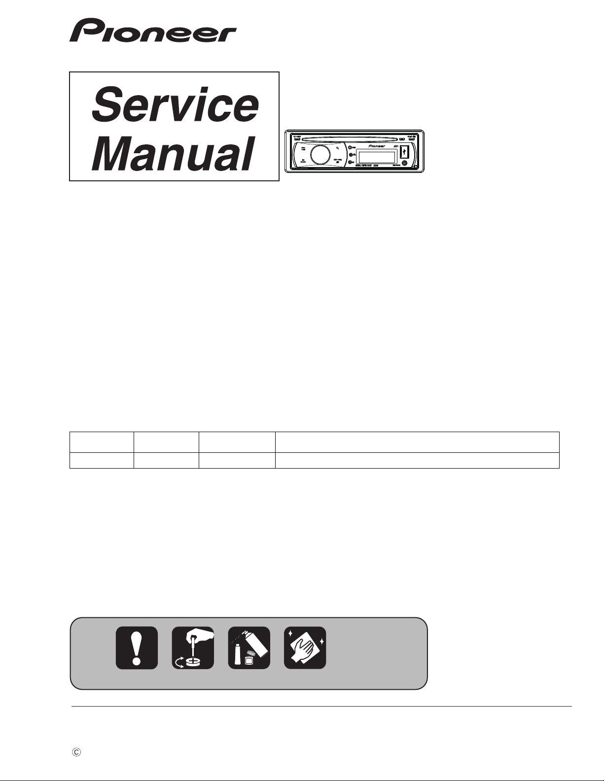
CD RDS RECEIVER
ORDER NO.
CRT4508
DEH-5200SD/XNEW5
DEH-5200SD
CD RECEIVER
DEH-5250SD
DEH-5250SD
DEH-5290SD
This service manual should be used together with the following manual(s):
Model No. Order No. Mech. Module Remarks
CX-3269 CRT4488 S11STD-DOUT CD Mech. Module : Circuit Descriptions, Mech. Descriptions, Disassembly
/XNES
/XNES1
/XNID
/XNEW5
For details, refer to "Important Check Points for Good Servicing".
K-ZZZ. NOV. 2009 Printed in Japan
Page 2
1234
1234
C
D
F
A
B
E
SAFETY INFORMATION
Where in a manufacturer’s service documentation, for example in circuit diagrams or lists
of components, a symbol is used to indicate that a specific component shall be replaced only
by the component specified in that documentation for safety reasons, the following symbol shall
be used:
This service manual is intended for qualified service technicians; it is not meant for the casual do-it-yourselfer.
Qualified technicians have the necessary test equipment and tools, and have been trained to properly and safely repair
complex products such as those covered by this manual.
Improperly performed repairs can adversely affect the safety and reliability of the product and may void the warranty.
If you are not qualified to perform the repair of this product properly and safely, you should not risk trying to do so
and refer the repair to a qualified service technician.
CAUTION:
USE OF CONTROLS OR ADJUSTMENTS OR PERFORMANCE OF PROCEDURES OTHER THAN THOSE
SPECIFIED HEREIN MAY RESULT IN HAZARDOUS RADIATION EXPOSURE.
WARNING!
The AEL (accessible emission level )of the laser power output is less than CLASS 1
but the laser component is capable of emitting radiation exceeding the limit for
CLASS 1.
A specially instructed person should do servicing operation of the apparatus.
Laser diode characteristics
Wave length : 785 nm to 814 nm
Maximum output : 1 190 µW(Emitting period : unlimited)
Additional Laser Caution
Transistors Q101 in PCB drive the laser diodes.
When Q101 is shorted between their terminals, the laser diodes will radiate beam.
If the top cover is removed with no disc loaded while such short-circuit is continued,
the naked eyes may be exposed to the laser beam.
- Safety Precautions for those who Service this Unit.
When checking or adjusting the emitting power of the laser diode exercise caution in order to get safe, reliable
results.
Caution:
1. During repair or tests, minimum distance of 13 cm from the focus lens must be kept.
CAUTION
CLASS 1M INVISIBLE LASER RADIATION WHEN OPEN. DO NOT VIEW DIRECTLY WITH OPTICAL INSTRUMENTS
2. During repair or tests, do not view laser beam for 10 seconds or longer.
2
DEH-5200SD/XNEW5
Page 3
5 678
56
7
8
C
D
F
A
B
E
[Important Check Points for Good Servicing]
In this manual, procedures that must be performed during repairs are marked with the below symbol.
Please be sure to confirm and follow these procedures.
1. Product safety
Please conform to product regulations (such as safety and radiation regulations), and maintain a safe servicing environment by
following the safety instructions described in this manual.
1 Use specified parts for repair.
Use genuine parts. Be sure to use important parts for safety.
2 Do not perform modifications without proper instructions.
Please follow the specified safety methods when modification(addition/change of parts) is required due to interferences such as
radio/TV interference and foreign noise.
3 Make sure the soldering of repaired locations is properly performed.
When you solder while repairing, please be sure that there are no cold solder and other debris.
Soldering should be finished with the proper quantity. (Refer to the example)
4 Make sure the screws are tightly fastened.
Please be sure that all screws are fastened, and that there are no loose screws.
5 Make sure each connectors are correctly inserted.
Please be sure that all connectors are inserted, and that there are no imperfect insertion.
6 Make sure the wiring cables are set to their original state.
Please replace the wiring and cables to the original state after repairs.
In addition, be sure that there are no pinched wires, etc.
7 Make sure screws and soldering scraps do not remain inside the product.
Please check that neither solder debris nor screws remain inside the product.
8 There should be no semi-broken wires, scratches, melting, etc. on the coating of the power cord.
Damaged power cords may lead to fire accidents, so please be sure that there are no damages.
If you find a damaged power cord, please exchange it with a suitable one.
9 There should be no spark traces or similar marks on the power plug.
When spark traces or similar marks are found on the power supply plug, please check the connection and advise on secure
connections and suitable usage. Please exchange the power cord if necessary.
a Safe environment should be secured during servicing.
When you perform repairs, please pay attention to static electricity, furniture, household articles, etc. in order to prevent injuries.
Please pay attention to your surroundings and repair safely.
2. Adjustments
To keep the original performance of the products, optimum adjustments and confirmation of characteristics within specification.
Adjustments should be performed in accordance with the procedures/instructions described in this manual.
4. Cleaning
For parts that require cleaning, such as optical pickups, tape deck heads, lenses and mirrors used in projection monitors, proper
cleaning should be performed to restore their performances.
3. Lubricants, Glues, and Replacement parts
Use grease and adhesives that are equal to the specified substance.
Make sure the proper amount is applied.
5. Shipping mode and Shipping screws
To protect products from damages or failures during transit, the shipping mode should be set or the shipping screws should be
installed before shipment. Please be sure to follow this method especially if it is specified in this manual.
DEH-5200SD/XNEW5
3
Page 4

1234
1234
C
D
F
A
B
E
CONTENTS
SAFETY INFORMATION ..................................................................................................................................... 2
1. SERVICE PRECAUTIONS ............................................................................................................................... 5
1.1 SERVICE PRECAUTIONS......................................................................................................................... 5
1.2 NOTES ON SOLDERING .......................................................................................................................... 6
2. SPECIFICATIONS ............................................................................................................................................ 7
2.1 SPECIFICATIONS...................................................................................................................................... 7
2.2 DISC/CONTENT FORMAT ........................................................................................................................ 9
2.3 PANEL FACILITIES.................................................................................................................................. 10
2.4 CONNECTION DIAGRAM ....................................................................................................................... 12
3. BASIC ITEMS FOR SERVICE........................................................................................................................ 15
3.1 CHECK POINTS AFTER SERVICING..................................................................................................... 15
3.2 PCB LOCATIONS .................................................................................................................................... 16
3.3 JIGS LIST ................................................................................................................................................ 17
3.4 CLEANING............................................................................................................................................... 17
4. BLOCK DIAGRAM.......................................................................................................................................... 18
5. DIAGNOSIS.................................................................................................................................................... 21
5.1 OPERATIONAL FLOWCHART ................................................................................................................ 21
5.2 ERROR CODE LIST ................................................................................................................................ 22
5.3 CONNECTOR FUNCTION DESCRIPTION............................................................................................. 23
6. SERVICE MODE ............................................................................................................................................ 24
6.1 CD TEST MODE...................................................................................................................................... 24
6.2 DISPLAY TEST MODE ............................................................................................................................ 25
7. DISASSEMBLY............................................................................................................................................... 28
8. EACH SETTING AND ADJUSTMENT ........................................................................................................... 35
8.1 CD ADJUSTMENT................................................................................................................................... 35
8.2 CHECKING THE GRATING AFTER CHANGING THE PICKUP UNIT.................................................... 36
8.3 PCL OUTPUT CONFIRMATION.............................................................................................................. 38
9. EXPLODED VIEWS AND PARTS LIST.......................................................................................................... 40
9.1 PACKING ................................................................................................................................................. 40
9.2 EXTERIOR(1) .......................................................................................................................................... 42
9.3 EXTERIOR(2) .......................................................................................................................................... 44
9.4 CD MECHANISM MODULE..................................................................................................................... 46
10. SCHEMATIC DIAGRAM ............................................................................................................................... 48
10.1 TUNER AMP ASSY(MAIN)(GUIDE PAGE)............................................................................................ 48
10.2 TUNER AMP ASSY(MEDIA uCOM)(GUIDE PAGE).............................................................................. 54
10.3 KEYBOARD UNIT.................................................................................................................................. 60
10.4 CD MECHANISM MODULE................................................................................................................... 62
10.5 WAVEFORMS........................................................................................................................................ 64
11. PCB CONNECTION DIAGRAM ................................................................................................................... 66
11.1 TUNER AMP ASSY ............................................................................................................................... 66
11.2 KEYBOARD UNIT.................................................................................................................................. 70
11.3 CD CORE UNIT(S11STD-DOUT).......................................................................................................... 72
12. ELECTRICAL PARTS LIST .......................................................................................................................... 74
4
DEH-5200SD/XNEW5
Page 5
5 678
56
7
8
C
D
F
A
B
E
1. You should conform to the regulations governing the product (safety, radio and noise, and other
regulations), and should keep the safety during servicing by following the safety instructions
described in this manual.
2. Before disassembling the unit, be sure to turn off the power. Unplugging and plugging the connectors
during power-on mode may damage the ICs inside the unit.
3. To protect the pickup unit from electrostatic discharge during servicing, take an appropriate treatment
(shorting-solder) by referring to "the DISASSEMBLY".
4. After replacing the pickup unit, be sure to check the grating.
5. Be careful in handling ICs. Some ICs such as MOS type are so fragile that they can be damaged by
electrostatic induction.
6. On CD Core Unit, actual cable colors and silk print are different.
Green Red
White Black
7. When a CD-DA (regular music CD) is played in the CD test mode, its sound quality will be temporarily
deteriorated. The CD will then repeat normal, deteriorated, normal… playback.
This is due to the difference in the playback modes between the normal operation mode and the CD test
mode, and the interval of generating deteriorated mode and the time taken to return to the normal mode
depend on the error of each clock.
The time taken to turn to the deteriorated mode is at a minimum around 20 seconds while the time to return
to the normal mode is maximum 40 seconds approximately.
Make sure to check the sound quality in the normal operation mode.
8. area and a heat sink becomes hot areas. Be careful not to burn yourself.
1. SERVICE PRECAUTIONS
1.1 SERVICE PRECAUTIONS
DEH-5200SD/XNEW5
5
Page 6

1234
1234
C
D
F
A
B
E
1.2 NOTES ON SOLDERING
For environmental protection, lead-free solder is used on the printed circuit boards mounted in this unit.
Be sure to use lead-free solder and a soldering iron that can meet specifications for use with lead-free solders for repairs
accompanied by reworking of soldering.
Compared with conventional eutectic solders, lead-free solders have higher melting points, by approximately 40 C.
Therefore, for lead-free soldering, the tip temperature of a soldering iron must be set to around 373 C in general, although
the temperature depends on the heat capacity of the PC board on which reworking is required and the weight of the tip of
the soldering iron.
Compared with eutectic solders, lead-free solders have higher bond strengths but slower wetting times and higher melting
temperatures (hard to melt/easy to harden).
The following lead-free solders are available as service parts:
Parts numbers of lead-free solder:
GYP1006 1.0 in dia.
GYP1007 0.6 in dia.
GYP1008 0.3 in dia.
6
DEH-5200SD/XNEW5
Page 7

5 678
56
7
8
C
D
F
A
B
E
2. SPECIFICATIONS
2.1 SPECIFICATIONS
DEH-5200SD/XNEW5
General
Power source ......................... 14.4 V DC (10.8 V to 15.1 V
allowable)
Grounding system................. Negative type
Maximum current consumption
...............................................10.0 A
Back up current ...................... 5.0 mA or less
Dimensions (W × H × D):
DIN
Chassis.................. 180 mm × 50 mm × 165
mm
Nose ....................... 188 mm × 58 mm × 17 mm
D
Chassis.................. 178 mm × 50 mm × 165
mm
Nose ....................... 170 mm × 46 mm × 17 mm
Weight ..................................... 1.3 kg
Audio
Maximum power output ...... 50 W × 4
50 W × 2/4 ohm + 70 W × 1/2
ohm (for subwoofer)
Continuous power output ... 22 W × 4 (50 Hz to 15 000
Hz, 5 % THD, 4 ohm load,
both channels driven)
Load impedance ................... 4 ohm to 8 ohm × 4
4 ohm to 8 ohm × 2
+ 2 ohm × 1
Preout maximum output level
.............................................. 4.0 V
Equalizer (5-Band Graphic Equalizer):
Frequency ......................100/315/1.25k/3.15k/8k Hz
Gain ................................ ±12 dB
HPF:
Frequency ..................... 50/63/80/100/125 Hz
Slope ............................... –12 dB/oct
Subwoofer (mono):
Frequency ..................... 50/63/80/100/125 Hz
Slope ............................... –18 dB/oct
Gain ................................. +6 dB to – 24 dB
Phase .............................. Normal/Reverse
Bass boost:
Gain ................................. +12 dB to 0 dB
CD player
System..................................... Compact disc audio system
Usable discs .......................... Compact disc
Signal-to-noise ratio............. 94 dB (1 kHz) (IEC-A net-
work)
Number of channels ............ 2 (stereo)
MP3 decoding format ......... MPEG-1 & 2 Audio Layer 3
WMA decoding format ....... Ver. 7, 7.1, 8, 9, 10, 11 (2ch
audio)
(Windows Media Player)
AAC decoding format........... MPEG -4 AAC (iTunes en-
coded only) (.m4a)
(Ver. 8.2 and earlier)
WAV signal format................ Linear PCM & MS ADPCM
(Non-compressed)
USB
USB standard specification
............................................... USB 2.0 full speed
Maximum current supply ....500 mA
USB Class .............................. MSC (Mass Storage Class)
File system.............................. FAT12, FAT16, FAT32
MP3 decoding format ..........MPEG-1 & 2 Audio Layer 3
WMA decoding format ....... Ver. 7, 7.1, 8, 9, 10, 11 (2ch
audio)
(Windows Media Player)
AAC decoding format........... MPEG -4 AAC (iTunes en-
coded only) (.m4a)
(Ver. 8.2 and earlier)
WAV signal format................ Linear PCM & MS ADPCM
(Non-compressed)
SD
Compatible physical format
.............................................. Version 2.00
Maximum memory capacity
.............................................. 32 GB (for SD and SDHC)
File system............................. FAT12, FAT16, FAT32
MP3 decoding format ......... MPEG-1 & 2 Audio Layer 3
WMA decoding format ....... Ver. 7, 7.1, 8, 9, 10, 11 (2ch
audio)
(Windows Media Player)
AAC decoding format........... MPEG -4 AAC (iTunes en-
coded only) (.m4a)
(Ver. 8.2 and earlier)
WAV signal format................ Linear PCM & MS ADPCM
(Non-compressed)
FM tuner
Frequency range .................. 87.5 MHz to 108.0 MHz
Usable sensitivity................... 9 dBf (0.8 μV/75 ohm, mono,
S/N: 30 dB)
Signal-to-noise ratio ............ 72 dB (IEC-A network)
MW tuner
Frequency range ................. 531 kHz to 1 602 kHz (9 kHz)
Usable sensitivity................. 25 μV (S/N: 20 dB)
Signal-to-noise ratio ........... 62 dB (IEC-A network)
LW tuner
Frequency range ................ 153 kHz to 281 kHz
Usable sensitivity................. 28 μV (S/N: 20 dB)
Signal-to-noise ratio ........... 62 dB (IEC-A network)
Note
Specifications and the design are subject to modifications without notice.
DEH-5200SD/XNEW5
7
Page 8
1234
1234
C
D
F
A
B
E
WAV signal format................ Linear PCM & MS ADPCM
(Non-compressed)
USB
USB standard specification
............................................... USB 2.0 full speed
Maximum current supply ....500 mA
USB Class............................... MSC (Mass Storage Class)
File system.............................. FAT12, FAT16, FAT32
MP3 decoding format ......... MPEG-1 & 2 Audio Layer 3
WMA decoding format ........ Ver. 7,7.1, 8, 9, 10, 11 (2ch
audio)
(Windows Media Player)
AAC decoding format........... MPEG-4 AAC (iTunes en-
coded only) (.m4a)
(Ver. 8.2 and earlier)
WAV signal format................ Linear PCM & MS ADPCM
(Non-compressed)
SD
Compatible physical format
.............................................. Version 2.00
Maximum memory capacity
.............................................. 32 GB (for SD and SDHC)
File system.............................. FAT12, FAT16, FAT32
MP3 decoding format ......... MPEG-1 & 2 Audio Layer 3
WMA decoding format ........ Ver. 7,7.1, 8, 9, 10, 11 (2ch
audio)
(Windows Media Player)
AAC decoding format.......... MPEG-4 AAC (iTunes en-
coded only) (.m4a)
(Ver. 8.2 and earlier)
WAV signal format................ Linear PCM & MS ADPCM
(Non-compressed)
FM tuner
Frequency range .................. 87.5 MHz to 108.0 MHz
Usable sensitivity................... 9 dBf (0.8 μV/75 ohm, mono,
S/N: 30 dB)
Signal-to-noise ratio ............. 72 dB (IEC-A network)
AM tuner
Frequency range .................. 531 kHz to 1 602 kHz (9 kHz)
530 kHz to 1640 kHz (10
kHz)
Usable sensitivity................... 25 μV (S/N: 20 dB)
Signal-to-noise ratio ............ 62 dB (IEC-A network)
Infrared remote control
Wavelength............................. 940 nm ±50 nm
Output ...................................... typ; 12 mw/sr per Infrared
LED
Note
Specifications and the design are subject to modifications without notice.
General
Rated power source............. 14.4 V DC
(allowable voltage range:
12.0 V to 14.4 V DC)
Grounding system................. Negative type
Maximum current consumption
...............................................10.0 A
Dimensions (W × H × D):
DIN
Chassis.................. 178 mm × 50 mm × 165
mm
Nose ....................... 188 mm × 58 mm × 17 mm
D
Chassis.................. 178 mm × 50 mm × 165
mm
Nose ....................... 170 mm × 46 mm × 17 mm
Weight ..................................... 1.3 kg
Audio
Maximum power output ...... 50 W × 4
50 W × 2/4 ohm + 70 W × 1/2
ohm (for subwoofer)
Continuous power output ... 22 W × 4 (50 Hz to 15 000
Hz, 5 % THD, 4 ohm load,
both channels driven)
Load impedance ................... 4 ohm to 8 ohm × 4
4 ohmto 8 ohm × 2
Preout maximum output level
.............................................. 4.0 V
Equalizer (5-Band Graphic Equalizer):
Frequency ..................... 100/315/1.25k/3.15k/8k Hz
Gain ................................ ±12 dB
HPF:
Frequency ..................... 50/63/80/100/125 Hz
Slope ............................... –12 dB/oct
Subwoofer (mono):
Frequency ..................... 50/63/80/100/125 Hz
Slope ............................... –18 dB/oct
Gain ................................. +6 dB to – 24 dB
Phase .............................. Normal/Reverse
Bass boost:
Gain ................................. +12 dB to 0 dB
CD player
System..................................... Compact disc audio system
Usable discs .......................... Compact disc
Signal-to-noise ratio ............ 94 dB (1 kHz) (IEC-A net-
work)
Number of channels ............ 2 (stereo)
MP3 decoding format ......... MPEG-1 & 2 Audio Layer 3
WMA decoding format ....... Ver. 7, 7.1, 8, 9, 10, 11 (2ch
audio)
(Windows Media Player)
AAC decoding format........... MPEG -4 AAC (iTunes en-
coded only) (.m4a)
(Ver. 8.2 and earlier)
Backup current ...................... 5.0 mA or less
+ 2 ohm × 1
ES, ES1
DEH-5250SD/XNES, DEH-5250SD/XNES1, DEH-5290SD/XNID
8
DEH-5200SD/XNEW5
Page 9
5 678
56
7
8
C
D
F
A
B
E
2.2 DISC/CONTENT FORMAT
DEH-5200SD/XNEW5
9
Page 10
1234
1234
C
D
F
A
B
E
2.3 PANEL FACILITIES
Head unit
traPtraP
TA /NEWS
AUX input jack (3.5
mm stereo jack)
SRC /OFF USB port
(list) / iPod
S.Rtrv
/ LOC
Disc loading slot DISP/ / SCRL
(eject)
MULTI-CONTROL
(M.C.)
MUTE / CLK BAND / ESC
Detach button
SD memory card
slot
You can see the SD
memory card slot if
you remove the
front panel.
CAUTION
Use an optional Pioneer USB cable (CD-U50E) to
connect the USB audio player/USB memory to
the USB port. Since the USB audio player/USB
memory is projected forward from the unit, it is
dangerous to connect directly.
Do not use the unauthorized product.
Optional remote control
The remote control CD-R320 is sold separately.
Part Operation
VOLUME
Press to increase or decrease volume.
MUTE
Press to mute. Press again to unmute.
/ / /
Press to perform manual seek
tuning, fast forward, reverse and
track search controls.
Also used for controlling functions.
AUDIO Press to select an audio function.
DISP/ SCRL
Press to select different displays.
Press and hold to scroll through
the text information.
Press to pause or resume.
FUNCTION
Press to select functions.
Press and hold to recall the initial
setting menu when the sources
are off.
LIST /
ENTER
Press to display the disc title,
track title, folder, or file list depending on the source.
While in the operating menu,
press to control functions.
DEH-5200SD/XNEW5
Fastening the front panel
If you do not plan to detach the front panel,
the front panel can be fastened with supplied
screw.
Screw
BPZ20P060FTC
10
DEH-5200SD/XNEW5
Page 11
5 678
56
7
8
C
D
F
A
B
E
1
253
4
6
7
98abcde
f
g
h
o
m
2fi
l
k
n
j
DEH-5250SD/XNES, DEH-5250SD/XNES1, DEH-5290SD/XNID
Head unit
traPtraP
1 SW/ BASS 9
2 SRC /OFF a USB port
3
4 S.Rtrv c
5 Disc loading slot d DISP/
6
7 CLK / DISP OFF f BAND /ESC
8 Detach button g
(list) b / iPod
(eject) e
CAUTION
Use an optional Pioneer USB cable (CD-U50E) to
connect the USB audio player/USB memory to
the USB port. Since the USB audio player/USB
memory is projected forward from the unit, it is
dangerous to connect directly.
Do not use the unauthorized product.
AUX input jack (3.5
mm stereo jack)
/ LOC
/ SCRL
MULTI-CONTROL
(M.C.)
SD memory card
slot
You can see the SD
memory card slot if
you remove the
front panel.
Remote control
Part Operation
h VOLUME
i MUTE
j
/ / /
k AUDIO Press to select an audio function.
l DISP/ SCRL
m
n FUNCTION
LIST/
o
ENTER
Press to increase or decrease volume.
Press to mute. Press again to unmute.
Press to perform manual seek
tuning, fast forward, reverse and
track search controls.
Also used for controlling functions.
Press to select different displays.
Press and hold to scroll through
the text information.
Press to pause or resume.
Press to select functions.
Press and hold to recall the initial
setting menu when the sources
are off.
Press to display the disc title,
track title, folder, or file list depending on the source.
While in the operating menu,
press to control functions.
DEH-5200SD/XNEW5
11
Page 12
1234
1234
C
D
F
A
B
E
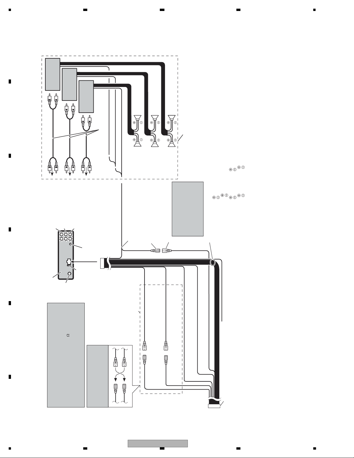
2.4 CONNECTION DIAGRAM
2* 1*
3*4*
9. Note
Depending on the kind of vehicle,
the function of 2* and 4* may be
different. In this case, be sure to
connect 1* to 4* and 3* to 2*.
10. Connect leads of the
same color to each other.
11. Yellow (2*)
Back-up (or
accessory)
13. Red (4*)
Accessory
(or back-up)
12. Yellow (1*)
Connect to the constant
12 V supply terminal.
14. Red (3*)
Connect to terminal controlled by
ignition switch (12 V DC).
16. Black (chassis ground)
Connect to a clean, paint-free metal location.
17. ISO connector
Note
In some vehicles, the ISO connector may be
divided into two. In this case, be sure to
connect to both connectors.
18. Yellow/black
If you use an equipment with Mute
function, wire this lead to the Audio Mute
lead on that equipment. If not, keep the
Audio Mute lead free of any connections.
8. Notes
• Change the initial setting of this unit (refer to the
operation manual). The subwoofer output of this unit is
monaural.
• When using a subwoofer of 70 W (2
), be sure to
connect with Violet and Violet/black leads of this unit.
Do not connect anything with Green and Green/black
leads.
15. Orange/white
Connect to lighting switch terminal.
1. This product
7. Antenna
jack
6. Fuse (10 A)
5. Wired remote input
Hard-wired remote
control adaptor can
be connected (sold
separately).
26. Power amp
(sold separately)
27. Connect with RCA cables
(sold separately)
28. System remote control
26. Power amp
(sold separately)
26. Power amp
(sold separately)
24. To front output
23. To rear output
31. Rear speaker
29. Subwoofer
30. Front speaker
31. Rear speaker
29. Subwoofer
30. Front speaker
25. To subwoofer output
32. Perform these connections when
using the optional amplifier.
22. Speaker leads
White: Front left
White/black: Front left
Gray: Front right
Gray/black: Front right
Green: Rear left or subwoofer
Green/black:Rear left or subwoofer
Violet: Rear right or subwoofer
Violet/black: Rear right or subwoofer
19. Blue/white
Connect to system control
terminal of the power amp (max.
300 mA 12 V DC).
20. Blue/white (6*)
Connect to auto-antenna relay
control terminal (max. 300 mA
12 V DC).
The pin position of the ISO
connector will differ depending
on the type of vehicle. Connect
5* and 6* when Pin 5 is an
antenna control type. In another
type of vehicle, never connect
5* and 6*.
21. Blue/white (5*)
Hcb
2. Rear output
4. Subwoofer output
3. Front output
DEH-5200SD/XNEW5
12
DEH-5200SD/XNEW5
Page 13
5 678
56
7
8
C
D
F
A
B
E
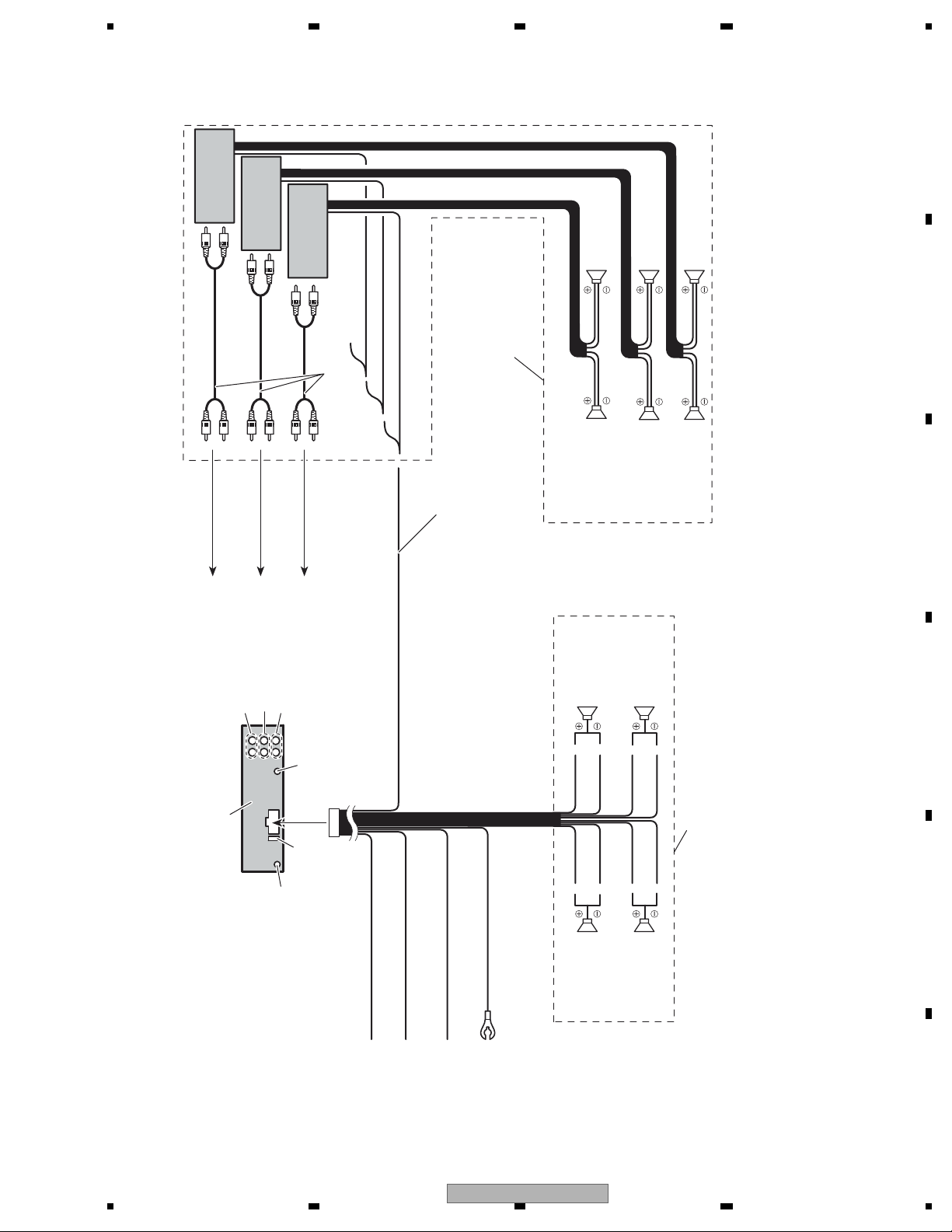
DEH-5250SD/XNES, DEH-5250SD/XNES1, DEH-5290SD/XNID
(sold separately)
29. Power amp
(sold separately)
29. Power amp
29. Power amp
(sold separately)
33. Subwoofer33. Subwoofer
16. Front speaker
23. Rear speaker23. Rear speaker
25. To rear output
2. Rear output
26. To front output
27. To subwoofer output
3. Front output
4. Subwoofer output
Hard-wired remote control adaptor
5. Wired remote input
(sold separately)
28. Connect with RCA cables
31. System remote control
Connect to system control terminal of the
power amp or auto-antenna relay control
30. Blue/white
can be connected (sold separately).
when using the optional
amplifier.
32. Perform these connections
terminal (max. 300 mA 12 V DC).
16. Front speaker
16. Front speaker
18.Right17.Left
23. Rear speaker
1. This product
6. Fuse (10 A)
7. Antenna
jack
Connect to the constant 12 V supply terminal.
8. Yellow
9. Red
Connect to lighting switch terminal.
Connect to terminal controlled by ignition
switch (12 V DC).
10. Orange/white
DEH-5200SD/XNEW5
Connect to a clean, paint-free metal location.
11. Black (chassis ground)
12. White 14. Gray
16. Front speaker
15. Gray/black13. White/black
19. Green 21. Violet
20. Green/black 22. Violet/black
23. Rear speaker
anything to the speaker leads that are
not connected to speakers.
24. With a 2 speaker system, do not connect
13
Page 14
1234
1234
C
D
F
A
B
E
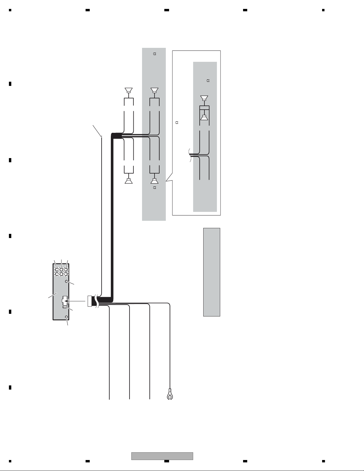
34. Note
Change the initial setting of this unit.
The subwoofer output of this unit is monaural.
1. This product
3. Front output
4. Subwoofer output
6. Fuse (10 A)
2. Rear output
7. Antenna
jack
5. Wired remote input
Hard-wired remote control adaptor
can be connected (sold separately).
8. Yellow
Connect to the constant 12 V supply terminal.
9. Red
Connect to terminal controlled by ignition
switch (12 V DC).
10. Orange/white
Connect to lighting switch terminal.
11. Black (chassis ground)
Connect to a clean, paint-free metal location.
35. Subwoofer (4 )
36. When using a subwoofer of 70 W (2
), be sure to connect
with Violet and Violet/black leads of this unit.
Do not connect anything with Green and Green/black leads.
38. Subwoofer
(4
)x 2
37. Not used.
17. Left 18. Right
16. Front speaker
12. White 14. Gray
15. Gray/black13. White/black
19. Green 21. Violet
20. Green/black 22. Violet/black
16. Front speaker
30. Blue/white
Connect to system control
terminal of the power amp or
auto-antenna relay control
terminal (max. 300 mA 12 V DC).
35. Subwoofer (4
)
19. Green 21. Violet
20. Green/black 22. Violet/black
14
DEH-5200SD/XNEW5
Page 15
5 678
56
7
8
C
D
F
A
B
E
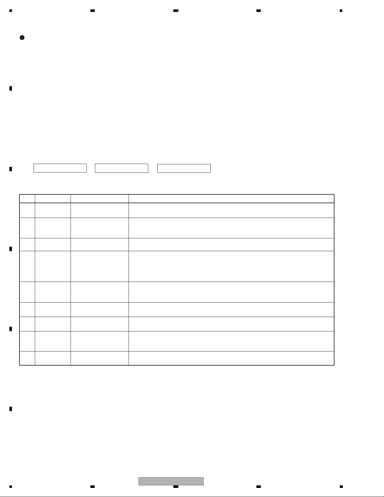
demrifnocebotmetIserudecorP.oN
1 Confirm whether the customer complain has
been solved.
If the customer complain occurs with the
specific media, use it for the operation check.
The customer complain must not be
reappeared.
Display, audio and operations must be
normal.
2 CD Play back a CD.
(Track search)
No malfunction on display, audio and
operation.
3 FM/AM tuner Check FM/AM tuner action.
(Seek, Preset)
Switch band to check both FM and AM.
Display, audio and operations must be
normal.
4 Check whether no disc is inside the product. The media used for the operating check must
be ejected.
retfaecnaraeppastinotridrosehctarcsoNkcehcecnaraeppA5
receiving it for service.
Item to be checked regarding audio
3. BASIC ITEMS FOR SERVICE
3.1 CHECK POINTS AFTER SERVICING
To keep the product quality after servicing, please confirm following check points.
See the table below for the items to be checked regarding audio:
Distortion
Noise
Volume too low
Volume too high
Volume fluctuating
Sound interrupted
DEH-5200SD/XNEW5
15
Page 16
1234
1234
C
D
F
A
B
E
3.2 PCB LOCATIONS
A
B
Keyboard Unit
CD Core Unit (S11STD-DOUT)
C
Tuner Amp Assy
A:DEH-5200SD/XNEW5
B:DEH-5250SD/XNES
C:DEH-5250SD/XNES1
D:DEH-5290SD/XNID
Unit Number : QWM3122(A)
Unit Number : QWM3123(B,C,D)
Unit Name : Tuner Amp Assy
Unit Number :
Unit Name : Keyboard Unit
Unit Number : CWX3774
Unit Name : CD Core Unit(S11STD-DOUT)
16
DEH-5200SD/XNEW5
Page 17
5 678
56
7
8
C
D
F
A
B
E
- Jigs List
Name
Test Disc
L.P.F.
Jig No.
TCD-782
Remarks
Checking the grating
Checking the grating (Two pieces)
Name
Jig
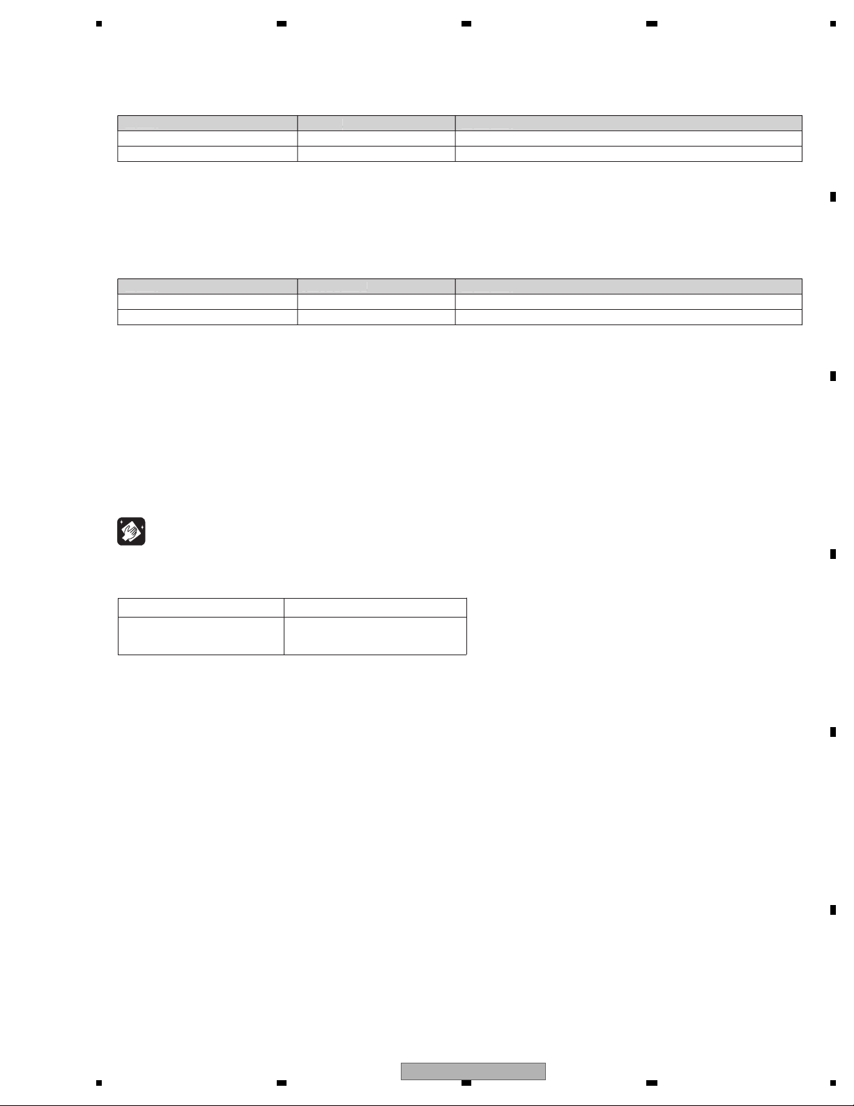
- Grease List
Name
Grease
Grease
Grease No.
GEM1024
GEM1045
Remarks
CD Mechanism Module
CD Mechanism Module
e
Before shipping out the product, be sure to clean the
following portions by using the prescribed cleaning
tools:
Portions to be cleaned Cleaning tools
CD pickup lenses Cleaning liquid : GEM1004
Cleaning paper : GED-008
3.3 JIGS LIST
m
3.4 CLEANING
No.
rease No.
emarks
emarks
DEH-5200SD/XNEW5
17
Page 18
1234
1234
C
D
F
A
B
E
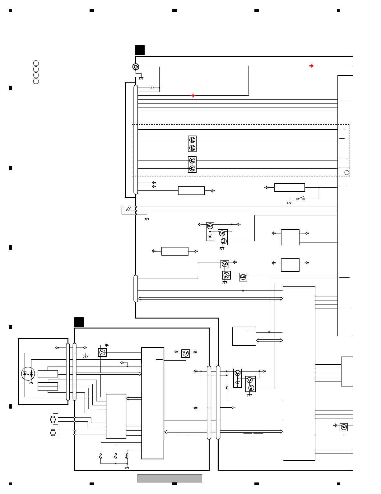
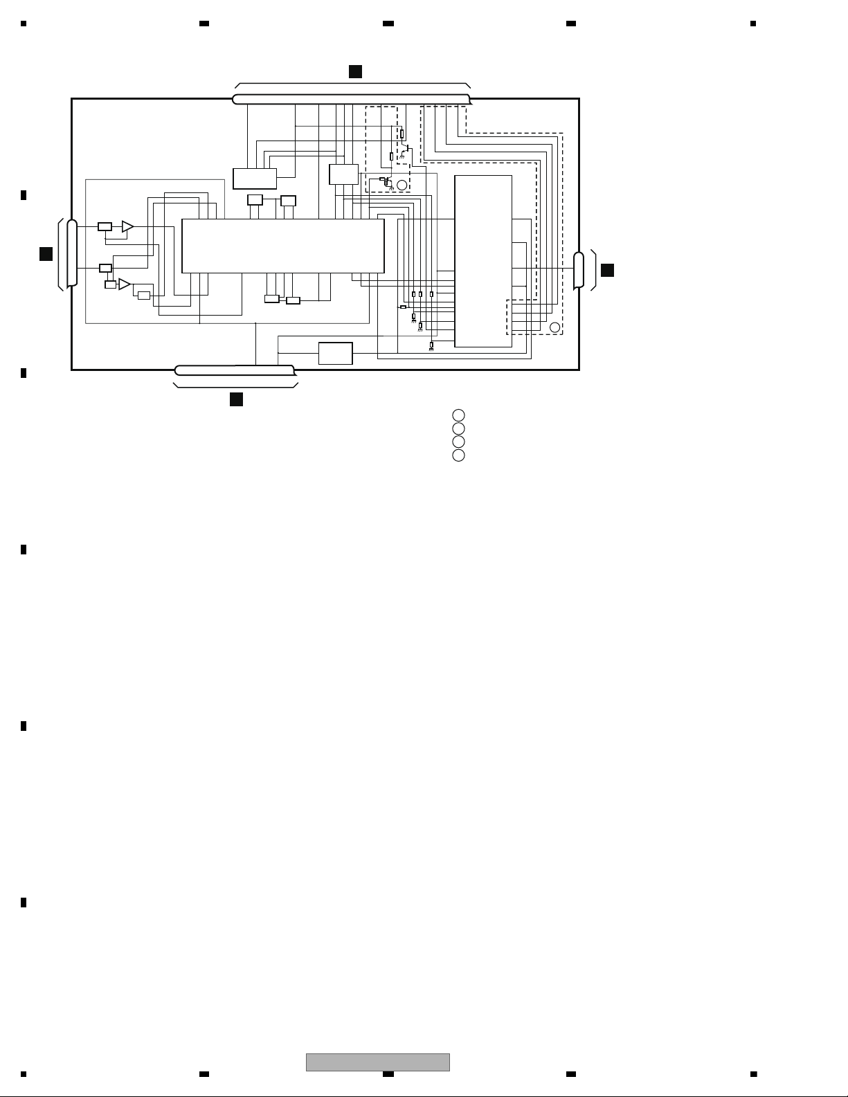
4. BLOCK DIAGRAM
M
M
IC6
COMP
PEG645B
PEG647A
SYSTEM
BUP
VDD5V
Q901
Q902
35
DALMON
10
RESET
12
S-80827CNNB-B8M
IC651
RESET
VDD3.3V
S652
:DEH-5200SD/XNEW5
:DEH-5250SD/XNES
A
:DEH-5250SD/XNES1
:DEH-5290SD/XNID
C
B
B
JA401
JA661
ANTENNA
SD CARD
SL
FM/AM TUNER UNIT
VCC
FMANT
AMANT
1
3
5
CE2
6
CE1
8
CK
9
DI
10
LDET
11
DO
14
RDS_CK
18
RDS_DATA
19
4
SYS8V
TUNER AMP ASSY
A
C
Q402
RDS_LOCK
20
RDS_HSLK
21
Q401
ROM_VDD
13
VDD3.3V
VDD_3.3
17
Lch TUNL
23
SYS8V
3 1
NJM2885DL1-33
IC431
TUNER3V REG.
USB5V DD5V
5 4
R5523N001B
IC151
USB5V REG.
VOUT VIN
1
EN
3
FLG
DD5V BUP
21
BD9781HFP
IC161
DD5V REG.
SW VIN
7
EN
VDD3.3V
32
92
KEYAD
34
MEDRX
33
MEDTX
43
MEDMUTE
41
MEDSTBY
KEYD
63
95
SL
RCK
RDS57K
MEDRST
64
TUNPCE1
TUNPCE2
65
TUNPCK
66
72
LDET
TUNPDI
67
71
TUNPDO
77
RDSDT
RDSLK
74
78
21
USBCTL
23
USBFLG
24
42
80
SDCTL
19
VDCONT
SYNC
SD_DATA0 - SD_DATA3, SD_CLK, SD_CMD
R5S7262ZD144FPU
IC501
CN701
CN781
MEDIA uCOM
114
SD_CD
113
CDRST
RESET
16
15
8
VD
9
VDD
VDD
CD
4
12
MED3.3V
Q781
Q491
Q782
63
SYS_TXD
61
59
58
BRST
MEDIA_MUTE
SYS_RXD
71
70
DM
DP
148
CP_SDA
149
CP_SCL
112
CPRST
111
CPPWR
MED3.3V
PICKUP UNIT
(P10.5)(SERVICE)
CD CORE UNIT(S11STD-DOUT)
A
LD
MD
LD-
MD
HOLOGRAM
UNIT
LD+
FOCUS ACT.
TRACKING ACT.
FOP
TOP
VREF
FOM
TOM
VCC
VCC
15
5
14
15
5
212
1
14
88
33
44
1212
RF AMP, CD DECODER, MP3&WMA DECODER
DIGITAL SERVO/DATA•PROCESSOR
CPU, USB HOST CONTROLLER
PE5706A
IC201
Q101
IC301
BA5839FP
ACTUATOR/
MOTOR DRIVER
CN101
TD,FD
AC,BD,E,F
1
2
VDD
TOP
FOP
REFO
93
FOM
TOM
PD
REFO
V+3A
LD+
GND
SPINDLE
MOTOR
LOADING/CARRIAGE
MOTOR
21
9
SD,MD
40
39
22
41
15
VO3+
16
VO3-
17
VO4+
18
VO4-
11
VO1-
14
VO2+
12
VO1+
13
VO2-
SOM
SOP
LCOM
LCOP
CNT
MUTE
LOIN
S903
S901
S905
DSCSNS HOME8SNS
35
37
38
LD
PD
CONT
CLCONT
HOME
8SNS
DSCSNS
RESET
REFOUT
LOEJ
PUEN
CN701
2
VD
1
Q102
54
V+3A
VDD
CD DATA (CDSRQ,CDSTBY,SKIP,
29
RESET
SCL,SDA,DATA,BCLK,LRCK,WAIT)
9
8
2,3
VDD5V REG.
SD3.3V REG.
KEYAD
KEYD
2
3
VDD5V
VDD3.3V
3 1
NJM2885DL1-33
IC901
VDD3.3V REG.
CWW1967
IC581
FLASH ROM 16Mbit
12
RESET
43
RESET
VD
85
VDSENS
BUP
Q751
Q752
MECHA VD
CD DATA (CDSRQ,CDSTBY,SKIP,
SCL,SDA,DATA,BCLK,LRCK,WAIT)
138
DACLRCK
137
DACDATA
139
105
136
DACCLK
DEEMPH
DACSCK
WM87
IC1
DA
1
LRCKIN
2
DIN
3
BCKIN
12
DEEMPH
14
MCLK
WIRED REMOTE
1
VDD
1
GND
Q783
18
DEH-5200SD/XNEW5
Page 19
5 678
56
7
8
C
D
F
A
B
E
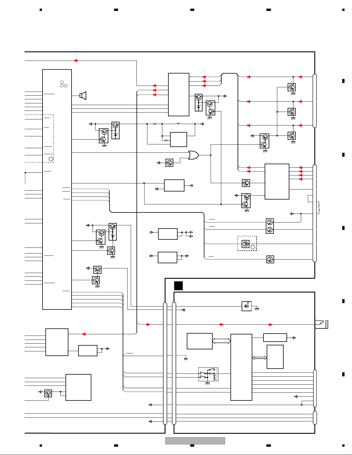
IC601
COMPUTER
A
PEG645B8:
B
PEG647A8:
SYSTEM MICRO
35
DALMON
A
10
RESET
Q381
BUP
BUP
TELIN
ISENS
ASENS
BSENS
CN801
RCA OUT
KYDT
DPDT
ROT1
ROT0
3
8
11
16
19
6
10
12
14
USBDP
USBDM
15
13
VBUS
USB5V
OEL+B
AUXL
BUP OEL+B
Q851
Q852
BUP
PM9012A
IC201
E.VOL
25
OUTFL
26
FL
RL
OUTRL
36TUNL
35CDL
S5B+L
27 SWL
OUTPL
39AUXL
S1Q+L
S4B-L
21
22
CLK
STB
23
DATA
PA2030A
IC351
AMP
9
OUT1(+)
7FL-
OUT1(-)
12RL
SYSPW
11FL
IN1
FL
5RL+
OUT2(+)
3 RL-
OUT2(-)
25 BREM
H-SW/VDS-DET
IN2
22
MUTE
4
STBY
48
MUTE
32
92
KEYAD
16
18
40
TELIN
34
MEDRX
33
MEDTX
43
MEDMUTE
41
MEDSTBY
KEYD
63
95
SL
RCK
RDS57K
MEDRST
ISENS
ASENS
BSENS
64
TUNPCE1
TUNPCE2
65
TUNPCK
66
72
LDET
TUNPDI
67
71
TUNPDO
77
RDSDT
RDSLK
74
78
55
VST
54
VCK
53
VDT
50
OELPW
VDD3.3V
Q841
Q842
47
SWVDD
51
DIMMER
49
ILMPW
21
USBCTL
23
USBFLG
24
42
80
SDCTL
19
VDCONT
SYNC
JA301
SWL
4
2
JA981
FL+
1
3
5
7
18
14
B.UP
15
17
ACC
13
TEL
9
6
RL
FL
SWL
RL
Q302
Q301
Q303
Q361
ILL
11
Q951
Q931
Q382
VDD5V
Q351
Q921
Q491
2
341S2162
IC491
iPod CP
13
I2C_SDA/SPI_SOMI
12
I2C_SCL/SPI_SIMO
1
4
nRESET
5
VCC
2
MODE1/SPI_nSS
MED3.3V
8
1
7
NJM2360AM
IC851
CSSI
8
CD
6
V+
BUP
Q821
Q822
Q823
KEYBOARD UNIT
B
30
KYDT
29
DPDT
1
ROT1
2
ROT0
A
C
20
PEE
BUZZER
BZ601
OEL9V REG.
OEL+B
OEL+B
Q242
Q241
VP+B
20
VCCH
ILM+B
SWVDD
MED3.3V DD5V
VDD5V
16
S-1172B33-E6
IC591
MED3.3V REG.
VOUT VIN
3
ON/OFF
MED1.2V MED3.3V
4
3
BH12PB3WHFV
IC592
MED1.2V REG.
VOUT VIN
1
STBY
DSENS
17
5
1
NJM2872F05
IC182
DAC5V REG.
SYS8V
WM8761GED
IC181
DAC
9
VOUTL
CDL
1
LRCKIN
2
DIN
3
BCKIN
12
DEEMPH
14
MCLK
8
VDD
VIN
3
CONT
VOUT
ILM+B
SWVDD
SOURCE CONNECTOR
B.UP
BSENS
ASENS
TELMUTE
ISENS
3
16
CN1801
JA1806
SWVDD
ILLUMI
ILM+B
FRONT AUX
AUXL
AUXR
AUXGND
3
2
1
19
AUXL
ROT0
14
S1821
ROTARY COMMANDER
ROT112Phase_A
Phase_B
88
KEY MATRIX
DSENS
20
KD0-3,KS0-2
8
11
OEL+B
VBUS
6
KYDT
10
DPDT
15
USBDP
13
USBDM
28
27
SWVDD
KYDT
DPDT
O_CIN
O_SID
O_SCLK
O_DC
O_RST
O_CSB
REM
4
13
GP1UXC14RK
IC1861
JOYST
IC1871
COMPUTER
PEG652A8
PD8192B9
IC1872
ROM
CONTROL SENSOR
REMOTE
MICRO
CN1811
4
USBDP
3
USBDM
2
USB5V
SWVDD
26
33
35
22
24
23
CN1921
8
OSCIN
7
D7(SDIN)
6
D6(SCLK)
12
VCC
2
11
VDD
5
DC
4
RSTB
3
CSB
USB
VCC
OEL MODULE
DSENS
20
DSENS
SYS8V
BUP
2
1
NJM2388F84
IC911
SYS8V REG.
VOUT
VIN
4
CONTROL
SYSPW
36
DEH-5200SD/XNEW5
19
Page 20
1234
1234
C
D
F
A
B
E
FMRF
ANT adj
RF adj
FM ANT
T51
CF52
RFGND
OSCGND
DGND
AUDIOGNDNCVCC
VDD_3.3
3.3V
2.5V
IC4
2.5V
IC2
NC
CE2
ROM_VDD
SL
DI
CK
CE1
LDET
DO
RDS_CK
RDS_DATA
RDS_LOCK
RDS_HSLK
76 13 5 1098 11 14 18192021
1
3
212 1522 16 4 17
IC1
3.3V
AM ANT
FMRF
ATT
LPF
OSC
IC3
EEPROM 5.0V
IC5
ATT
MIXER, IF AMP
DET, FM MPX,
RDS DECODER
23
Lch
FM/AM TUNER UNIT
A
A
A
A
3.3V→2.5V
5V→3.3V
:DEH-5200SD/XNEW5
:DEH-5250SD/XNES
A
:DEH-5250SD/XNES1
:DEH-5290SD/XNID
C
B
B
A
A
20
DEH-5200SD/XNEW5
Page 21
5 678
56
7
8
C
D
F
A
B
E
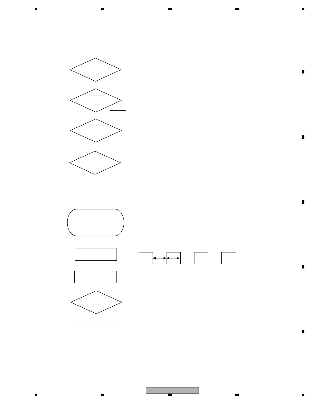
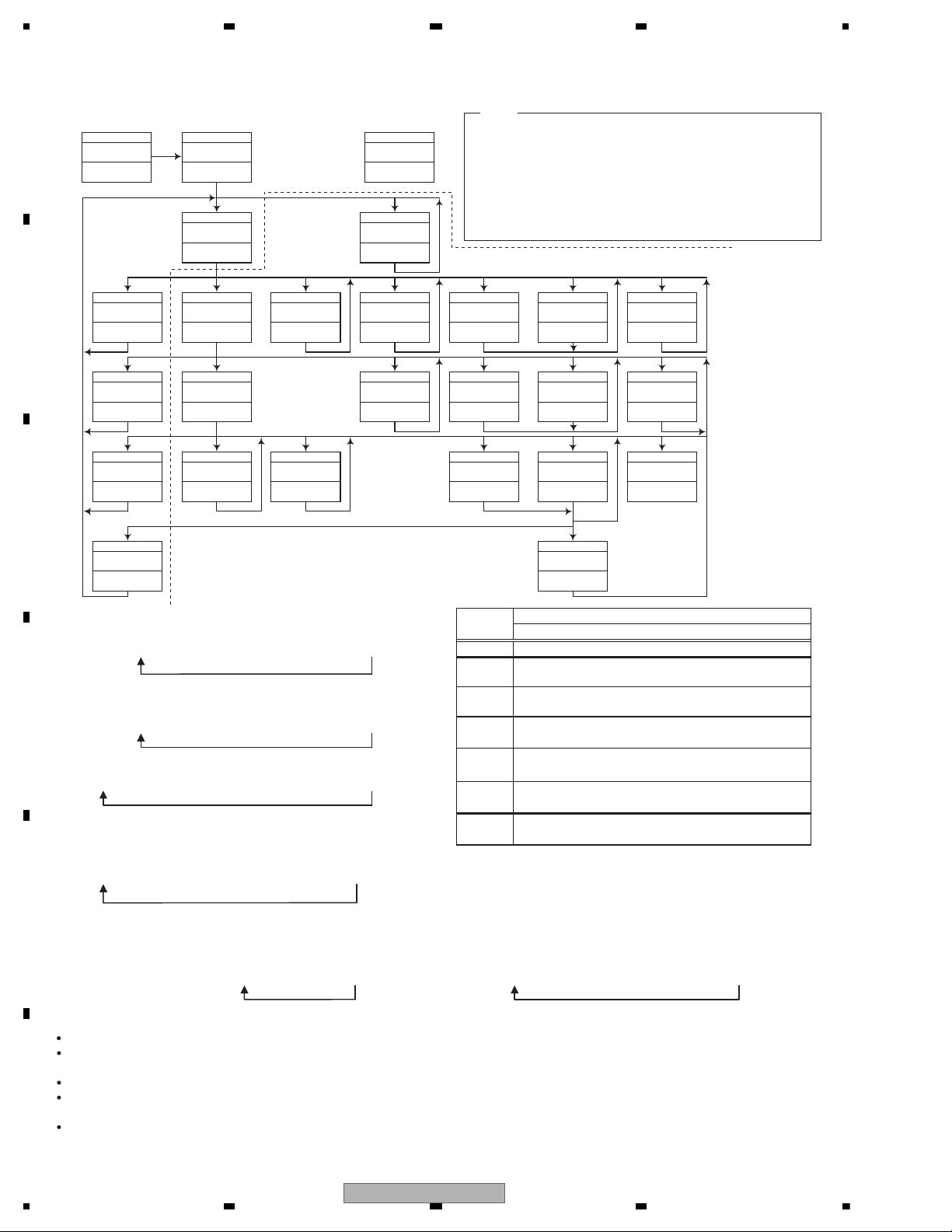
Vcc = 3.3 V
Pin 14
BSENS
Pin 16
ASENS
Pin 18
DSENS
Pin 17
BSENS = L
ASENS = L
Starts
communication
with Grille
microcom
p
uter.
SWVDD <- H
Pin 47
Source keys
operative
Source ON
SYSPW <- H
Pin 36
500 ms
500 ms
In case of the above signal, the communication
with Grille microcomputer may fail.
If the time interval is not 500 msec, the oscillator
may be defective.
Completes power-on operation.
(After that, proceed to each source operation)
Power ON
5. DIAGNOSIS
5.1 OPERATIONAL FLOWCHART
DEH-5200SD/XNEW5
21
Page 22
1234
1234
C
D
F
A
B
E
5.2 ERROR CODE LIST
8-digit display 6-digit display 4-digit display
ERROR-xx ERR-xx E-xx
(2) LIST OF CD ERROR CODES (Error Mode: 0xFD)
Code Classification
Error code to be displayed
Details and possible causes
10 Servo Carriage Home NG The CRG cannot move toward the inner track.
The CRG cannot move from the inner track.
--> Defective HOME SW; Failure in CRG movement.
7
Servo TOC reading NG TOC information cannot be read.
--> The partial disk or TOC content is illegal.
11
Servo Focus Search NG Focusing not available
--> Disc placed upside-down; Stains on the disc; excessive vibration.
17 Servo Setup NG AGC protection does not work. Focus can be easily lost.
--> Scratches or stains on the disc; excessive vibration.
15 Servo Failure in RF data RF not read
--> A CD-R disc that does not contain data loaded
--> A CD-RW disc that does not contain data loaded
12
Servo Spindle Lock NG
Subcode NG
RF-amp NG
Spindle not locked. Subcode not readable.
Proper RF AMP gain not obtained.
--> Defective spindle; Scratches or stains on the disc; excessive vibration.
-->
A CD-R disc that does not contain data loaded, or in a rare case, disc placed upside-down.
--> CD signal error.
30
Servo Search Time Out Failed to reach a target address
--> CRG tracking error; Scratches on the disc; Stains on the disc
50 Mechanism Failure in ejection
Load NG
Disc ejection not completed
Disc loading not completed
--> A foreign object inserted in the mechanism; Disc jammed.
51
Mechanism Failure in retried
turning for ejection
Disc could not be ejected even after disc turning had been retried.
--> A foreign object inserted in the mechanism; Disc jammed.
NOTES
• Indications of error codes are available only during disc operations, because CD operations are
unavailable if a mechanical error is generated.
• If the TOC cannot be read, this is not processed as an error, and operation continues accordingly.
• If you design a new head unit, be sure to use one of the display formats indicated in “Display example of
the main unit.”
ERROR CODES
(1) DISPLAY METHOD
If “0xFD” error mode is displayed in CD MODE (CD MODE area for display), an error code will be displayed in the MIN (minute
display) and SEC (second display) areas.
The same code is displayed in the MIN and SEC areas.
The TNO area is blank (#0FFH), as it conventionally was.
• Display example of the main unit
Depending on the display capability of LCDs, the display format varies, as shown below. XX denotes an error number.
Note: In a case of an OEM product, the error display format is subject to the specifications used by the equipment
manufacturer.
If a CD memory device is inoperable, or operation of such media is stopped by an error, the error mode is established and a
cause of the error is displayed by an error code. Indication of error codes is intended to reduce the number of calls from
customers and facilitate failure analysis and repair work in servicing.
• The 2 high-order digits of an error code denote the main
classification, shown below.
0x: Servo-related errors
1x: Servo-related errors
3x: Servo-related errors
5x: Mechanism-related errors
• How to restore from each error is shown below.
0x, 1x and 3x: ACC-OFF then ON, CD-OFF then ON,
Disc ejection
5X: ACC-OFF then ON, Disc ejection, Disc reloading
22
DEH-5200SD/XNEW5
Page 23
5 678
56
7
8
C
D
F
A
B
E
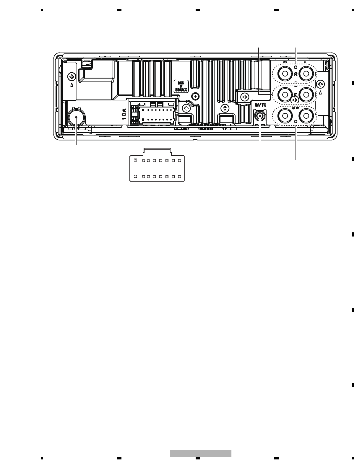
ANTENNA
REAR
OUTPUT
16
14 12 108642
15
13 11 97531
1. FL+
2. FR+
3. FL-
4. FR-
5. RL+
6. RR+
7. RL-
8. RR-
9. TEL
10. NC
11. ILL
12. A.ANT
13. ACC
14. BREM
15. B.UP
16. GND
WIRED REMOTE
CONTROL
SUBWOOFER
OUTPUT
FRONT
OUTPUT
5.3 CONNECTOR FUNCTION DESCRIPTION
DEH-5200SD/XNEW5
23
Page 24
1234
1234
C
D
F
A
B
E
6. SERVICE MODE
[Key]
Contents
Display
[BAND]
Power On
(T.Offset is adjusted)
TRK MIN SEC
00 00 00
[2]
RF AMP
Gain switching
GG GG GG
*1
[3]
Focus Close
S curve check
TRK MIN SEC
91 91 91
[6]
Focus Mode switching
0X 0X 0X
*2
[1]
Tracking Servo
Close
00 00 00
or 99 99 99
[<]
CRG +
[2]
Self-adjusting
switching
TRK MIN SEC
?? ?? ??
*3*8
[>]
CRG -
*8
[BAND]
Power Off
TRK MIN SEC
[BAND]
Power Off
TRK MIN SEC
[BAND]
Power Off
TRK MIN SEC
[BAND]
Power Off
TRK MIN SEC
[1]
T.Close & AGC
Applicable servomechanism
TRK MIN SEC
?tr ?min ?sec
[3]
RF AGC /
RF AGC coefficient display
[<]
CRG +
8X 8X 8X
or 9X 9X 9X
[2]
T.Balance adjustment /
T.BAL coefficient display
TRK MIN SEC
?? ?? ??
[>]
CRG -
?? ?? ??
[1]
F,T,RF AGC
F.Bias display switching
TRK MIN SEC
TRK MIN SEC
TRK MIN SEC
[3] [<]
CRG/TR Jump +
[2]
Tracking Open
[>]
CRG/TR Jump -
?tr ?min ?sec
TRK MIN SEC
TRK MIN SEC
00 00 00
or 99 99 99
TRK MIN SEC
?tr ?min ?sec
8X 8X 8X
or 9X 9X 9X
8X 8X 8X
or 9X 9X 9X
00 00 00
or 99 99 99
TRK MIN SEC
?tr ?min ?sec?? ?? ??
*7
F,T AGC / F.Bias
RF AGC
8X 8X 8X
or 9X 9X 9X
[2]
Tracking Open
*6
*4 *4
Operation
[Key]
Test Mode
[BAND] Power On/Off
[<]
CRG + / TR Jump +
(Direction of the external surface)
[>]
CRG - / TR Jump (Direction of the internal surface)
[1] T. CLS & AGC & Applicable servomechanism /
AGC,AGC display setting
[2] RF Gain switching / Offset adjustment display /
T.Balance adjustment / T. Open
[3] F. Close,S. Curve / Rough Servo and RF AGC /
F,T,RF AGC
[6] F. Mode switching / Tracking Close
After the [EJECT] key is pressed keys other than the [EJECT] key should not be pressed, until disc ejection is complete.
When the key [2] or [3] is pressed during the Focus Search, the power supply should be immediately turned off (otherwise the lens sticks
to Wall, causing the actuator to be damaged).
100TR Jump, the mechanism shall be set to the Tracking Close mode when the key is released.
When the power is turned on/off the gain of the RFAMP is reset to 0 dB. At the same time all the self-adjusting values shall return to the
default setting.
Do not do Tracking Servo Close before doing Focus Servo Close. (Because the overcurrent flows)
- Flow Chart
[CD] or [SOURCE]
Source ON
TRK MIN
[BAND] + [RDM] -> Reset
Test Mode IN
NOTE
When a CD-DA (regular music CD) is played in the CD test mode, its sound quality
will be temporarily deteriorated. The CD will then repeat normal, deteriorated,
normal… playback.
This is due to the difference in the playback modes between the normal operation
mode and the CD test mode, and the interval of generating deteriorated mode and
the time taken to return to the normal mode depend on the error of each clock.
The time taken to turn to the deteriorated mode is at a minimum around 20
seconds while the time to return to the normal mode is maximum 40 seconds
approximately.
Make sure to check the sound quality in the normal operation mode.
*1) TYP t + 6 dB t + 12 dB
TRK
MIN
SEC
TRK06MIN06SEC
06
TRK12MIN12SEC
12
*2) Focus Close
t S. Curve t F EQ measurement setting
TRK00MIN00SEC
00
TRK
01
MIN01SEC
01
TRK02MIN02SEC
02
(
TRK99MIN99SEC
99)
*3) F.Offset Display t T.Offset Display t Switch to the
order of the original display
*4) 100TR Jump
*7) TRK/MIN/SEC
t F.AGC t T.AGC Gain t F.Bias t RF AGC
*8) CRG motor voltage = 2 [V]
*9) TYP (1X)
t 2X t 1X
TRK
MIN
SEC
TRK
22
MIN22SEC
22
TRK11MIN11SEC
11
*10) OFF(TYP)
t FORCUS t TRACKING
TRK
MIN
SEC
TRK
70
MIN70SEC
70
TRK71MIN71SEC
71
Key of the
head unit
Key of the
remote
control unit
6.1 CD TEST MODE
24
DEH-5200SD/XNEW5
Page 25

5 678
56
7
8
C
D
F
A
B
E
Display Test Mode
Restarted pushing reset while pushing the SRC+RDM key then the screen is changed to the display test mode.
To the display Test Mode
selection screen.
SRC+RDM key REPEAT key
Display Test Mode Service Display Test Mode
To the display of version information
REPEAT key
To the display of ROM correction
version information
REPEAT key
To all turning
REPEAT key
To all turning off
REPEAT key
Screen ROM connection confirmation
REPEAT key
Media microcomputer information
display
REPEAT key
The display mode to the
display usually.
SRC+RDM key
To the static display of
the display mode.
SRC+RDM key
To all turning
SRC+RDM key
Display Test Mode selection screen
6.2 DISPLAY TEST MODE
DEH-5200SD/XNEW5
25
Page 26

1234
1234
C
D
F
A
B
E
To all turning
If a noise is observed on the screen:
The display microcomputer may have an error, or the connection between the display microcomputer and the
OEL driver may have a problem.
If nothing is displayed on the screen:
There may be a problem with the communication, or the display microcomputer may have an error.
To the display of version information
ROM CORRECTION information display
When information couldn't be acquired from EEPROM.
When information could be acquired from EEPROM.
If nothing is displayed on the screen:
There may be a problem with the communication, or the display microcomputer may have an error.
If a number apparently strange is displayed as the EEPROM version:
There may be a problem with the communication.
If a version display is being made but the number of CH used is not displayed properly:
The connection with the EEPROM may be defective.
UNIT
: WW number
? ? ? ? : Unit number information of System microcomputer
& & & & : Unit number information of Display microcomputer
(When the Unit number is QWW3007, it is displayed as 3007.)
$ $ $ $ $ $ $ $ $ : Error information
NO_EEPROM (ROM CORRECTION is not connected)
ROM_ERROR (ROM CORRECTION data error)
: EEPROM Ver.Info
: CH use information
(1:Use / 0:Not use Corresponds from the left to CH1, CH2, CH3, CH4)
26
DEH-5200SD/XNEW5
Page 27

5 678
56
7
8
C
D
F
A
B
E
To all turning off
If a noise is observed on the screen:
The display microcomputer may have an error, or the connection between the display microcomputer and the
OEL driver may have a problem.
Screen ROM connection confirmation
If nothing is displayed on the screen:
There may be a problem with the communication, or the display microcomputer may have an error.
If NG is displayed somewhere:
The connection between the display microcomputer and the image ROM may be defective. For example, even
if NG is displayed for the data bus, it is not necessarily a data bus connection defective.
A problem with the address bus may also cause an error during data bus check.
Media microcomputer information display
If nothing is displayed on the screen:
There may be a problem with the communication, or the display microcomputer may have an error.
If a number apparently strange is displayed as the media version:
There may be a problem with the communication.
UNIT
: OK or NG
: WW number
Note:Because data is not sent from the media microcomputer,
this place becomes a blank display.
? ? ? ? : Unit number information of media microcomputer
DEH-5200SD/XNEW5
27
Page 28

1234
1234
C
D
F
A
B
E
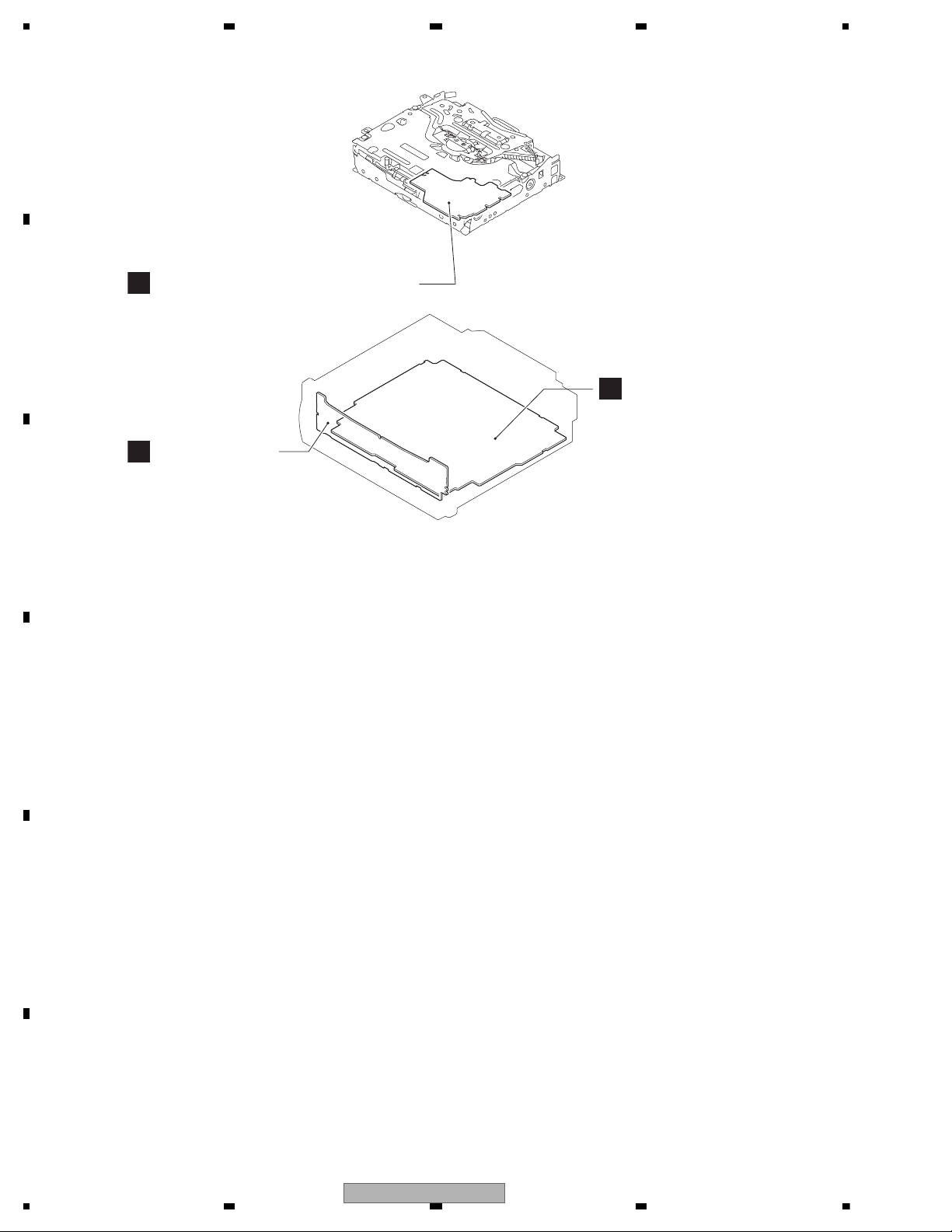
7. DISASSEMBLY
- Removing the Case (not shown)
1. Remove the Case.
- Removing the CD Mechanism Module (Fig.1)
Release the two latches and then remove the
1
Panel Assy.
CD Mechanism Module
2
Remove the four screws.
2
2
Disconnect the connector and then remove the
CD Mechanism Module.
2
1
2
1
Panel Assy
Fig.1
- Removing the Tuner Amp Assy (Fig.2)
Remove the two screws.
1
Remove the two screws.
2
Straighten the tabs at six locations
3
indicated and then remove the Tuner
Amp Assy.
1
1
2
3
3
3
3
2
3
3
28
DEH-5200SD/XNEW5
Tuner Amp Assy
Fig.2
Page 29

5 678
56
7
8
C
D
F
A
B
E
- Removing the Cover
1
3
Cover
Remove the three hooks.
1
1
1
Remove the hooks in order of figure
and then remove the cover.
Remove the hook.
2
Remove the hook.
3
2
DEH-5200SD/XNEW5
29
Page 30

1234
1234
C
D
F
A
B
E
1. Hold the Upper and Lower Frames at the specified parts (circled with broken blue lines in the photo below).
2. You can hold the tabs of the Lower Frame (circled with broken green lines in the photo below) if you do so only while lifting
the Mechanism Unit from the table. Keeping the Mechanism Unit lifted by holding these tabs with your fingers may result in
deformation.
3. Be careful NOT to hold the front part of the Upper Frame or the CRG Mechanism and NOT to insert foreign objects into
these mechanisms. Doing so may result in deformation.
Proper handling
Improper handling
How to Hold the Mechanism Unit
30
DEH-5200SD/XNEW5
Page 31

5 678
56
7
8
C
D
F
A
B
E
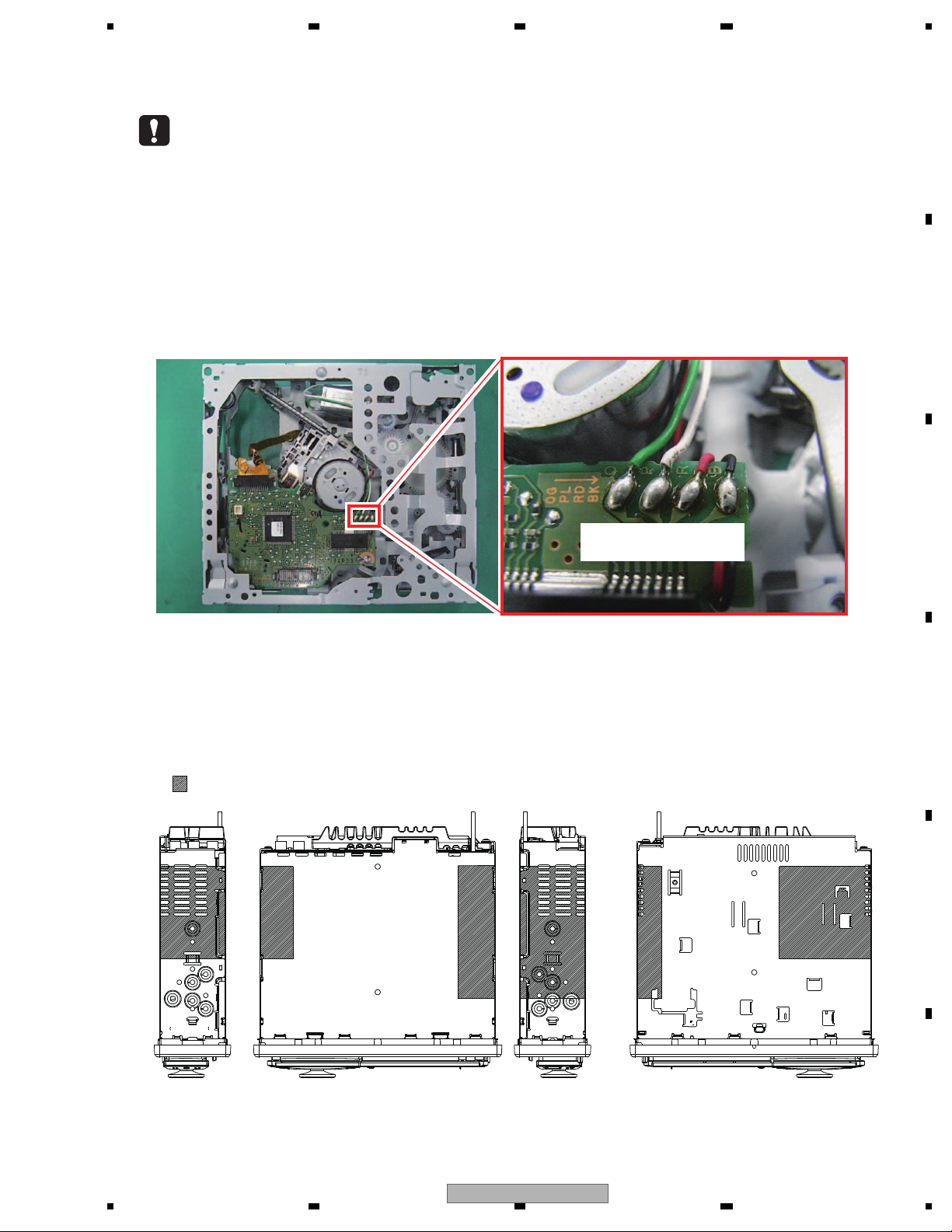
1. Remove the solder from the CRG-motor lead wire (Fig. 1).
2. Push in the Disc Detection Arm while applying 4-V power to the CRG Motor (Fig. 2). (Apply 4-V power to the green lead
wire. The white lead wire is for grounding.)
The Mechanism Module is set to the clamped state, and the PU will move toward the outer track.
Note: NEVER apply power to the CRG-motor lead wire without removing the solder from the wire. Doing so may result in
damage to the ICs and the PU.
3. Stop the motor when the PU reaches around the middle track.
Note: Jumpiness will occur when the PU reaches the outermost track. Although jumpiness does not constitute a problem,
it is recommended that it occur as least frequently as possible.
Fig. 1
Note: Be aware that the colors of the lead wires do not match the
indications on the Core Board Pattern (green wire to O and
white wire to P).
Fig. 2
Disc Detection Arm
Mechanism Module: How to Set to the Quasi-Clamp State (Driven by the Motor)
DEH-5200SD/XNEW5
31
Page 32

1234
1234
C
D
F
A
B
E
How to Remove the PU Unit
How to Move the PU toward the Outer Track
1. Set the unit to the quasi-clamp state, following the procedures described in “Mechanism Module: How to Set to the Quasi Clamp State (Driven by the Motor).”
2. Temporarily change the engagement position of the bias spring of the feed screw (Fig. 2b).
Be careful not to cut yourself on the tip of the spring.
3. Hold the PU unit by parts A in Fig. 1 then slide it toward the inner track.
4. Remove the backend of the feed screw from the outer holder, by first sliding it, as shown in Fig. 3, then lifting it.
5. Remove the PU unit, by lifting it. Lifting the PU unit will disengage the PU unit from the part B of the chassis.
Note: When reassembling the PU unit, be sure to securely engage the PU unit with the part B of the chassis, as shown in
Fig. 4. Also, be sure to change the engagement position of the bias spring of the feed screw to its original position
(Fig. 2a). After reassembling, perform the PU adjustment, following the description in the service manual.
1. Set the unit to the quasi-clamp state, following the procedures described in “Mechanism Module: How to Set to the Quasi Clamp State (Driven by the Motor).”
2. Move the PU unit toward the outer track, by applying 1.5-V power to the CRG motor.
Note: After moving the PU toward the outer track and taking the necessary measures, be sure to solder the lead wires.
Fig. 4
Fig. 3
Fig. 1
Fig. 2a
Original engagement
position
Fig. 2b
Temporary engagement
position
Slide toward the inner track.
One end of the spring is engaged
beneath the resin flange and
plate bend.
Outer holder
Backend of
the feed screw
Properly assembled state
[Improper assembly]
The chassis is not properly pinched by
the PU case and PU rack.
A
B
32
DEH-5200SD/XNEW5
Page 33

5 678
56
7
8
C
D
F
A
B
E
How to Remove the PU Rack
1. Remove the PU Unit, following the procedures described in “How to Remove the PU Unit.”
2. Remove the PU Rack fixing screw (Fig. 1).
3. Remove the PU Rack, by applying force in the direction of the arrow in Fig. 2.
Notes:
While handling the PU Unit, be careful NOT to touch the actuator block shown in Fig. 6 or bang the actuator block against
your workbench.
Handle the PU and PU Unit with care, according to the description in “How to Hold the PU.”
When reattaching the PU Rack to the PU, first reassemble parts a and b shown in Fig. 3 into the PU case then attach the
boss shown in Fig. 4 to the PU case.
After reassembling the PU Rack, insert the feed screw from side c in Fig. 5 (insertion depth: Approx. 18 mm for the part
indicated in the photo).
Fig. 1
Fig. 2
Fig. 3
Fig. 4
Fig. 5
Fig. 6
PU Rack
PU Rack
fixing screw
Actuator block
18 mm
b
c
a
DEH-5200SD/XNEW5
33
Page 34

1234
1234
C
D
F
A
B
E
How to Hold the PU
1. Be sure to hold the PU at the positions shown in “Proper handling.” NEVER hold it as shown in “Improper handling.”
Do not touch the object lens
and ACT.
Do not touch the VR.
Do not touch the Hologram.
Do not pull the FPC.
Proper handling Improper handling
34
DEH-5200SD/XNEW5
Page 35

5 678
56
7
8
C
D
F
A
B
E
1) Cautions on adjustments
In this product the single voltage (3.3 V) is used for the
regulator. The reference voltage is the REFO1 (1.65 V)
instead of the GND.
If you should mistakenly short the REFO1 with the GND
during adjustment, accurate voltage will not be obtained,
and the servo’s misoperation will apply excessive shock
to the pickup. To avoid such problems:
a. Do not mix up the REFO1 with the GND when
connecting the (-) probe of measuring instruments.
Especially on an oscilloscope, avoid connecting the (-)
probe for CH1 to the GND.
b. In many cases, measuring instruments have the same
potential as that for the (-) probe. Be sure to set the
measuring instruments to the floating state.
c. If you have mistakenly connected the REFO1 to the GND,
turn off the regulator or the power immediately.
Before mounting and removing filters or leads for
adjustment, be sure to turn off the regulator.
For stable circuit operation, keep the mechanism
operating for about one minute or more after the
regulator is turned on.
In the test mode, any software protections will not
work. Avoid applying any mechanical or electrical
shock to the mechanism during adjustment.
The RFAGC and RFO signals with a wide frequency range
are easy to oscillate. When observing the signals,
insert a resistor of 1k ohms in series.
The load and eject operation is not guarantied with the
mechanism upside down. If the mechanism is blocked
due to mistaken eject operation, reset the product or
turn off and on the ACC to restore it.
2) Test mode
This mode is used to adjust the CD mechanism module.
To enter the test mode.
[BAND] + [RDM] -> Reset
To exit from the test mode.
Turn off the ACC and back up.
Notes:
a. During ejection, do not press any other keys than the
EJECT key until the loaded disc is ejected.
b. If you have pressed the (→) key or (←) key during focus
search, turn off the power immediately to protect the
actuator from damage caused by the lens stuck.
c. For the TR jump modes except 100TR, the track jump
operation will continue even if the key is released.
d. For the CRG move and 100TR jump modes, the tracking
loop will be closed at the same time when the key is
released.
e. When the power is turned off and on, the jump mode
is reset to the single TR (91), the RF amp gain is set to 0 dB,
and the auto-adjustment values are reset to the default
settings.
When a CD-DA (regular music CD) is played in the CD
test mode, its sound quality will be temporarily
deteriorated. The CD will then repeat normal, deteriorated,
normal… playback.
This is due to the difference in the playback modes
between the normal operation mode and the CD test
mode, and the interval of generating deteriorated mode
and the time taken to return to the normal mode depend
on the error of each clock.
The time taken to turn to the deteriorated mode is at a
minimum around 20 seconds while the time to return to
the normal mode is maximum 40 seconds approximately.
Make sure to check the sound quality in the normal
operation mode.
8. EACH SETTING AND ADJUSTMENT
8.1 CD ADJUSTMENT
DEH-5200SD/XNEW5
35
Page 36

1234
1234
C
D
F
A
B
E
8.2 CHECKING THE GRATING AFTER CHANGING THE PICKUP UNIT
F
E
REFO1
CD CORE UNIT
Note :
The grating angle of the PU unit cannot be adjusted after the PU unit is changed. The PU unit in the CD mechanism
module is adjusted on the production line to match the CD mechanism module and is thus the best adjusted PU
unit for the CD mechanism module. Changing the PU unit is thus best considered as a last resort. However, if the
PU unit must be changed, the grating should be checked using the procedure below.
Purpose :
To check that the grating is within an acceptable range when the PU unit is changed.
Symptoms of Mal-adjustment :
If the grating is off by a large amount symptoms such as being unable to close tracking, being unable to perform
track search operations, or taking a long time for track searching.
Method :
Measuring Equipment
Measuring Points
Oscilloscope, Two L.P.F.
E, F, REFO1
Disc TCD-782
Mode TEST MODE
Checking Procedure
1. In test mode, load the disc and switch the 3 V regulator on.
2. Using the right and left buttons, move the PU unit to the innermost track.
3. Press key 3 to close focus, the display should read "91". Press key 2 to implement the tracking
balance adjustment the display should now read "81". Press key 3. The display will change,
returning to "81" on the fourth press.
4. As shown in the diagram above, monitor the LPF outputs using the oscilloscope and check that the phase
difference is within 75 . Refer to the photographs supplied to determine the phase angle.
5. If the phase difference is determined to be greater than 75 try changing the PU unit to see if there is any
improvement. If, after trying this a number of times, the grating angle does not become less than 75 then the
mechanism should be judged to be at fault.
Note
Because of eccentricity in the disc and a slight misalignment of the clamping center the grating waveform may be
seen to "wobble" ( the phase difference changes as the disc rotates). The angle specified above indicates the
average angle.
Hint
Reloading the disc changes the clamp position and may decrease the "wobble".
100 kohm
390 pF
100 kohm
390 pF
E
VREF
F
VREF
Xch Ych
L.P.F.
L.P.F.
Oscilloscope
36
DEH-5200SD/XNEW5
Page 37

5 678
56
7
8
C
D
F
A
B
E
Grating waveform
45 degrees
0 degrees
75 degrees
60 degrees
30 degrees
90 degrees
Ech -> Xch 20 mV/div, AC
Fch -> Ych 20 mV/div, AC
DEH-5200SD/XNEW5
37
Page 38

1234
1234
C
D
F
A
B
E
8.3 PCL OUTPUT CONFIRMATION
PCL output
In the normal operation mode (with the detachable panel installed, the ACC switched ON, the standby mode
cancelled), shift the TESTIN IC601(Pin 61) terminal to H.
The clock signal is output from the PCL terminal IC601(Pin 37).
The frequency of the clock signal is 625.0 kHz that is one 32th of the fundamental frequency.
The clock signal should be 625.0 kHz(- 10 Hz, + 15 Hz).
If the clock signal is out of the range, the X'tal (X601) should be replaced with new one.
38
DEH-5200SD/XNEW5
Page 39

5 678
56
7
8
C
D
F
A
B
E
DEH-5200SD/XNEW5
39
Page 40

1234
1234
C
D
F
A
B
E
9. EXPLODED VIEWS AND PARTS LIST
NOTES : Parts marked by " * " are generally unavailable because they are not in our Master Spare Parts List.
The > mark found on some component parts indicates the importance of the safety factor of the part.
Therefore, when replacing, be sure to use parts of identical designation.
Screw adjacent to mark on the product are used for disassembly.
For the applying amount of lubricants or glue, follow the instructions in this manual.
(In the case of no amount instructions,apply as you think it appropriate.)
""
5250SD/XNES
5250SD/XNES1
5290SD/XNID
5250SD/XNES
5250SD/XNES1
5290SD/XNID
5250SD/XNES
5250SD/XNES1
5290SD/XNID
5200SD/XNEW5
5200SD/XNEW5
5200SD/XNEW5
9.1 PACKING
40
DEH-5200SD/XNEW5
Page 41

5 678
56
7
8
C
D
F
A
B
E
(1) PACKING SECTION PARTS LIST
Mark No. Description Part No.
1 Cord Assy
2 Polyethylene Bag QEG3001
3Unit Box
4 Contain Box
5 Case Assy YXB5009
6 Accessory Assy
7Screw
8 Polyethylene Bag CEG1160
9 Handle CND3707
10 Screw Assy
* 11 Polyethylene Bag
12 Screw
See Contrast table (2)
See Contrast table (2)
See Contrast table (2)
See Contrast table (2)
See Contrast table (2)
See Contrast table (2)
See Contrast table (2)
See Contrast table (2)
Mark No. Description Part No.
13 Protector YHP5063
14 Protector YHP5064
15 Remote Control Unit
16 CD-ROM
* 17-1 Caution Card
* 17-2 Caution Card
* 17-3 Passport
* 17-4 Warranty Card
17-5 Quick Start GUI Manual
17-6 Installation Manual
* 17-7 Service Network
17-8 Operation Manual
See Contrast table (2)
See Contrast table (2)
See Contrast table (2)
See Contrast table (2)
See Contrast table (2)
See Contrast table (2)
See Contrast table (2)
See Contrast table (2)
See Contrast table (2)
See Contrast table (2)
(2) CONTRAST TABLE
DEH-5200SD/XNEW5, DEH-5250SD/XNES, DEH-5250SD/XNES1 and DEH-5290SD/XNID are constructed the
same except for the following:
Mark No. Description
1 Cord Assy CDP1268 CDP1269 CDP1269 CDP1269
3 Unit Box QHG3057 QHG3059 QHG3060 QHG3061
4 Contain Box QHL3057 QHL3059 QHL3060 QHL3061
6 Accessory Assy YEA5083 YEA5084 YEA5084 YEA5084
7 Screw BPZ20P060FTC Not Used Not Used Not Used
DEH-5200SD/XNEW5
DEH-5250SD/XNES
DEH-5250SD/XNES1
DEH-5290SD/XNID
10 Screw Assy Not Used YEA5082 YEA5082 YEA5082
* 11 Polyethylene Bag Not Used CEG-127 CEG-127 CEG-127
12 Screw Not Used TRZ50P080FTC TRZ50P080FTC TRZ50P080FTC
15 Remote Control Unit Not Used CXE2758 CXE2758 CXE2758
16 CD-ROM QPJ3003 Not Used Not Used Not Used
* 17-1 Caution Card CRP1389 Not Used Not Used Not Used
* 17-2 Caution Card CRP1394 Not Used Not Used Not Used
* 17-3 Passport CRY1268 Not Used Not Used Not Used
* 17-4 Warranty Card CRY1279 Not Used CRY1250 CRY1304
17-5
17-6 Installation Manual QRD3044 QRD3046 QRD3046 Not Used
* 17-7 Service Network Not Used Not Used CRY1251 CRY1305
17-8 Operation Manual Not Used QRD3045 QRD3045 QRB3046
Quick Start GUI Manual
QRD3042 Not Used Not Used Not Used
(Owner’s manual)
Owner's Manual,Installation Manual
Part No. Language
QRD3042 English, French, Italian, Spanish(Espanol), German, Dutch, Russian
QRD3044 English, French, Italian, Spanish(Espanol), German, Dutch, Russian
QRD3045 English, Spanish(Espanol), Portuguese(B), Arabic, Traditional Chinese
QRD3046 English, Spanish(Espanol), Portuguese(B), Arabic, Traditional Chinese
QRB3046 English
CONTENTS OF CD-ROM (Operation Manual), QPJ3003
Part No. Language
* QRB3032 English
* QRB3033 French
* QRB3034 Italian
* QRB3035 Spanish(Espanol)
* QRB3036 German
* QRB3037 Dutch
* QRB3038 Russian
* QRB3039 Swedish
* QRB3040 Norwegian
* QRB3041 Finnish
* QRB3042 Danish
* QRB3043 Portuguese
* QRB3044 Greek
* QRB3045 Turkish
All operation manuals are supplied in PDF files by the CD-ROM.
Regarding the availability of paper manual, contact Pioneer Service representative in your region.
DEH-5200SD/XNEW5
41
Page 42

1234
1234
C
D
F
A
B
E
9.2 EXTERIOR(1)
B
DEH-5250SD/XNES
DEH-5250SD/XNES1
DEH-5290SD/XNID
DEH-5250SD/XNES
DEH-5250SD/XNES1
DEH-5290SD/XNID
DEH-5200SD/XNEW5
42
DEH-5200SD/XNEW5
Page 43

5 678
56
7
8
C
D
F
A
B
E
(1) EXTERIOR(1) SECTION PARTS LIST
Mark No. Description Part No.
1 Cord Assy
2 Holder CND3598
3 Panel CNU1016
4 Detachable Assy
5 Screw BPZ20P100FTC
6 Button(DETACH) CAI2699
7 Button(TA[EW5], SW[ES, ES1, ID] ) CAI2700
8 Button(EJECT, CLK) CAI2701
9 Button(S.Rtrv, iPod, LOC) CAI2702
10 Spring CBH2210
11 Cover CNU1025
12 Lighting Conductor CNW1756
13 Knob Unit CXE2507
See Contrast table (2)
See Contrast table (2)
Mark No. Description Part No.
14 Spring XBL7005
15 Grille Unit
* 16 Door(USB) CAT2912
17 Button Unit(SRC, BAND, LIST, BACK) CXE2511
18 Holder CND5436
19 Double Side Tape CNM8673
20 Cushion CNN3211
21 Holder CNW1758
22 OEL Module MXS4011
23 Case YNB5063
24 Remote Control Unit
25 Cover
See Contrast table (2)
See Contrast table (2)
See Contrast table (2)
(2) CONTRAST TABLE
DEH-5200SD/XNEW5, DEH-5250SD/XNES, DEH-5250SD/XNES1 and DEH-5290SD/XNID are constructed the
same except for the following:
Mark No. Description
1 Cord Assy CDP1268 CDP1269 CDP1269 CDP1269
4 Detachable Assy QXA3213 QXA3214 QXA3214 QXA3216
15 Grille Unit CXE2895 CXE2897 CXE2897 CXE2896
24 Remote Control Unit Not Used CXE2758 CXE2758 CXE2758
25 Cover Not Used CNS7068 CNS7068 CNS7068
DEH-5200SD/XNEW5
DEH-5250SD/XNES
DEH-5250SD/XNES1
DEH-5290SD/XNID
DEH-5200SD/XNEW5
43
Page 44

1234
1234
C
D
F
A
B
E
9.3 EXTERIOR(2)
A
B
B
A
A
C
C
44
DEH-5200SD/XNEW5
Page 45

5 678
56
7
8
C
D
F
A
B
E
(1) EXTERIOR(2) SECTION PARTS LIST
Mark
Mark No. Description Part No.
1 Screw ASZ26P050FTC
2 Screw BSZ26P060FTC
3 Screw BSZ26P100FTC
4 Cable CDE9106
5 Chassis CNA3152
No. Description Part No.
16 Holder CND5417
17 Holder CND5423
18 FM/AM Tuner Unit(U401)
19 Holder CND4324
> 20 Fuse(10 A) YEK5001
See Contrast table (2)
6 Earth Plate CNC8915
7 Cushion CNM8890
8 Insulator CNN3145
9 CD Mechanism Module(S11) CXK5800
10 Tuner Amp Assy
11 Screw BPZ26P080FTC
12 Screw BSZ26P060FTC
13 Screw BSZ26P100FTC
14 Screw BSZ26P160FTC
15 Holder CND5410
See Contrast table (2)
21 Heat Sink YNR5139
22 Button CAC4836
23 Spring(Thin) CBH2961
24 Spring(Thick) CBH2962
25 Panel CNU1015
26 Arm CNV9312
27 Arm CNW1439
28 Spring YBH5012
29 Cover YNN5030
30 Holder YND5048
(2) CONTRAST TABLE
DEH-5200SD/XNEW5, DEH-5250SD/XNES, DEH-5250SD/XNES1 and DEH-5290SD/XNID are constructed the
same except for the following:
Mark No. Description
10 Tuner Amp Assy QWM3122 QWM3123 QWM3123 QWM3123
18
FM/AM Tuner Unit(U401)
DEH-5200SD/XNEW5
CWE2097 CWE2098 CWE2098 CWE2098
DEH-5250SD/XNES
DEH-5250SD/XNES1
DEH-5290SD/XNID
DEH-5200SD/XNEW5
45
Page 46

1234
1234
C
D
F
A
B
E
9.4 CD MECHANISM MODULE
A
C
D
C
A
B
B
C
D
(A)
: GEM1045
(B)
: GEM1038
(C)
: GEM1024
(D)
: GEM1043
(C)
(C)
(A)
(A)
(D)
(D)
(A)
(A)
(D)
(A)
(A)
(A)
(A)
(A)
(C)
(C)
(C)
(C)
(B)
(C)
(C)
46
DEH-5200SD/XNEW5
Page 47

5 678
56
7
8
C
D
F
A
B
E
CD MECHANISM MODULE SECTION PARTS LIST
Mark
Mark No. Description Part No.
1 Screw BMZ20P020FTC
No. Description Part No.
50 Damper CNW1198
2 Screw BSZ20P040FTC
3 Screw(M2 x 4) CBA1835
4 Washer CBF1038
5 Spring CBH3010
51 Arm CNW1726
52 Motor Unit(M2)(LOAD/CRG) CXC4026
53 Screw Unit CXC8894
54 Arm Assy CXC8896
6 Spring CBH2855
55 Washer CBF1037
7 Spring CBH2856
8 Spring CBH2860
9 •••••
10 Spring CBH3011
56 Washer CBF1038
57 Arm CND4554
58 Collar CNV6906
59 Roller CNW1196
11 Spring CBH3012
12 Spring CBH3014
13 Spring CBH3015
14 Spring CBH3016
15 Spring CBH3017
60 Gear Unit CXC8893
61 Washer YE15FTC
62 Chassis Unit(M1)(SPDL) CXE1946
63 Motor Unit CXE2273
64 Screw JFZ20P025FTC
16 Spring CBH3018
65 Screw JGZ17P022FTC
17 Spring CBH3019
18 Spring CBH3020
19 Spring CBL1797
66 Screw IMS20P030FTC
67 CD Core Unit (S11STD-DOUT) CWX3774
20 Pickup Unit(S10.5)(Service) CXX1942
21 Bracket CND4553
22 Arm CND4555
23 Frame CND4557
24 Frame CND5217
25 Lever CND5398
26 Sheet CNN2280
27 Rack CNV8342
28 Guide CNW1171
29 Roller CNW1172
30 Arm CNW1173
31 Arm CNW1174
32 Roller CNW1175
33 Lever CNW1176
34 Arm CNW1177
35 Arm CNW1178
36 Gear CNW1180
37 Gear CNW1181
38 Gear CNW1182
39 Gear CNW1183
40 Rack CNW1184
41 Gear CNW1185
42 Gear CNW1186
43 Gear CNW1187
44 Gear CNW1188
45 Clamper CNW1190
46 Arm CNW1192
47 Holder CNW1193
48 Holder CNW1194
49 Damper CNW1197
DEH-5200SD/XNEW5
47
Page 48

1234
1234
C
D
F
A
B
E
10. SCHEMATIC DIAGRAM
A-a A-b
A-a
A-b
A-b
A-a
Large size
SCH diagram
Guide page
Detailed page
Note: When ordering service parts, be sure to refer to " EXPLODED VIEWS AND PARTS LIST" or
"ELECTRICAL PARTS LIST".
1/2
A
A-a
1/2
SYNC Freq.
KEYAD
KEYD
PEE
IP_RX
IP_TX
ASENB0
DSENS
ASENS
PEE
SYNC
FLG
BSENS
KEYAD
SL
ROT1
ROT0
RWCNVSS
BUSR-
BUSR+
BUSL+
BUSL-
IP_RX
IP_TX
IPPW
BUSR-
BUSR+
BUSL-
LDET
CE2
SYNC
USBCTL
FLG
DI
CK
CE1
DO
KYDT
KYDT
BUSL+
ASENB0
DM
DP
ISENS
DPDT
DPDT
SYStoSH
SHtoSYS
FLPILM
VDCONT
USBCTL
DALMON
DALMON
AANT
RESET
RESET
VDD5V
KEYD
KEYD
RWCLK
RWCLK
SYSPW
SYSPW
RDSDT
SL
RCK
RDSLK
USB5V
TUNL
TUNR
AUXL
AUXR
AUXG
CDL
CDR
TUNR
TUNL
BUP
DD5V
SYS8V
RDS57K
BZ601
CPV1062-
1
1
2
2
CN801
CKS6188-
1
234
56789
10111213141516
17
181920
C161
220u/16
C165
0.01u/10
C164
470p/50
C163
0.1u/16
C162
1u/16
C152
0.1u/10
C151
0.1u/10
C201
1u/10
C202
1u/10
C604
12p/50
C101
0.1u/16
C605
10p/50
C204
NM
C102
NM
C206
NM
C103
NM
C606
0.1u/10
C203
1u/10
C610
0.1u/10
C104
NM
C403
NM
C205
NM
C209
0.22u/10
C211
NM
C210
NM
C401
0.01u/10
C607
NM
RB7
D161
CRG03
D601
RB551V-30
GND
GND
GND
GND
GND
GND
GND
GND
GND
GND
GND
GND
GND
GND
BD9781HFP
IC161
1
VIN
2
SW
3RT4
GND
5
FB
6
INV
7
EN
IC151
R5523N001B
EN
1
GND
2
FLG3VIN
4
5
VOUT
HA12241FP
IC101
DIN1
1
ROUT
2
DIN2
3
GND
4
5
BUS-
6
BUS+
7
VCC
8
STBY
JA661
CKS4124-
2
3
1
JA101
CKS5271-
1
2
3
4
5
6
7
8
9
10
11
M2R6TP_GND
KN401
L801
CTF1713-A
12
34
L602
NM
L151
NM
CTF1735-
L101
NM
L161
CTH1253-A
L402
BTH1101-A
L401
BTH1100-A
Q401
UMH1N
1
2
3
4
5
6
Q402
UMH1N
1
2
3
4
5
6
R409
22k
2
1
4
3
6
5
8
7
R802
2
R803
2
R805
2
R8121R811
1
R163
30k
R162
NM
R161
100kF
R151
100k
R101
62
R601
1k
R602
4.7k
R603
1M
R604
100
R605
100k
R606
2.2k
R607
100k
R609
100k
R610
100k
R103
100
R611
4.7k
R612
4.7k
R613
100k
R614
100k
R615
100k
R804
2
R104
100
R105
1k
R801
2
R168
470
1608
R106
2.2k
R662
1k
R401
680
R114
1k
R
R113
1k
R661
1k
R112
22k
R111
22k
R402
680
R403
680
R110
180
R407
680
R408
1.5k
R109
180
R406
680
R405
680
R404
680
R108
4.7k
R107
22k
KEYD2
MED_TX
MED_RX
PCL1
DPDT1
SYNC
USB5
KYDT1
USBCTL
FLG
BUSL2
BUSR2
BUSR1
ASENB1
BUSL1
BUS-
BUS+
TUNR
TUNL
BEGND
RHSLK
RLOCK
RDT
RCK
TUN3V
TUNG
D0
DI
CK
CE1
CE2
SL
TUN8V
RFGND
FMANT
RESET1
DGND
ROT1
ROT0
AUXL
AUXR
OEL+B
ILM+B
USBG
USBDP
USBDM
DPDT
VBUS
KYDT
DSENS
CNVSS
LDET
OSCG
VA812
NM
1
2345
6
VA804
VA662
NM
VA661
NM
VA805
VA806
VA808
X601
CSS1797-A
P401
IMSA-6802-01Y900
POWER_BUS
uCOM_BUS
GND
IC201
S1Q+R
1
S2A-R
2
S3A+R
3
S4B-R
4
5
S5B+R
6
S6R7MNR
8
MPR9SOR10INFR11INRR12INPR
13
OUTPR14OUTRR15OUTFR
26
OUTRL27OUTPL
28
INPL29INRL30INFL
31
SOL32MPL33MNL
34
S6L
35
S5B+L36S4B-L37S3A+L38S2A-L
39
S1Q+L
40
QCOM
C208
0.22u/10
C207
NM
GND
GND
GND
GND
LTC114EUB
Q102
LSA1576UB
Q101
C405
0.01u/10
C404
NM
GND
R203
NM
R204
NM
GND
D162
CRG03
C433
4.7u/10
GND
D432
NM
C431
4.7u/6.3
D431
NM
C432
0.01u/10
NJM2885DL1-33
IC431
1IN2
GND3OUT
AUXG
ILMG
R806
2
C801
NM
GND
R629
100k
GND
R608
NM
R619
4.7k
OELG
R167
1k
C166
150U/6.3
C167
470p/50
R164
NM
R165
100kD
R166
24kD
D163
CMS02
D164
NM
C219
1u/10
C220
NM
C221
1u/10
C218
NM
DALMON
IC
1
2
3
4
5
BYTE
6
CNVSS
7
8
9
RESET
10
XOUT
11
VSS1
12
XIN
13
VCC1
14
15
16
17
18
19
20
21
22
23
24
25
262728
29
30
31
323334
35
363738 88
89909192939495
VREF96AVCC
979899
100
VA807
CSENS
VA803
R810
2
R169
120
U401
1
AMANT
2
RFGND
3
FMANT
4
VCC
5
SL
6
CE2
7
NC1
8
CE1
9
CK
10
DI
11
LDET
12
OSCGND
13
ROM_VDD
14
DO
15
DGND
16
NC2
17
VDD_3.3
18
RDS_CK
19
RDS_DATA
20
RDS_LOCK
21
RDS_HSLK
22
AGND
23
Lch
24
Rch
L403
LCTAW220J2520-T
AMANT
L404
NM
C407
0.01u/10
C408
NM
R410
82k
R411
82k
C409
1500p/50
C410
1500p/50
GND
EJECT
FLPILM
IPGND
KEYAD
KEYD
D801
DZ2S068C
D802
DZ2S068C
C402
CCG1192-A
10u/10
C406
CCG1192-A
10u/10
C222
NM
C223
NM
R206
NM
R205
NM
GND
GND
M2R6TP_GND
KN801
JA401
CKX1070-
1
2
3
C802
0.01u/16
GND
C225
0.1u/10
R412
0
GND
GND
C227
NM
ILM
BUP
VDD3.3V
VDD5V
SYS8V
A
RF
EVOL
DGND
ILMG
SWVDD
AUX R
AUX L
AUX G
OEL+B
NC
DPDT
KYDT
USBDM
USBDP
ROT0
ROT1
DSENS
USBGND
SYS.
GRILLE
TUNER
DDCON
IPBUS
WIRE REMOTE
OELGND
ILM+B
VBUS
OEL
REFERENCE AREA MAP sheet1
101~120
151~160
161~170
201~240
241~250
301~350
IP-BUS
USB H.SW
DC-DC CONVERTOR
E.VOL
RCA
AMP
MUTE
TUNER
TUNER 3V REG
SYSTEM MICRO
ROM CORRECTOR
RESET
GRILLE
ILM+B
SWVDD
VDD5&VDD3.3
SYS+B
ASENS&BSENS
ISENS
B.REM
TEL MUTE
AUTO ANTENNA
SOURCE CONNECTOR
E.VOL VP+B
381~400
401~430
431~440
351~380
601~640
641~650
651~660
851~870 OEL+B
801~820
821~830
841~850
901~910
911~920
921~930
931~940
941~950
951~960
961~970
981~990
501~560
FLASH ROM
781~800
MECHA VD
ipod CP
MEDIA uCOM
DAC&LPF
561~580
MECHA
751~780
SDRAM
REFERENCE AREA MAP sheet2
581~590
591~600
181~200
491~500
701~750
SD
MED3.3V&MED1.2V
RF
X-2026
FM/AM TUNER UNIT
D
20.0MHz
ILM
USB
D
SIZE 1608
BUS+
BUS-
L-
R-
R+
L+
831~340 DSENS
871~880 FLPILM
661~670 WIRED REMOTE
*A
US
US
A
US
TUNER 3V REG
D
USBGND
SIZE 1608
ILM
ROT1
ROT0
NC
ISENS
NC
NC
ANTPW
NMI
BSENS
DSENS
ASENS
VDCONT
PEE
FLPILM
USBFLG
SYNC
RX2
NCRXTX
DPDT
KYDT
NC(RWCLK)
KEYD
MEDTX
MEDRX
USBCTL
PCL
ASENB0
DALMON
SYSPW
NCNCNC
NC
KEYAD
NC
SL
AVss
NC
NC
NC
NM
NM
*A
BUP
VDD5V
VDD3.3V
370.4kHz
416.6Hz
CWE2098-(B,C,D)
CWE2097-(A)
NM
NM
VA803-VA811
VR105C5R0AAA
SIZE 16
A
A
SIZE 1608
NM
NM
NM
FLASH MEMORY451~460
681~700
D
CCH1804-A-P25
*A
A
A:PEG64
B,C,D:PEG64
2/2
A
Symbol indicates a resistor.
No differentiation is made between chip resistors and
discrete resistors.
NOTE :
Symbol indicates a capacitor.
No differentiation is made between chip capacitors and
discrete capacitors.
B
CN1801
TUNER(EW5):-20.00 dBs
TUNER(OTHERS):-24.00 dBs
IP-BUS: +2.20 dBs
CD/USB/SD: +3.04 dBs
AUX: +2.20 dBs
IP-BUS:+2.20 dBs
TUNER(EW5):-20.00 dBs
TUNER(OTHERS):-24.00 dBs
(30%)
10.1 TUNER AMP ASSY(MAIN)(GUIDE PAGE)
DEH-5200SD/XNEW5
48
Page 49

5 678
56
7
8
C
D
F
A
B
E
1/2
A
A-b
1/2
VIN
VOUT
GND
CONTROL
TAB
PW-GND2
OUT2(-)
STBY
OUT2(+)
VCC2
OUT1(-)
PW-GND1
OUT1(+)
RIPPLE
IN1
IN2
IN3
AC-GND
OUT3(+)
PW-GND3
OUT3(-)
VCC1
OUT4(+)
MUTE
OUT4(-)
PW-GND4
PRE-GND
IN4
H-SW/
VDS-DET
TELIN
ISENS
BSENS
ASENS
DALMON
RL-
RL+
FL-
FL+
FR+
FR-
RR+
RR-
FR
RL
SWL
SWR
DPDT
RWCNVSS
RESET
KYDT
RWCLK
KEYD
SWVDD
MUTE
ILMPW
IP_RX
IP_TX
ASENB0
RESET
VST
VCK
VDT
IPPW
CE2
CE1
DI
RDSLK
KEYAD
SL
VDT
VCK
VST
RR
DPDT
SWL
SWR
FR
RR
RL
FL
LDET
RCK
ILMPW
OELPW
DALMON
KYDT
KYDT
SWR
FR
RR
SWL
RL
FL
RR-
RL-
RR+
RL+
FR-
FL-
FR+
FL+
MUTE
FL
SYSPW
FLPILM
KYDT
RDSDT
RDS57K
DPDT
SYStoSH
SHtoSYS
DIM
DIM
CSENS
EJTIN
TELIN
MEDRST
MEDSTBY
MEDMUTE
EJTIN
OELPW
SYSPW
SWVDD
DSENS
SYSPW
DALMON
DALMON
OELPW
KEYD
KEYD
RWCLK
RWCLK
SDCTL
CSENS
SYSPW
SYSPW
SYSPW
AANT
DO
AUXL
AUXG
AUXR
ROT0
CK
ROT1
DSENS
CCH1732-A
C361
3300u/16
100u/16
C913
C901
CCH1201-A
22u/16
C381
220u/10
C911
C961
0.1u/16
C242
NM
C962
0.047u/16
C932
NM
C931
1u/16
C921
0.1u/16
C214
0.1u/10
C951
0.1u/16
C851
CCG1111-A
C213
CCG1192-A
10u/10
C842
NM
C902
0.01u/10
C903NMC904
CCG1192-A
10u/10
C841
NM
C907
4.7u/6.3
C906
NM
C912
NM
C821
0.1u/16
C941
0.047u/16
C362
0.1u/16
C364
2.2u/10
C363
2.2u/10
C365
10u/35
CCG1236-A-T
C366
NM
2125
C854
330p/50
C853
0.01u/25
C351
0.47u/10
C352
0.47u/10
C353
0.47u/10
C354
0.47u/10
C311
NM
C367
CCG1192-A
10u/10
C312
NM
C309
NM
C310
NM
C307
NM
C308
NM
C603
4.7u/6.3
C602NMC601
CCG1192-A
10u/10
C855
0.1u/16
C905
4.7u/6.3
C609
NM
C608
0.1u/10
C858
0.1u/16
C651
1u/10
C641
NM
0.1u
C304
CCG1192-A
10u/10
C301
CCG1192-A
10u/10
C302
CCG1192-A
10u/10
C303
CCG1192-A
10u/10
C305
CCG1192-A
10u/10
C306
CCG1192-A
10u/10
D982
CRG03
D851
RB551V-30
D962
CRG03
D961
CRG03
D651
1SS352
D383
1SS352
D981
CRG03
D602
RB751S-40
D931
CRG03
D901
CRG03
D941
CRG03
D942
CRG03
D951
MC2848-11
D382
MC2848-11
D921
HZU7L(C2)
D922
HZU7L(A1)
D852
HZU10(B1)
D821
UDZS9R1(B)
D381
RKZ8.2KG(B2)
D902
UDZS5R6(B)
GND
GND
GND
GND
GND
GND
GND
GND
GND
GND
GND
GND
GND
GND
GND
GND
GND
GND
GND
GND
GND
GND
GND
GND
GND
GND
GND
GND
GND
GND
GND
GND
NJM2885DL1-33
IC901
1
IN
2
GND3OUT
IC651
S-80827CNNB-B8M
OUT
1
VDD
2
NC
3
VSS
4
NJM2360AM
IC851
CS
1
ES
2
CT
3
GND
45
INVIN
6
V+
7
SI
8
CD
NM
IC641
S-93C46ADFJ
CS
1
SK
2
DI
3
DO
45
GND
6
TEST
7
NC
8
VCC
IC961
TPD1018F
1
OUT
2
GND1
3
GND2
4
GND3
5
VDD
6IN7
GND48GND59GND610DIAG
NJM2388F84
IC911
123
4
IC351
PA2030A
1
2
3
4
5
6
7
8
9
10
11
12
15
16
17
18
19
20
21
22
23
24
25
13
14
JA301
1
2
3
4
5
6
7
8
9
10
L603
NM
L601
BTH1103-A
L841
NM
L951
BTH1101-A
L201
NM
L852
CTF1660-A
LTC114EUB
Q931
LTC114EUB
Q361
NM
Q362
RT3CLLM(EF)
Q921
123
456
RT3T22M
Q822
1
2
34
5
6
RT3T22M
Q902
1
2
34
5
6
RT3T22M
Q852
1
2
34
5
6
RT3T22M
Q382
1
2345
6
Q901
2SD2396(K)
Q851
2SD1760F5(R)
Q381
LSC4081UB(QRS)
Q821
2SD1767(R)
LSA1576UB
Q951
R201
1k
2
1
4
3
658
7
R802
2.2k
R803
2.2k
R805
2.2k
R815
100k
R813
100k
R814
22k
R355
R359
R842
4.7k
R351
R353
R360
R616
100k
R621
100k
R804
2.2k
R352
R822
1
R821
2.2k
R356
R853
NM
R854
1.3kF
R354
R801
2.2k
R312
22k
R309
22k
R310
22k
R856
1
R855
1k
R307
22k
R308
22k
R303
R858
180
(1/4W)
R305
82
R857
NM
R304
R651
100k
R652
1.5k
R306
82
R302
82
R851
NM
(3216)
R301
82
R641
NM
100k
R642
NM
1k
R643
100k
R622
NM
R623
100k
R385
1k
R365
10k
R383
47k
R382
100k
R384
47k
R626
10k
R381
47k
R358
R364
NM
R363
330
R362
10k
R361
10k
R911
47k
R903
22k
R901
680
R923
47k
R921
100k
R311
22k
R357
R852
15kF
R924
47k
R922
10k
R925
4.7k
R931
10k
R241
NM
R961
10k
R951
1k
R952
22k
R954
15k
R314
R617
100k
S652
CSG1020-
12
RESET
BUP2
MUTE1
MEDSTBY
MEDMUTE
KEYD2
EPM
MED_TX
MED_RX
PCL1
VDD33V
VDD5V
GND1
SWVDD
BSENS2 BSENS1
SYS+B
DT1
OEL9V
ASENS1
MUTE2
MUTE3
RR
RL
SWR
SWL
FR
FL
RCAG
TEST1
ILMB
BUP1
OEL15.5V
GND2
VA804
VA805
VA806
VA808
OEL+B
OEL+B
GND
GND
100u/16
C856
47u/25
C852
L851
NM
47u/25
C241
GND
R926
1k
(1/4w)
R932
1k
(1/4w)
C356
0.47u/16
PM9012A
S3A+R
S4B-R
4
5
S5B+R
6
S6R7MNR
8
MPR9SOR10INFR11INRR12INPR
13
OUTPR14OUTRR15OUTFR
16
GND
17
VREF18VCCL
19
FILH
20
VCCH
21
STB22CLK
23
DATA24DGND
25
OUTFL
26
OUTRL27OUTPL
28
INPL29INRL30INFL
31
SOL32MPL33MNL
34
S6L
35
S5B+L36S4B-L37S3A+L
S2A-L
C212
CCG1192-A
10u/10
JA981
CKM1586-
1
2
3
4
5
6
7
8
9
10
11
12
14
15
16
17
18
13
R313
BREM
ACC
A.ANT
ILL
TEL
RR-
RL-
RR+
RL+
FR-
FL-
FR+
FL+
C963
NM
R832
100k
R831
1kCSN1039-A
S831
12
GND
DSENS1
LTC114EUB
Q872
R871
1k
LSA1576UB
Q871
R873
10k
R872
47k
GND
GND
R322
4.7k
R843
47k
L242
NM
RT3C99M
Q301
1
2
34
5
6
R321
4.7k
RT3C99M
Q302
1
2
34
5
6
R319
4.7k
R320
4.7k
R318
4.7k
RT3C99M
Q303
1
2
3
4
5
6
GND
R902
680
R823
1.8k
VP+B
miniSMDC075F/24
P301
12
GND
R806
2.2k
C801
NM
GND
R627
100k
D822
UDZS7R5(B)
LTC114EUB
Q823
R628
4.7k
R620
100k
R618
100k
MEDRST
R912
1k
8VCONT
R619
4.7k
LSA1576UB
Q853
LTC114EUB
Q854
C859
1000p/50
R859
47k
R860
6.8k
R861
NM
P851
CEK1276-A
(250mA)
C355
0.47u/16
C358
0.47u/16
C357
0.47u/16
R816
22k
R817
22k
C219
1u/10
C220
NM
C221
1u/10
C218
NM
C215
CCG1192-A
10u/10
RT3T22M
Q351
1
2345
6
R366
10k
LSA1576UB
Q841
R844
1k
LTC114EUB
Q842
R841
NM
VA809
VA810
VA811
R807
100
R808
100
R809
100
D853
MC2848-11
R625
NM
CE
DALMON
IC601
272829
30
31
323334
35
36373839404142
4344454647
48
49
50
51
52
53
54
55
56
57
58
59
VCC2
60
61
VSS2
62
63
64
65
66
67
68
69
70
71
72
73
74
75
76777879808182838485868788899091929394
95
VREF96AVCC
979899
VA807
Q242
LSC4081UB(QRS)
RT3T22M
Q241
1
2
34
5
6
L241
NM
D241
UDZS15(B)
C243
0.22u/16
C244
NM
R242
1.8k
R862
0
GND
R863
1608
C359
NM
3216
NM
CN601
CKS5033-
1
2345678
9
10
L982
CTH1445-A
12
C822
1u/16
VA803
R810
2.2k
VDDIN
D801
DZ2S068C
D802
DZ2S068C
C611
NM
VDD3.3
GND
C222
NM
C223
NM
R206
NM
R205
NM
GND
GND
VDuP
R386
NM
TEST2
TEST3
S651
CSG1020-
12
R624
100k
C216
2.2u/16
C224
NM
C217
0.1u/16
100u/16
C226
C802
0.01u/16
GND
GND
C225
0.1u/10
R874
1.5k
C964
NM
GND
R317
4.7k
GND
GND
C227
NM
D
D
ILM
A
EVOL VP+B
EVOL
RCA OUT
AMP
MUTE
VDD3.3V
VDD5.0
OEL
A.ANT
TELMUTE
ISENS
BSENS&ASENS
SYS+B
RESET
ROM CORRECTION
NM
SYS. MICRO
ILM+B
SWVDD
OEL+B
B.REM
SOURCE
CONNECTOR
A
9.4V15.5V
BUP
8.4V(DIM OFF)
A
3.6k
5.6k
NM
B.UP
10 A
B.UP
GND
BREM
NC
ACC
A.ANT
ILL
TEL
RL-
FL-
RL+
FL+
RR-
FR-
RR+
FR+
ILM
RR
FL
FR
RL
105
SYS8V
VDD3.3V
VDD5V
BUP
DSENS
FLPILM
ILM
D
(1/10W)
freq.=72kHz
VDD3.3V
A
1500u/16
A
NM
A
A
A
A
A
SIZE 1608
SIZE 1608
ILM
ROT1
ROT0
NC
MEDRST
USBFLG
SYNC
RX2
NCRXTX
DPDT
KYDT
NC(RWCLK)
KEYD
MEDTX
MEDRX
EJTIN
PCL
ASENB0
WRBSY
TELIN
MEDSTBY
MEDMUTE
DALMON
SYSPW
SWVDD
MUTE
ILMPW
NC(CE)
OELPW
IPPW
VDT
VCK
VST
ROMDATA
ROMCK
ROMCS
NC
TESTIN
TUNPCE2
TUNPCE1
TUNPCK
TUNPDI
NC
NC
NC
TUNPDO
RCK
LDET
RDSLK
RDSDT
DIMMER
NC
SDCTL
NC
NCNCNCNCNCNCNC
NC
NC
NC
RDS57K
NC
CSENS
KEYAD
NC
SL
AVss
NC
NC
NC
NC
NC
NM
NM
14V
OEL
NM
6.8V(DIM ON)
VA803-VA811
VR105C5R0AAA-T
*A
ILM
SIZE 1608
A
A
YEK5001
NM
NM
NM
NM
NM
NM
D
NM
0
P/O:1 / 3
-- / RR
-- / RR
SWR/ SWR
-- / SWL
SWL/ FR
-- / FL
XKB7001-
3P/O:
RF
GND
GND
GND
GND
A
82
82
3.6k
3.6k
3.6k
5.6k
5.6k
5.6k
NM
A:PEG645A8(256k)
B,C,D:PEG647A8(256k)
>
>
The > mark found on some component parts indicates
the importance of the safety factor of the part.
Therefore, when replacing, be sure to use parts of
identical designation.
NM : No Mount
TUNER AMP ASSY(MAIN)
1/2
A
A:DEH-5200SD/XNEW5
B:DEH-5250SD/XNES
C:DEH-5250SD/XNES1
D:DEH-5290SD/XNID
TUNER(EW5):+23.69 dBs
TUNER(OTHERS):+19.70 dBs
IP-BUS:+35.82 dBs
CD/USB/SD:+35.66 dBs
AUX:+35.82 dBs
TUNER(EW5): +1.99 dBs
TUNER(OTHERS): -1.99 dBs
IP-BUS:+14.13 dBs
CD/USB/SD:+13.97 dBs
AUX:+14.13 dBs
TUNER(EW5): +2.00 dBs
TUNER(OTHERS): -2.00 dBs
IP-BUS:+14.20 dBs
CD/USB/SD:+14.04 dBs
AUX:+14.20 dBs
DEH-5200SD/XNEW5
49
Page 50

1234
1234
C
D
F
A
B
E
A-a A-b
A-b
1/2
TAB
PW-GND2
OUT2(-)
STBY
OUT2(+)
VCC2
OUT1(-)
PW-GND1
OUT1(+)
RIPPLE
IN1
IN2
IN3
AC-GND
OUT3(+)
PW-GND3
OUT3(-)
VCC1
OUT4(+)
MUTE
OUT4(-)
PW-GND4
PRE-GND
IN4
H-SW/
VDS-DET
RL-
RL+
FL-
FL+
FR+
FR-
RR+
RR-
FR
RL
SWL
SWR
VST
VCK
VDT
CE2
CE1
DI
RDSLK
VDT
VCK
VST
RR
SWL
SWR
FRRRRL
FL
LDET
RCK
SWR
FR
RR
SWL
RL
FL
MUTE
FL
SYSPW
RDSDT
RDS57K
CSENS
EJTIN
SYSPW
SDCTL
DO
CK
CCH1732-A
C361
3300u/16
22u/16
C381
C242
NM
C214
0.1u/10
C213
CCG1192-A
10u/10
C362
0.1u/16
C364
2.2u/10
C363
2.2u/10
C365
10u/35
CCG1236-A-T
C366
NM
2125
C351
0.47u/10
C352
0.47u/10
C353
0.47u/10
C354
0.47u/10
C311
NM
C367
CCG1192-A
10u/10
C312
NM
C309NMC310
NM
C307NMC308
NM
C603
4.7u/6.3
C602
NM
C601
CCG1192-A
10u/10
C609
NM
C608
0.1u/10
C641
NM
0.1u
C304
CCG1192-A
10u/10
C301
CCG1192-A
10u/10
C302
CCG1192-A
10u/10
C303
CCG1192-A
10u/10
C305
CCG1192-A
10u/10
C306
CCG1192-A
10u/10
D383
1SS352
D602
RB751S-40
D941
CRG03
D382
MC2848-11
D381
RKZ8.2KG(B2)
GND
GND
GND
GND
GND
GND
GND
GND
GND
GND
GND
GND
GND
NM
IC641
S-93C46ADFJ
CS1SK2DI3DO
45
GND
6
TEST
7NC8
VCC
IC351
PA2030A
123456789
101112
1516171819202122232425
13
14
JA301
123456789
10
L603
NM
L601
BTH1103-A
L201
NM
LTC114EUB
Q361
NM
Q362
RT3T22M
Q382
1234
5
6
Q381
LSC4081UB(QRS)
R201
1k
2
1
4
3
6
5
8
7
R355
R359
R351
R353
R360
R352
R356
R354
R312
22k
R309
22k
R310
22k
R307
22k
R308
22k
R303
R305
82
R304
R306
82
R302
82
R301
82
R641
NM
100k
R642
NM
1k
R643
100k
R622
NM
R623
100k
R385
1k
R365
10k
R383
47k
R382
100k
R384
47k
R626
10k
R381
47k
R358
R364
NM
R363
330
R362
10k
R361
10k
R311
22k
R357
R241
NM
R314
MUTE1
1
MUTE2
MUTE3
RR
RL
SWR
SWL
FR
FL
RCAG
TEST1
OEL+B
GND
47u/25
C241
GND
C356
0.47u/16
PM9012A
OUTPR
14
OUTRR
15
OUTFR
16
GND
17
VREF
18
VCCL
19
FILH
20
VCCH
21
STB
22
CLK
23
DATA
24
DGND
25
OUTFL
26
OUTRL
27
OUTPL
INPL
C212
CCG1192-A
10u/10
R313
R322
4.7k
L242
NM
RT3C99M
Q301
1234
5
6
R321
4.7k
RT3C99M
Q302
1234
5
6
R319
4.7k
R320
4.7k
R318
4.7k
RT3C99M
Q303
123
456
GND
VP+B
miniSMDC075F/24
P301
12
R627
100k
R628
4.7k
C355
0.47u/16
C358
0.47u/16
C357
0.47u/16
C215
CCG1192-A
10u/10
RT3T22M
Q351
1234
5
6
R366
10k
IC601
37
38
39
40
41
42
43
44
45
46
47
48
49
50
515253545556575859
VCC2
60
61
VSS2
62636465666768697071727374
75
76
77
78
79
80
81
82
83
84
85
86
87
88
89
Q242
LSC4081UB(QRS)
RT3T22M
Q241
1234
5
6
L241
NM
D241
UDZS15(B)
C243
0.22u/16
C244
NM
R242
1.8k
C359
NM
3216
C611
NM
VDuP
R386
NM
TEST2
TEST3 R624
100k
C216
2.2u/16
C224
NM
C217
0.1u/16
100u/16
C226
C225
0.1u/10
C964
NM
GND
R317
4.7k
A
EVOL VP+B
RCA OUT
AMP
MUTE
VDD5.0
ROM CORRECTION
NM
B.REM
A
A
3.6k
5.6k
NM
RRFLFR
RL
105
VDD3.3V
A
A
A
A
A
A
A
SIZE 1608
MEDRST
EJTIN
PCL
ASENB0
WRBSY
TELIN
MEDSTBY
MEDMUTE
SYSPW
SWVDD
MUTE
ILMPW
NC(CE)
OELPW
IPPW
VDT
VCK
VST
ROMDATA
ROMCK
ROMCS
NC
TESTIN
TUNPCE2
TUNPCE1
TUNPCK
TUNPDI
NC
NC
NC
TUNPDO
RCK
LDET
RDSLK
RDSDT
DIMMER
NC
SDCTL
NC
NC
NC
NC
NC
NC
NC
NC
NC
NC
RDS57K
NC
CSENSNC
NC
NM
NM
14V
NM
0
P/O:1 / 3
-- / RR
-- / RR
SWR/ SWR
-- / SWL
SWL/ FR
-- / FL
XKB7001-
3P/O:
RF
GND
GND
GND
GND
82
82
3.6k
3.6k
3.6k
5.6k
5.6k
5.6k
NM
>
TUNER AMP ASSY(MAIN)
1/2
A
A:DEH-5200SD/XNEW5
B:DEH-5250SD/XNES
C:DEH-5250SD/XNES1
D:DEH-5290SD/XNID
TUNER(EW5): +1.99 dBs
TUNER(OTHERS): -1.99 dBs
IP-BUS:+14.13 dBs
CD/USB/SD:+13.97 dBs
AUX:+14.13 dBs
TUNER(EW5): +2.00 dBs
TUNER(OTHERS): -2.00 dBs
IP-BUS:+14.20 dBs
CD/USB/SD:+14.04 dBs
AUX:+14.20 dBs
50
DEH-5200SD/XNEW5
Page 51

5 678
56
7
8
C
D
F
A
B
E
A-a A-b
A-b
1/2
VIN
VOUT
GND
CONTROL
MUTE
OUT4(-)
PW-GND4
H-SW/
VDS-DET
TELIN
ISENS
BSENS
ASENS
DALMON
RR-
DPDT
RWCNVSS
RESET
KYDT
RWCLK
KEYD
SWVDD
MUTE
ILMPW
ASENB0
RESET
VST
VCK
VDT
IPPW
DPDT
ILMPW
OELPW
DALMON
RR-
RL-
RR+
RL+
FR-
FL-
FR+
FL+
MUTE
FLPILM
KYDT
DIM
DIM
TELIN
MEDRST
MEDSTBY
MEDMUTE
EJTIN
OELPW
SWVDD
DSENS
SYSPW
DALMON
OELPW
CSENS
SYSPW
SYSPW
AANT
AUXL
AUXG
AUXR
ROT0
ROT1
DSENS
CCH1732-A
C361
3300u/16
100u/16
C913
C901
CCH1201-A
220u/10
C911
C961
0.1u/16
C962
0.047u/16
C932
NM
C931
1u/16
C921
0.1u/16
C951
0.1u/16
C851
CCG1111-A
C842
NM
C902
0.01u/10
C903
NM
C904
CCG1192-A
10u/10
C841
NM
C907
4.7u/6.3
C906
NM
C912
NM
C821
0.1u/16
C941
0.047u/16
C854
330p/50
C853
0.01u/25
C367
CCG1192-A
10u/10
C855
0.1u/16
C905
4.7u/6.3
C858
0.1u/16
C651
1u/10
C641
NM
0.1u
D982
CRG03
D851
RB551V-30
D962
CRG03
D961
CRG03
D651
1SS352
D981
CRG03
D931
CRG03
D901
CRG03
D941
CRG03
D942
CRG03
D951
MC2848-11
D382
MC2848-11
D921
HZU7L(C2)
D922
HZU7L(A1)
D852
HZU10(B1)
D821
UDZS9R1(B)
D381
RKZ8.2KG(B2)
D902
UDZS5R6(B)
GND
GND
GND
GND
GND
GND
GND
GND
GND
GND
GND
GND
GND
GND
GND
GND
GND
GND
GND
GND
GND
GND
GND
NJM2885DL1-33
IC901
1
IN
2
GND
3
OUT
IC651
S-80827CNNB-B8M
OUT
1
VDD
2
NC
3
VSS
4
NJM2360AM
IC851
CS1ES2CT3GND
45
INVIN
6V+7SI8
CD
S-93C46ADFJ
CS
SK2DI3DO
45
GND
6
TEST
7
NC
VCC
IC961
TPD1018F
1
OUT
2
GND1
3
GND2
4
GND3
5
VDD6IN
7
GND4
8
GND5
9
GND6
10
DIAG
NJM2388F84
IC911
1
2
3
4
222324
25
L841
NM
L951
BTH1101-A
L852
CTF1660-A
LTC114EUB
Q931
LTC114EUB
Q361
NM
Q362
RT3CLLM(EF)
Q921
1
2
34
5
6
RT3T22M
Q822
1234
5
6
RT3T22M
Q902
1234
5
6
RT3T22M
Q852
1234
5
6
Q901
2SD2396(K)
Q851
2SD1760F5(R)
Q381
LSC4081UB(QRS)
Q821
2SD1767(R)
LSA1576UB
Q951
2.2k
2.2k
2.2k
R815
100k
R813
100k
R814
22k
R842
4.7k
R616
100k
R621
100k
2.2k
R822
1
R821
2.2k
R853NMR854
1.3kF
2.2k
R856
1
R855
1k
R858
180
(1/4W)
R857
NM
R651
100k
R652
1.5k
R851
NM
(3216)
R641
NM
100k
R642
NM
1k
R383
47k
R382
100k
R381
47k
NM330
R362
10k
10k
R911
47k
R903
22k
R901
680
R923
47k
R921
100k
R852
15kF
R924
47k
R922
10k
R925
4.7k
R931
10k
R961
10k
R951
1k
R952
22k
R954
15k
R617
100k
S652
CSG1020-
1 2
RESET
BUP2
MUTE1
MEDSTBY
MEDMUTE
EPM
PCL1
VDD33V
VDD5V
GND1
SWVDD
BSENS2 BSENS1
SYS+B
OEL9V
ASENS1
MUTE2
ILMB
BUP1
OEL15.5V
GND2
OEL+B
GND
100u/16
C856
47u/25
C852
L851
NM
R926
1k
(1/4w)
R932
1k
(1/4w)
JA981
CKM1586-
123456789
101112
1415161718
13
BREM
ACC
A.ANT
ILL
TEL
RR-
RL-
RR+
RL+
FR-
FL-
FR+
FL+
C963
NM
R832
100k
R831
1kCSN1039-A
S831
12
GND
DSENS1
LTC114EUB
Q872
R871
1k
LSA1576UB
Q871
R873
10k
R872
47k
GND
GND
R843
47k
R902
680
R823
1.8k
GND
2.2k
D822
UDZS7R5(B)
LTC114EUB
Q823
R620
100k
R618
100k
MEDRST
R912
1k
8VCONT
LSA1576UB
Q853
LTC114EUB
Q854
C859
1000p/50
R859
47k
R860
6.8k
R861
NM
P851
CEK1276-A
(250mA)
R816
22k
R817
22k
LSA1576UB
Q841
R844
1k
LTC114EUB
Q842
R841
NM
VA809
VA810
VA811
R807
100
R808
100
R809
100
D853
MC2848-11
R625
NM
CE
37
38
39
40
41
42
43
44
45
46
47
48
49
50
51525354555657
R862
0
GND
R863
1608
NM
CN601
CKS5033-
1
2
3
4
5
6
7
8
9
10
L982
CTH1445-A
12
C822
1u/16
0
2.2k
VDDIN
VDD3.3
GND
S651
CSG1020-
12
C802
GND
R874
1.5k
D
D
VDD3.3V
VDD5.0
OEL
A.ANT
TELMUTE
ISENS
BSENS&ASENS
SYS+B
RESET
ROM CORRECTION
ILM+B
SWVDD
OEL+B
B.REM
SOURCE
CONNECTOR
9.4V15.5V
BUP
8.4V(DIM OFF)
B.UP
10 A
B.UP
GND
BREMNCACC
A.ANT
ILL
TEL
RL-
FL-
RL+
FL+
RR-
FR-
RR+
FR+
ILM
105
SYS8V
VDD3.3V
VDD5V
BUP
DSENS
FLPILM
ILM
D
(1/10W)
freq.=72kHz
1500u/16
NM
A
A
MEDRST
PCL
ASENB0
WRBSY
TELIN
MEDSTBY
MEDMUTE
SYSPW
SWVDD
MUTE
ILMPW
NC(CE)
OELPW
IPPW
VDT
VCK
VST
ROMDATA
ROMCK
ROMCS
DIMMER
NC
NC
OEL
NM
6.8V(DIM ON)
*A
ILM
SIZE 1608
YEK5001
NM
NM
NM
NM
>
The > mark found on some component parts indicates
the importance of the safety factor of the part.
Therefore, when replacing, be sure to use parts of
identical designation.
NM : No Mount
TUNER(EW5):+23.69 dBs
TUNER(OTHERS):+19.70 dBs
IP-BUS:+35.82 dBs
CD/USB/SD:+35.66 dBs
AUX:+35.82 dBs
DEH-5200SD/XNEW5
51
Page 52

1234
1234
C
D
F
A
B
E
A-bA-a
A-a
1/2
A-b
1/2
SYNC Freq.
KEYAD
KEYD
PEE
DSENS
ASENS
PEE
BSENS
KEYAD
SL
ROT1
ROT0
RWCNVSS
BUSR-
BUSR+
BUSL+
BUSL-
IP_RX
IP_TX
IPPW
BUSR-
BUSR+
BUSL-
SYNC
USBCTL
FLG
BUSL+
ASENB0
ISENS
FLPILM
VDCONT
CSENS
AANT
RESET
RESET
VDD5V
USB5V
AUXL
AUXR
AUXG
CDL
CDR
TUNR
TUNL
BUP
DD5V
SYS8V
BZ601
CPV1062-
112
2
C161
220u/16
C165
0.01u/10
C164
470p/50
C163
0.1u/16
C214
0.1u/10
C162
1u/16
C152
0.1u/10
C151
0.1u/10
C213
CCG1192-A
10u/10
C201
1u/10
C202
1u/10
C604
12p/50
C101
0.1u/16
C605
10p/50
C204
NM
C102
NM
C206
NM
C103
NM
C606
0.1u/10
C203
1u/10
C610
0.1u/10
C104
NM
C205
NM
C209
0.22u/10
C211
NM
C210
NM
607
NM
D602
RB751S-40
D161
CRG03
GND
GND
GND
GND
GND
GND
GND
GND
BD9781HFP
IC161
1
VIN
2
SW
3
RT
4
GND
5
FB
6
INV
7
EN
IC151
R5523N001B
EN
1
GND2FLG
3
VIN
4
5
VOUT
HA12241FP
IC101
DIN11ROUT2DIN2
3
GND
4
5
BUS-6BUS+7VCC8STBY
JA661
CKS4124-
2
3
1
JA101
CKS5271-
1234567
8
9
10
11
L602
NM
L151
NM
CTF1735-
L101
NM
L161
CTH1253-A
R163
30k
R162
NM
R161
100kF
R151
100k
R101
62
R601
1k
R602
4.7k
R603
1M
R604
100
R605
100k
R606
2.2k
100k
100k
100k
R103
100
R104
100
R105
1k
R168
470
1608
R106
2.2k
R662
1k
R114
1k
R626
10k
R113
1k
R661
1k
R112
22k
R111
22k
R110
180
R109
180
R108
4.7k
R107
22k
TX
RX
1
SYNC
USB5
USBCTL
FLG
BUSL2
BUSR2
BUSR1
ASENB1
BUSL1
BUS-
BUS+
RESET1
CNVSS
VA662
NM
VA661
NM
X601
CSS1797-A
POWER_BUS
uCOM_BUS
IC201
PM9012A
S1Q+R
1
S2A-R
2
S3A+R
3
S4B-R
4
5
S5B+R
6
S6R
7
MNR
8
MPR
9
SOR
10
INFR
11
INRR
12
INPR
13
OUTPR
14
OUTRR
15
OUTFR
16
GND
17
VREF
18
VCCL
19
FILH
20
VCCH
21
STB
22
CLK
23
DATA
24
DGND
25
OUTFL
26
OUTRL
27
OUTPL
28
INPL
29
INRL
30
INFL
31
SOL
32
MPL
33
MNL
34
S6L
35
S5B+L
36
S4B-L
37
S3A+L
38
S2A-L
39
S1Q+L
40
QCOM
C208
0.22u/10
C212
CCG1192-A
10u/10
C207
NM
LTC114EUB
Q102
LSA1576UB
Q101
GND
R203NMR204
NM
GND
D162
CRG03
R629
100k
R627
100k
NM
R167
1k
C166
150U/6.3
C167
470p/50
R164NMR165
100kD
R166
24kD
D163
CMS02
D164
NM
C219
1u/10
C220
NM
C221
1u/10
C218
NM
IC601
12345
BYTE6CNVSS
789
RESET
10
XOUT11VSS112XIN13VCC1
1415161718192021222324
25
26
27
28
29
30
31
32
33
34
35
36
37
38
39
40
41
42
43
44
45
81
82
83
84
85
86
87
88
89
90
91
92
93
94
95
VREF
96
AVCC
97
98
99
100
R169
120
IPGND
KEYAD
KEYD
C222
NM
C223
NM
R206
NM
R205
NM
GND
GND
C224
NM
C225
0.1u/10
GND
GND
C227
NM
EVOL
SYS. MICRO
DDCON
IPBUS
WIRE REMOTE
20.0MHz
SIZE 1608
BUS+
BUS-
L-R-R+
L+
US
US
A
A
ROT1
ROT0
NC
ISENS
NC
NC
ANTPW
NMI
BSENS
DSENS
ASENS
VDCONT
PEE
MEDRST
FLPILM
USBFLG
SYNC
RX2
NC
RX
TX
DPDT
KYDT
NC(RWCLK)
KEYD
MEDTX
MEDRX
USBCTL
PCL
ASENB0
WRBSY
TELIN
MEDSTBY
MEDMUTE
DALMON
SYSPW
NC(CE)
NC
NC
NC
NC
NC
NC
NC
NC
NC
NC
KEYAD
NC
SL
AVss
NC
NC
NC
NM
NM
BUP
VDD5V
370.4kHz
416.6Hz
NM
A
A
NM
CCH1804-A-P25
A
A:PEG645B8(256k)
B,C,D:PEG647A8(256k)
2/2
A
TUNER(EW5):-20.00 dBs
TUNER(OTHERS):-24.00 dBs
IP-BUS: +2.20 dBs
CD/USB/SD: +3.04 dBs
AUX: +2.20 dBs
IP-BUS:+2.20 dBs
52
DEH-5200SD/XNEW5
Page 53

5 678
56
7
8
C
D
F
A
B
E
A-bA-a
A-a
1/2
A-b
1/2
IP_RX
IP_TX
ASENB0
ASENS
PEE
SYNC
FLG
LDET
CE2
USBCTL
FLG
DI
CK
CE1
DO
DPDT
KYDT
KYDT
DM
DP
DPDT
DPDT
SYStoSH
SHtoSYS
FLPILM
VDCONT
TELIN
MEDRST
MEDSTBY
MEDMUTE
USBCTL
DALMON
DALMON
KEYD
KEYD
RWCLK
RWCLK
SYSPW
SYSPW
RDSDT
SL
RCK
RDSLK
USB5V
TUNL
TUNR
AUXL
AUXG
AUXR
RDS57K
CN801
CKS6188-
1
2
3
4
5
6
7
8
9
10
11
12
13
14
15
16
17
18
19
20
C152
0.1u/10
C151
0.1u/10
C403
NM
C401
0.01u/10
C607
NM
D601
RB551V-30
GND
GND
GND
GND
GND
GND
GND
GND
GND
IC151
R5523N001B
EN
1
GND2FLG
3
VIN
4
5
VOUT
M2R6TP_GND
KN401
L801
CTF1713-A
12
34
L151
NM
CTF1735-
L402
BTH1101-A
L401
BTH1100-A
Q401
UMH1N
1
2
3
4
5
6
Q402
UMH1N
1
2
3
4
5
6
R409
22k
214
3
658
7
R802
2.2k
R803
2.2k
R805
2.2k
R812
1
R811
1
R151
100k
R606
2.2k
R607
100k
R609
100k
R610
100k
R611
4.7k
R612
4.7k
R613
100k
R614
100k
R615
100k
R616
100k
R804
2.2k
R801
2.2k
R401
680
R402
680
R403
680
R407
680
R408
1.5k
R406
680
R405
680
R404
680
MEDSTBY
MEDMUTE
KEYD2
EPM
MED_TX
MED_RX
PCL1
DPDT1
KYDT1
USBCTL
FLG
TUNR
TUNL
BEGND
RHSLK
RLOCK
RDT
RCK
TUN3V
TUNG
D0
DI
CK
CE1
CE2
SL
TUN8V
RFGND
FMANT
DGND
ROT1
ROT0
AUXL
AUXR
OEL+B
ILM+B
USBG
USBDP
USBDM
DPDT
VBUS
KYDT
DSENS
LDET
OSCG
VA812
NM
1234
5
6
VA804
VA805
VA806
VA808
P401
IMSA-6802-01Y900
GND
GND
GND
GND
GND
C405
0.01u/10
C404
NM
C433
4.7u/10
GND
D432
NM
C431
4.7u/6.3
D431
NM
C432
0.01u/10
NJM2885DL1-33
IC431
1
IN
2
GND
3
OUT
AUXG
ILMG
R806
2.2k
C801
NM
GND
GND
R608
NM
MEDRST
R619
4.7k
OELG
R
2
R816
22k
R817
22k
VA809
VA810
VA811
R807
100
R808
R809
100
DALMON
19202122232425
26
27
28
29
30
31
32
33
34
35
36
37
38
39
40
41
42
43
44
45
VA807
CSENS
VA803
R810
2.2k
R169
120
U401
1
AMANT
2
RFGND3FMANT
4
VCC
5SL6
CE27NC18CE1
9
CK10DI
11
LDET
12
OSCGND
13
ROM_VDD
14DO15
DGND
16
NC2
17
VDD_3.3
18
RDS_CK
19
RDS_DATA
20
RDS_LOCK
21
RDS_HSLK
22
AGND
23
Lch24Rch
L403
LCTAW220J2520-T
AMANT
L404
NM
C407
0.01u/10
C408
NM
R410
82k
R411
82k
C409
1500p/50
C410
1500p/50
GND
EJECT
FLPILM
D801
DZ2S068C
D802
DZ2S068C
C402
CCG1192-A
10u/10
C406
CCG1192-A
10u/10
GND
M2R6TP_GND
KN801
JA401
CKX1070-
1
2
3
C802
0.01u/16
GND
GND
R412
0
ILM
BUP
VDD3.3V
VDD5V
SYS8V
A
RF
DGND
ILMG
SWVDD
AUX R
AUX L
AUX G
OEL+B
NC
DPDT
KYDT
USBDM
USBDP
ROT0
ROT1
DSENS
USBGND
GRILLE
TUNER
OELGND
ILM+B
VBUS
OEL
REFERENCE AREA MAP sheet1
101~120
151~160
161~170
201~240
241~250
301~350
IP-BUS
USB H.SW
DC-DC CONVERTOR
E.VOL
RCA
AMP
MUTE
TUNER
TUNER 3V REG
SYSTEM MICRO
ROM CORRECTOR
RESET
GRILLE
ILM+B
SWVDD
VDD5&VDD3.3
SYS+B
ASENS&BSENS
ISENS
B.REM
TEL MUTE
AUTO ANTENNA
SOURCE CONNECTOR
E.VOL VP+B
381~400
401~430
431~440
351~380
601~640
641~650
651~660
851~870 OEL+B
801~820
821~830
841~850
901~910
911~920
921~930
931~940
941~950
951~960
961~970
981~990
501~560
FLASH ROM
781~800
MECHA VD
ipod CP
MEDIA uCOM
DAC&LPF
561~580
MECHA
751~780
SDRAM
REFERENCE AREA MAP sheet2
581~590
591~600
181~200
491~500
701~750
SD
MED3.3V&MED1.2V
RF
X-2026
FM/AM TUNER UNIT
D
ILM
USB
D
831~340 DSENS
871~880 FLPILM
661~670 WIRED REMOTE
*A
US
US
TUNER 3V REG
D
USBGND
SIZE 1608
ILM
ASENS
VDCONT
PEE
MEDRST
FLPILM
USBFLG
SYNC
RX2
NC
RX
TX
DPDT
KYDT
NC(RWCLK)
KEYD
MEDTX
MEDRX
USBCTL
PCL
ASENB0
WRBSY
TELIN
MEDSTBY
MEDMUTE
DALMON
SYSPW
NC(CE)
NM
*A
VDD3.3V
CWE2098-(B,C,D)
CWE2097-(A)
NM
VA803-VA811
VR105C5R0AAA-T
ILM
SIZE 1608
SIZE 1608
NM
NM
FLASH MEMORY451~460
681~700
D
*A
Symbol indicates a resistor.
No differentiation is made between chip resistors and
discrete resistors.
NOTE :
Symbol indicates a capacitor.
No differentiation is made between chip capacitors and
discrete capacitors.
B
CN1801
TUNER(EW5):-20.00 dBs
TUNER(OTHERS):-24.00 dBs
(30%)
DEH-5200SD/XNEW5
53
Page 54

1234
1234
C
D
F
A
B
E
10.2 TUNER AMP ASSY(MEDIA uCOM)(GUIDE PAGE)
2/2
A
A-a
2/2
CPPWR
CP_SCL
CP_SDA
CPRST
VDSENS
DACMUTE
DEEMPH
SD_DATA2
SD_CMD
SD_DATA3
SD_CLK
SD_DATA0
SD_DATA1
SD_WP
SD_CD
CDRST
CPRST
CPPWR
CDSRQ
CDSTBY
DACCLK
RAS
CAS
RD/WR
CKE
A16
A15
A14
A13
A12
A11
A10
A9
A20
WEO/DQML
A19
A18
A8
A7
A6
A5
A4
A3
A2
A2
A1
A14
A13
WEO/DQML
RD/WR
CAS
RAS
SDCS
PD7
A12
A10
A9
A8
A7
A6
A5
CKE
PD14
PD15
PD13
PD12
PD11
PD10
PD9
PD8
A11
A3
A4
PD0
PD1
PD2
PD3
PD4
PD5
PD6
CDSKIP
CDWAIT
CP_SCL
CP_SDA
CD_SDA
CD_SCL
A3A4A5A6A7A8A9
A10
A11
A12
A13
A14
A15
A16
A17
A18
BUP
SD_DATA1
SD_DATA0
SD_CMD
SD_DATA3
SD_DATA2
VDCONT
MEDRST
CDSRQ
CDSTBY
CD_SCL
CDSKIP
CD_SDA
CDRST
CDWAIT
SD_WP
SD_CD
DQMU
VDD3.3
CPPWR
CDDATAIN
CDLRCKIN
CDSCKIN
SDCS
PD7
PD6
PD5
PD4
PD2
PD13
PD11
PD12
PD10
PD9
PD8
DQMU
WEO/DQML
CDLRCKIN
CDSCKIN
CDDATAIN
SD_CLK
FORMAT
MOSI0
RSPCK0
MISO0
SSL00
RSPCK0
SSL00
MOSI0
MISO0
PD15
PD14
PD3
PD1
PD0
DACDATA
DACLRCK
DACSCK
SDCTL
FLCS
RD
A2
CKIO
A1
CN701
VKN1192-
1
WAIT
2
PGND
3
GND
4
LRCK
5
BCLK
6
DATA
7
GND
8
VDD
9
RESET
10
SDA
11
SKIP
12
SCL
13
CDSTBY
14
CDSRQ
15
VD
16
VD
NM
C752
C561
1000p/50
C566
0.1u/10
C564
0.1u/10
C567
0.1u/10
C565
0.1u/10
C563
0.1u/10
C562
0.1u/10
C584
0.01u/10
C569
0.1u/10
C751
CCG1192-A
10u/10
C568
NM
C753
NM
C754
0.047u/16
C547
22p/50
C544
0.1u/10
C543
0.1u/10
C542
0.1u/10
C541
0.1u/10
C540
0.1u/10
C539
0.1u/10
C538
0.1u/10
C537
0.1u/10
C536
0.1u/10
C535
0.1u/10
C534
0.1u/10
C533
0.1u/10
C701NMC702
NM
C703
47p/50
C704
22p/50
C705
47p/50
C706
0.01u/10
C785
NM
C512
0.1u/10
C511
0.1u/10
C510
0.1u/10
C509
0.1u/10
C508
0.1u/10
C507
0.1u/10
C491
0.1u/10
C492
0.1u/10
D751
HZU8R2(B2)
GND
GND
GND GND
GND GND
GND
GND
341S2162
IC491
1
2
3
4
5
6
7
8
9
10
11 12 13
14
15
16
17
18
19
20
C
1
2
3
4
5
6
7
8
9
10
11
12
13
14
15
16
17
18
19
20
21
22
23
24
IC561
K4S641632N-LC75
VDD1
1
DQ0
2
VDDQ1
3
DQ1
4
5
DQ2
6
VSSQ1
7
DQ3
8
DQ4
9
VDDQ2
10
DQ5
11
DQ6
12
VSSQ2
13
DQ7
14
VDD2
15
LDQM
16
WE
17
CAS
18
RAS
19
CS
20
BA0
21
BA1
22
A10/AP
23
A0
24
A1
25
A2
26
A3
27
VDD328VSS1
29
A4
30
A5
31
A6
32
A7
33
A8
34
A9
35
A11
36
N.C
37
CKE
38
CLK
39
UDQM
40
N.C/RFU
41
VSS2
42
DQ8
43
VDDQ3
44
DQ9
45
DQ10
46
VSSQ3
47
DQ11
48
DQ12
49
VDDQ4
50
DQ13
51
DQ14
52
VSSQ4
53
DQ15
54
VSS3
R5S7262ZD144FPU
IC501
RD/WR1WE0
2
DQMU
3
RAS
4
CAS
5
Vcc1
6
CKE7Vss1
8
CS_SDRAM9PVcc110A1
11A212A313A414A515A616A717
Vcc218A819Vss220A9
21
PVcc222A10
23
A11
24
A1225A1326A1427A15
28
29
A1630Vss4
31
CKIO
32
33
A17
34
35 98
99
100
101
102
(RX)
103
104
DACDATA1
105
PVcc7
106
DACCS
107
Vss10
108
(EJSW)
109
Vcc6
110
CPPWR
111
CPRST
112
113
SD_CD
114
SD_WP
115
SD_DATA1
116
SD_DATA0
117
PVcc8
118
SD_CLK
119
Vss11
120
SD_CMD
121
Vcc7
122
SD_DATA3
123
SD_DATA2
124
125
126
127
PVcc9
128
129
Vss12
130
131
Vcc8
132
133
CDSRQ
134
CDSTBY
135
136
137
138
139
140
PVcc10
141
142
Vss13
143
144
145
Vcc9
146
CD_SDA
147
CD_SCL
148
CP_SDA
149
CP_SCL
150
CDWAIT
151
CDSKIP
152
PVcc11
153
Vss14
154
PD15
155
PD14
156
PD13
157
PD12
158
PD11
159
PD10
160
Vss15
161
PVcc12
162
PD9
163
PD8
164
PD7
165
PD6
166
PD5
167
PD4
168
PD3
169
Vcc10
170
PD2
171
Vss16
172
PD1
173
PVcc13
174
PD0
175
CS_FLASH
176
RD
L491
NM
LCTC4R7K1608-T
L781
NM
L701
NM
RT3T22M
Q752
1
2
34
5
6
Q751
2SD2396(K)
LSA1576UB
Q491
R565
22
2
1
4
3
6
5
8
7
R566
22
2
1
4
3
6
5
8
7
R567
22
2
1
4
3
6
5
8
7
R568
22
2
1
4
3
6
5
8
7
R569
22
2
1
4
3
6
5
8
7
R793
10k
214
3
658
7
R792
10k
214
3
658
7
R783
220
R782
220
R781
220
R717
100k
R784
NM
R785
220
R563
22
R716
100k
R715
100k
R713
150
R712
150
R711
150
R710
1k
R709
100
R708
220
R707
100
R706
220
R704
4.7k
R786
220
R702
47k
R701
4.7k
R573
4.7k
R754
10k
R753
47k
R752
470
1/10W
R572
NM
R571
NM
R497
NM
R498
NM
R499
2.7k
R531
47k
R532
47k
R534
100k
R535
220
R536
220
R537
220
R555
NM
R538
NM
R539
3.3k
R540
NM
R541
47k
R542
220
R543
100
R544
100
R545
100
R570
NM
R500
4.7k
R505
100
R564
NM
R562
NM
R787
220
R703
4.7k
R491
47k
R496
10k
R492
4.7k
R581
100
(1608)
R751
470
1/10W
R556
0
R557
0
R558
0
R561
NM
R493
100
R495
10k
R705
220
R494
100
R714
220
DMUTE
DEEMPH
FMT
CPPWR
CPRST
SD_CD
SD_WP
SDDATA1
SDDATA0
SD_CLK
SD_CMD
SDDATA3
SDDATA2
VD1
VDCONT
WAIT
PGND
SDA
RST2
VDD4
SKIP
CDSRQ
CDSTBY
SCL
DGND1
DATA
BCLK
LRCK
L561
VTL1145-A
C784
NM
C781
NM
GND
SD3.3V
GND
RAM_MON
R503
47k
2SB1689
Q781
R789
10k
R790
680
LTC114EUB
Q782
C782
NM
GND
X502
CSS1794-A
X1
GND1
GND2
X2
C517
12p/50
C518
12p/50
R559
4.7k
GND
LSA1576UB
Q561
R574
4.7k
MED3.3V
MED3.3V
MED3.3V
CN781
CKS6180-
1
CD/DAT3
3
VSS1
5
CLK
7
DAT0
9
DAT2
11
GND2
13
CD/WP
14
WP
12
CD
10
GND1
8
DAT1
6
VSS2
4
VDD
2
CMD
15
NC1
16
NC2
17
GND3
18
GND4
19
GND5
20
GND6
CP1
SDRAM
R788
NM
R575
10k
SD3.3V
SD3.3V
R791
0
R451
0
R452
NM
R453
NM
R454
100
R455
100
C451
0.1u/10
25VF040B50-4IS2AF
IC451
CE
1
SO
2
WP
3
VSS
45
SI
6
SCK
7
HOLD
8
VDD
GND
MED3.3V
R456
100
R457
100
R458
47k
GND
MISO0
MOSI0
SSL00
RSPCK0
R795
NM
R794
1k
C551
22p/50
C552
22p/50
C553
22p/50
C554
22p/50
C555
22p/50
C556
22p/50
C557
22p/50
C558
22p/50
C559
22p/50
C560
22p/50
C681
22p/50
C682
22p/50
C683
22p/50
C548
22p/50
C549
22p/50
C550
22p/50
C684
22p/50
C685
22p/50
C686
22p/50
GND
GND
C783
NM
GND
R550
100
R551
100
R504
100
214
3
6
5
8
7
C687
18p/25
R576
NM
DTA114EUA
Q783
L503
CTF1743-A
P
D
D
ipod CP
MEDIA uCOM
MECHA
MECHA VD
SD 3.3V
3.3V
7.4V
Ver 2.0B
16.93MHz
SD
FLASH R
SD RAM
/DQML
Vcc
Pvcc
DACSCK
DACLRCK
DACDATA
DACCLK
RSPCK0
SSL00
MOSI0
MISO0
CDRST
DACBSCK
RAM_MON
NC
USB_SEL
NC
1.2V
NM
CDSCKIN
CDDATAIN
CDLRCKIN
AUDIO_XIN
AUDIO_XOUT
NM
NM
NM
NM
FLASH MEMORY
NC1
MODE1/SPI_nSS
NC2
nRESET
VCC
NC3
NC4
NC5
NC6
NC7
VSS
I2C_SCL/SPI_SIMO
I2C_SDA/SPI_SOMI
MODE0/SPI_CLK
NC8
NC9
NC10
NC11
NC12
NC13
C689
8u/50
R533
220
C
CN701
DEH-5200SD/XNEW5
54
Page 55

5 678
56
7
8
C
D
F
A
B
E
2/2
A
A-b
2/2
MEDMUTE
SHtoSYS
SYStoSH
MEDMUTE
DACMUTE
DEEMPH
A17
PD15
PD6
A1
A16
A15
A14
A13
A12
A11
A10
A9
A20
A19
A18
A8
A7
A6
A5
A4
A3
A2
RD
FLCS
A11
A12
A13
A14
A15
A16
A17
A18
A19
A20
DD5V
USB5V
SYS8V
VDSENS
MEDSTBY
DM
DP
PD7
PD14
PD5
PD12
PD13
PD4
PD2
PD10
PD3
PD11
PD0
PD8
PD1
PD9
MEDRST
MEDRST
CDL
CDRDACLRCK
DACDATA
DACSCK
DACCLK
DEEMPH
DACMUTE
FORMAT
FORMAT
VDD5V
CKIO
C182
CCG1192-A
10u/10
C183
NM
C184
CCG1192-A
10u/10
C185
NM
C186
NM
C187
0.1u/10
C188
0.1u/10
C181
NM
C584
0.01u/10
C583
NM
C582
0.1u/10
C581
CCG1192-A
10U/10
C545
1u/6.3
0.1u/10
C533
0.1u/10
C532
0.1u/10
C531
0.1u/10
C530
0.1u/10
C529
0.1u/10
C528
0.1u/10
C527
0.1u/10
C526
0.1u/10
C525
0.1u/10
C546
1000p/50
C524
10p/50
C523
12p/50
C522
0.1u/10
C521
0.1u/10
C520
0.1u/10
C519
0.1u/10
C516
0.1u/10
C506
CCG1192-A
10u/10
C505
0.1u/10
C504
CCG1192-A
10u/10
C515
0.01u/10
C514
0.1u/10
C513
0.1u/10
C512
0.1u/10
C511
0.1u/10
C503
CCG1192-A
10u/10
C502
NM
C501
CCG1192-A
10u/10
C598
CCG1192-A
10u/10
C597
NM
C596NMC595
10u/10
CCG1192-A-T
C594NMC593
CCG1192-A
10u/10
C592NMC591
CCG1203-A
10u/10
C194
CCG1201-A
4.7u/10
C193
CCG1201-A
4.7u/10
C192
1800p/50
C191
1800p/50
D591
1SS352
D592
CRG03
D191
NM
GND
GND
GND
GND
GND
GND
GND
GND
IC182
NJM2872F05
VIN
1
GND
2
CONT3NB
4
5
VOUT
IC591
S-1172B33-E6
VOUT
1
VSS1
2
ON/OFF3NC
4
5
VSS2
6
VIN
IC581
CWW1967
(PEH254)
A15
1
A14
2
A13
3
A12
4
5
A11
6
A10
7
A9
8
A8
9
A19
10
NC1
11
/WE
12
/RESET
13
NC2
14
NC3
15
16
A18
17
A17
18
A7
19
A6
20
A5
21
A4
22
A3
23
A2
24
A1
25
A0
26
/CE
27
Vss1
28
/OE
29
DQ0
30
DQ8
31
DQ1
32
DQ9
33
DQ2
34
DQ10
35
DQ3
36
DQ11
37
Vcc
38
DQ4
39
DQ12
40
DQ5
41
DQ13
42
DQ6
43
DQ14
44
DQ7
45
46
Vss2
47
/BYTE
48
A16
A10
A11
24
A1225A1326A1427A15
28
29
A1630Vss4
31
CKIO
32
33
A17
34
A1835A1936A20
373839
Vcc3
40
Vss541PVcc342RESET
43
44
PLLVcc
45
MD_CLK0
46
PLLVss
47
MD_CLK1
48
XIN
49
XOUT
50
MD_BOOT0
51
MD_BOOT1
52
Vss6
53
PVcc4
54
RTC_XIN
55
RTC_XOUT
56
Vss7
57
BRST
58
59
Vcc4
60
61
Vss8
62
63
PVcc5
64
USBX1
65
USBX2
66
ASEMD
67
USBDPVCC
68
USBDVSS
69
DM
70
DP
71
VBUS
72
USBDVcc
73
USBDVss
74
REFRIN
75
USBAPVCC
76
USBAPVSS
77
USBAVCC
78
USBAVSS
79
USBUVCC
80
USBUVSS
81
82
83
84
85
AVSS
86
AVREF
87
AVCC
88
TRST
89
ASEBRKAK/ASEBRK
90
TDO
91
TDI92TMS
93
TCK
94
PVcc6
95
Vss996Vcc5
979899
100
101
102
(RX)
103
104
DACDATA1
105
PVcc7
106
DACCS
107
Vss10
108
(EJSW)
109
Vcc6
L502
CTF1410-A
NM
Q191
1
2
34
5
6
NM
Q192
R588
220
2
1
4
3
6
5
8
7
R586
220
2
1
4
3
6
5
8
7
R587
220
2
1
4
3
6
5
8
7
R511
47k
R512
47k
R195
NM
R194
NM
R508
47k
R513
NM
R514
NM
R196
NM
R515
680
R193
NM
R192
820
R517
NM
R518
NM
R521
100
R522
5.6kF
R191
820
R531
47k
R532
47k
R534
100k
R535
220
R536
220
R537
220
R538
NM
R506
47k
R505
100
R502
100
R501
47k
R181
0
1608
R591
NM
1608
R581
100
(1608)
R583
4.7k
R584
NM
R582
4.7k
TRST
ASEBRK
TDO
TDI
TMS
TCK
DMUTE
DEEMPH
FMT
DM2
DP2
MEDSTBY2
VBUS2
MED12
MED33IN
ASEMD
MED33
uCOM_BUS
POWER_BUS
VDSENS
L501
VTL1145-A
R516
4.7k
WR_SW
R523
1k
3.3V
RAM_MON
WR_END
R524
47k
X501
CSS1760-A
X1
1
GND1
2
GND2
4
X2
3
GND
GND
L581
DTL1107-A
GND
R526
4.7k
214
3
658
7
L181
DTL1107-A
R585
220
2
1
4
3
6
5
8
7
MED3.3V
MEDGND
CDL
CDR
DAC5V
IC181
WM8761GED
LRCIN
1
DIN2BCKIN3NC1
4
5
CAP6VOUTR7GND
8
VDD
9
VOUTL
10
MUTE
11
NC2
12
DEEMPH
13
FORMAT
14
MCLK
R185
NM
GND
GND
C195
1u/6.3
DACG
TP
R520
47k
IC592
BH12PB3WHFV
STBY
1
GND
2
VIN
3
VOUT
4
5
SEL
C687
18p/25
L503
CTF1743-A
GND
GND
C688
0.01u/16
USB
USBA
A
DAC
LPF
DAC 5V
MED1.2V
MED3.3V
3.3V
1.2V
48MHz
TUNER 3V REG
SYSTEM MICRO
ROM CORRECTOR
RESET
GRILLE
ILM+B
SWVDD
VDD5&VDD3.3
SYS+B
ASENS&BSENS
ISENS
821~830
B.REM
841~850
TEL MUTE
901~910
AUTO ANTENNA
911~920
SOURCE CONNECTOR
921~930
E.VOL VP+B
931~940
381~400
941~950
401~430
951~960
431~440
961~970
351~380
981~990
601~640
501~560
641~650
FLASH ROM
651~660
781~800
851~870
MECHA VD
OEL+B
ipod CP
801~820
MECHA
DAC&LPF
561~580
751~780
SDRAM
REFERENCE AREA MAP sheet2
581~590
591~600
181~200
491~500
701~750
SD
MED3.3V&MED1.2V
831~340 DSENS
871~880 FLPILM
661~670
REFERENCE AREA MAP sheet1
101~120
151~160
161~170
201~240
241~250
301~350
IP-BUS
USB H.SW
DC-DC CONVERTOR
E.VOL
RCA
AMP
MUTE
TUNER
FLASH ROM
1.2V
Vcc
Pvcc
NC
WR_END
WR_SW
MEDIA_MUTE
SYS_RXD
SYS_TXD
NC
NC
NC
VDSENS
DACBSCK
RAM_MON
NC
USB_SEL
ROM
NC
MED
3.3V
1.2V
USB
16 Mbit
WIRED REMOTE
A
A
A
NM
451~460 FLASH MEMORY
3.3V
681~700
MEDIA uCOM
RY_/BY
DQ15_A-1
1/2
A
TUNER AMP ASSY(MEDIA uCOM)
2/2
A
A:DEH-5200SD/XNEW5
B:DEH-5250SD/XNES
C:DEH-5250SD/XNES1
D:DEH-5290SD/XNID
DEH-5200SD/XNEW5
55
Page 56

1234
1234
C
D
F
A
B
E
A-a A-b
A-b
2/2
MEDMUTE
SHtoSYS
SYStoSH
MEDMUTE
DACMUTE
DEEMPH
USB5V
SYS8V
VDSENS
MEDSTBY
DM
DP
CDL
CDRDACLRCK
DACDATA
DACSCK
DACCLK
DEEMPH
DACMUTE
FORMAT
FORMAT
VDD5V
C182
CCG1192-A
10u/10
C183
NM
C184
CCG1192-A
10u/10
C185
NM
C186
NM
C187
0.1u/10
C188
0.1u/10
C181
NM
C545
1u/6.3
0.1u/10
C533
0.1u/10
C532
0.1u/10
C531
0.1u/10
C530
0.1u/10
C529
0.1u/10
C528
0.1u/10
C527
0.1u/10
C526
0.1u/10
C525
0.1u/10
C546
1000p/50
C524
10p/50
C523
12p/50
C522
0.1u/10
C521
0.1u/10
C520
0.1u/10
C519
0.1u/10
C503
CCG1192-A
10u/10
C502
NM
C501
CCG1192-A
10u/10
C194
CCG1201-A
4.7u/10
C193
CCG1201-A
4.7u/10
C192
1800p/50
C191
1800p/50
D591
1SS352
D592
D191
NM
GND
GND
IC182
NJM2872F05
VIN1GND
2
CONT
3
NB
4
5
VOUT
IC591
16
MD BOOT051MD_BOOT1
52
Vss6
53
PVcc4
54
RTC_XIN
55
RTC_XOUT
56
Vss757BRST
58
59
Vcc4
60
61
Vss8
62
63
PVcc564USBX165USBX266ASEMD
67
USBDPVCC
68
USBDVSS
69DM70DP71
VBUS
72
USBDVcc
73
USBDVss
74
REFRIN
75
USBAPVCC
76
USBAPVSS
77
USBAVCC
78
USBAVSS
79
USBUVCC
80
USBUVSS
8182838485
AVSS
86
AVREF
87
AVCC
88
TRST
89
ASEBRKAK/ASEBRK
90
TDO
91
TDI
92
TMS
93
TCK
94
PVcc6
95
Vss9
96
Vcc5
97
98
99
100
101
102
(RX)
103
104
DACDATA1
105
PVcc7
106
DACCS
107
Vss10
108
(EJSW)
109
Vcc6
NM
Q191
1234
5
6
NM
Q192
R511
47k
R512
47k
R195
NM
R194
NM
R513
NM
R514
NM
R196
NM
R515
680
R193
NM
R192
820
R517
NM
R518
NM
R521
100
R522
5.6kF
R191
820
R531
47k
R532
47k
R534
100k
R535
220
R536
220
R537
220
R538
NM
R181
0
1608
R591
NM
1608
TRST
ASEBRK
TDO
TDI
TMS
TCK
DMUTE
DEEMPH
FMT
DM2
DP2
MEDSTBY2
VBUS2
MED33IN
ASEMD
MED33
uCOM_BUS
POWER_BUS
VDSENS
L501
VTL1145-A
R516
4.7k
R523
1k
3.3V
RAM_MON
R524
47k
X501
CSS1760-A
X1
1
GND1
2
GND2
4
X2
3
GND
R526
4.7k
2
1
4
3
6
5
8
7
L181
DTL1107-A
MED3.3V
CDL
CDR
DAC5V
IC181
WM8761GED
LRCIN
1
DIN
2
BCKIN
3
NC1
4
5
CAP
6
VOUTR
7
GND
8
VDD
9
VOUTL
10
MUTE
11
NC2
12
DEEMPH
13
FORMAT
14
MCLK
R185
NM
GND
GND
C195
1u/6.3
DACG
TP
R520
47k
uCOM
DAC
LPF
DAC 5V
MED1.2V
MED3.3V
33V
48MHz
1.2V
MEDIA_MUTE
SYS_RXD
SYS_TXD
NCNCNC
VDSENS
DACBSCK
RAM_MON
NC
USB_SEL
ROM
NC
USB
A
A
A
3.3V
1/2
A
TUNER AMP ASSY(MEDIA uCOM)
2/2
A
A:DEH-5200SD/XNEW5
B:DEH-5250SD/XNES
C:DEH-5250SD/XNES1
D:DEH-5290SD/XNID
56
DEH-5200SD/XNEW5
Page 57

5 678
56
7
8
C
D
F
A
B
E
A-a A-b
A-b
2/2
SHtoSYS
SYStoSH
MEDMUTE
A17
PD15
PD6
A1
A16
A15
A14
A13
A12
A11
A10A9A20
A19
A18A8A7A6A5A4A3
A2
RD
FLCS
A11
A12
A13
A14
A15
A16
A17
A18
A19
A20
DD5V
MEDSTBY
PD7
PD14
PD5
PD12
PD13
PD4
PD2
PD10
PD3
PD11
PD0
PD8
PD1
PD9
MEDRST
MEDRST
VDD5V
CKIO
C584
0.01u/10
C583
NM
C582
0.1u/10
C581
CCG1192-A
10U/10
C546
1000p/50
C524
10p/50
C521
0.1u/10
C520
0.1u/10
C519
0.1u/10
C516
0.1u/10
C506
CCG1192-A
10u/10
C505
0.1u/10
C504
CCG1192-A
10u/10
C515
0.01u/10
C514
0.1u/10
C513
0.1u/10
C512
0.1u/10
C511
0.1u/10
C598
CCG1192-A
10u/10
C597
NM
C596
NM
C595
10u/10
CCG1192-A-T
C594
NM
C593
CCG1192-A
10u/10
C592
NM
C591
CCG1203-A
10u/10
D591
1SS352
D592
CRG03
GND
GND
GND
GND
GND
GND
IC591
S-1172B33-E6
VOUT1VSS12ON/OFF
3
NC
4
5
VSS2
6
VIN
IC581
CWW1967
(PEH254)
A151A142A133A12
4
5
A116A107A98A89A1910NC111/WE12/RESET13NC214NC3
15
16
A1817A1718A719A620A5
21A422A323A224
A1
25A026
/CE
27
Vss1
28
/OE29DQ030DQ831DQ132DQ933DQ2
34
DQ10
35
DQ3
36
DQ11
37
Vcc38DQ4
39
DQ12
40
DQ5
41
DQ13
42
DQ6
43
DQ14
44
DQ7
45
46
Vss2
47
/BYTE
48
A16
A11
24
A12
25
A13
26
A14
27
A15
28
29
A16
30
Vss4
31
CKIO
32
33
A17
34
A18
35
A19
36
A20
37
38
39
Vcc3
40
Vss5
41
PVcc3
42
RESET
43
44
PLLVcc
45
MD_CLK0
46
PLLVss
47
MD_CLK1
48
XIN
49
XOUT
50
MD_BOOT0
51
MD_BOOT1
52
Vss6
53
PVcc4
54
RTC_XIN
55
RTC_XOUT
56
Vss757BRST
58
59
Vcc4
60
61
Vss8
62
63
PVcc564USBX165USBX2
66
L502
CTF1410-A
R588
220
214
3
658
7
R586
220
214
3
658
7
R587
220
214
3
658
7
R511
47k
R512
47k
R508
47k
R513
NM
R514
NM
R515
680
R506
47k
R505
100
R502
100
R501
47k
R591
NM
1608
R581
100
(1608)
R583
4.7k
R584
NM
R582
4.7k
MEDSTBY2
MED12
MED33IN
MED33
WR_SW
WR_END
X5
CSS17
X1
1
GND2
4
GND
GND
L581
DTL1107-A
GND
R585
220
214
3
658
7
MED3.3V
MEDGND
IC592
BH12PB3WHFV
STBY
1
GND2VIN
3
VOUT
4
5
SEL
C687
18p/25
L503
CTF1743-A
GND
GND
C688
0.01u/16
USB
USBA
A
MED1.2V
MED3.3V
3.3V
1.2V
48M
TUNER 3V REG
SYSTEM MICRO
ROM CORRECTOR
RESET
GRILLE
ILM+B
SWVDD
VDD5&VDD3.3
SYS+B
ASENS&BSENS
ISENS
821~830
B.REM
841~850
TEL MUTE
901~910
AUTO ANTENNA
911~920
SOURCE CONNECTOR
921~930
E.VOL VP+B
931~940
381~400
941~950
401~430
951~960
431~440
961~970
351~380
981~990
601~640
501~560
641~650
FLASH ROM
651~660
781~800
851~870
MECHA VD
OEL+B
ipod CP
801~820
MECHA
DAC&LPF
561~580
751~780
SDRAM
REFERENCE AREA MAP sheet2
581~590
591~600
181~200
491~500
701~750
SD
MED3.3V&MED1.2V
831~340 DSENS
871~880 FLPILM
661~670
REFERENCE AREA MAP sheet1
101~120
151~160
161~170
201~240
241~250
301~350
IP-BUS
USB H.SW
DC-DC CONVERTOR
E.VOL
RCA
AMP
MUTE
TUNER
FLASH ROM
Vcc
Pvcc
NC
WR_END
WR_SW
MEDIA_MUTE
SYS_RXD
SYS_TXD
MED
3.3V
1.2V
USB
16 Mbit
WIRED REMOTE
NM
451~460 FLASH MEMORY
681~700
MEDIA uCOM
RY_/BY
DQ15_A-1
DEH-5200SD/XNEW5
57
Page 58

1234
1234
C
D
F
A
B
E
A-bA-a
A-a
2/2
A-b
2/2
VDSENS
DACMUTE
DEEMPH
SD_DATA2
SD_CMD
SD_DATA3
SD_CLK
SD_DATA0
SD_DATA1
SD_WP
SD_CD
CDRST
CPRST
CPPWR
CDSRQ
CDSTBY
DACCLK
CDSKIP
CDWAIT
CP_SCL
CP_SDA
CD_SDA
CD_SCL
BUP
SD_DATA1
SD_DATA0
SD_CMD
SD_DATA3
SD_DATA2
VDCONT
CDSRQ
CDSTBY
CD_SCL
CDSKIP
CD_SDA
CDRST
CDWAIT
SD_WP
SD_CD
VDD3.3
CDDATAIN
CDLRCKIN
CDSCKIN
PD13
PD11
PD12
PD10
PD9
PD8
CDLRCKIN
CDSCKIN
CDDATAIN
SD_CLK
FORMAT
RSPCK0
SSL00
MOSI0
MISO0
PD15
PD14
DACDATA
DACLRCK
DACSCK
SDCTL
CN701
VKN1192-
1
WAIT2PGND
3
GND
4
LRCK5BCLK6DATA
7
GND8VDD
9
RESET
10
SDA
11
SKIP
12
SCL
13
CDSTBY
14
CDSRQ
15VD16
VD
NM
C752
C751
CCG1192-A
10u/10
C753
NM
C754
0.047u/16
C547
22p/50
C543
0.1u/10
C542
0.1u/10
C541
0.1u/10
C540
0.1u/10
C539
0.1u/10
C538
0.1u/10
C537
0.1u/10
C536
0.1u/10
C535
0.1u/10
C534
0.1u/10
C533
0.1u/10
C701
NM
C702
NM
C703
47p/50
C704
22p/50
C705
47p/50
C706
0.01u/10
C785
NM
D751
HZU8R2(B2)
GND
GND GND
R5S7262ZD144FPU
IC501
100
101
102
(RX)
103
104
DACDATA1
105
PVcc7
106
DACCS
107
Vss10
108
(EJSW)
109
Vcc6
110
CPPWR
111
CPRST
112
113
SD_CD
114
SD_WP
115
SD_DATA1
116
SD_DATA0
117
PVcc8
118
SD_CLK
119
Vss11
120
SD_CMD
121
Vcc7
122
SD_DATA3
123
SD_DATA2
124
125
126
127
PVcc9
128
129
Vss12
130
131
Vcc8
132
133
CDSRQ
134
CDSTBY
135
136
137
138
139
140
PVcc10
141
142
Vss13
143
144
145
Vcc9
146
CD_SDA
147
CD_SCL
148
CP_SDA
149
CP_SCL
150
CDWAIT
151
CDSKIP
152
PVcc11
153
Vss14
154
PD15
155
PD14
156
PD13
157
PD12
158
PD11
159
PD10
160
Vss15
161
PVcc12
162
PD9
163
PD8
164
PD7
165
PD6
166
PD5
167
PD4
168
PD3
169
Vcc10
170
PD2
171
L781
NM
L701
NM
RT3T22M
Q752
1234
5
6
Q751
2SD2396(K)
R793
10k
2
1
4
3
6
5
8
7
R792
10k
2
1
4
3
6
5
8
7
R783
220
R782
220
R781
220
R717
100k
R784NMR785
220
R716
100k
R715
100k
R713
150
R712
150
R711
150
R7101kR709
100
R708
220
R707
100
R706
220
R704
4.7k
R786
220
R702
47k
R701
4.7k
R754
10k
R753
47k
R752
470
1/10W
R532
47k
R534
100k
R535
220
R536
220
R537
220
R538
NM
R539
3.3k
R540
NM
R541
47k
R542
220
R543
100
R544
100
R545
100
R787
220
R703
4.7k
R751
470
1/10W
R705
220
R714
220
DMUTE
DEEMPH
FMT
CPPWR
CPRST
SD_CD
SD_WP
SDDATA1
SDDATA0
SD_CLK
SD_CMD
SDDATA3
SDDATA2
VD1
VDCONT
WAIT
PGND
SDA
RST2
VDD4
SKIP
CDSRQ
CDSTBY
SCL
DGND1
DATA
BCLK
LRCK
C784
NM
C781
NM
GND
SD3.3V
RAM_MON
2SB1689
Q781
R789
10k
R790
680
LTC114EUB
Q782
C782
NM
GND
X502
CSS1794-A
X1
GND1
GND2
X2
C517
12p/50
C518
12p/50
GND
MED3.3V
MED3.3V
CN781
CKS6180-
1
CD/DAT3
3
VSS1
5
CLK
7
DAT0
9
DAT2
11
GND2
13
CD/WP
14
WP
12
CD
10
GND1
8
DAT16VSS2
4
VDD2CMD
15
NC1
NC2
17
GND3
18
GND4
GND5
GND6
R788
NM
SD3.3V
SD3.3V
R791
0
GND
MISO0
MOSI0
SSL00
RSPCK0
R795
NM
R794
1k
C551
22p/50
C552
22p/50
C553
22p/50
C554
22p/50
C555
22p/50
C556
22p/50
C557
22p/50
C558
22p/50
C559
22p/50
C560
22p/50
C681
22p/50
C682
22p/50
C548
22p/50
C549
22p/50
C550
22p/50
83
DTA114EUA
Q783
P
D
MEDIA uCOM
MECHA
MECHA VD
SD 3.3V
3.3V
7.4V
16.93MHz
SD
DACSCK
DACLRCK
DACDATA
DACCLK
RSPCK0
SSL00
MOSI0
MISO0
CDRST
DACBSCK
RAM_MON
NC
NC
1.2V
CDSCKIN
CDDATAIN
CDLRCKIN
AUDIO_XIN
AUDIO_XOUT
NM
C689
8u/50
R533
220
C
CN701
58
DEH-5200SD/XNEW5
Page 59

5 678
56
7
8
C
D
F
A
B
E
A-bA-a
A-a
2/2
A-b
2/2
CPPWR
CP_SCL
CP_SDA
CPRST
RAS
CAS
RD/WR
CKE
A16
A15
A14
A13
A12
A11
A10A9A20
WEO/DQML
A19
A18A8A7A6A5A4A3
A2
A2
A1
A14
A13
WEO/DQML
RD/WR
CAS
RAS
SDCS
PD7
A12
A10
A9A8A7A6A5
CKE
PD14
PD15
PD13
PD12
PD11
PD10
PD9
PD8
A11A3A4
PD0
PD1
PD2
PD3
PD4
PD5
PD6
A3
A4
A5
A6
A7
A8
A9
A10
A11
A12
A13
A14
A15
A16
SD_DATA1
SD_DATA0
SD_CMD
SD_DATA3
SD_DATA2
MEDRST
SD_WP
SD_CD
DQMU
CPPWR
SDCS
PD7
PD6
PD5
PD4
PD2
PD13
PD11
PD12
PD10
PD9
PD8
DQMU
WEO/DQML
SD_CLK
MOSI0
RSPCK0
MISO0
SSL00
PD15
PD14
PD3
PD1
PD0
FLCS
RD
A2
CKIO
A1
C561
1000p/50
C566
0.1u/10
C564
0.1u/10
C567
0.1u/10
C565
0.1u/10
C563
0.1u/10
C562
0.1u/10
C584
0.01u/10
C569
0.1u/10
C568
NM
C544
0.1u/10
C543
0.1u/10
C542
0.1u/10
C785
NM
C512
C511
0.1u/10
C510
0.1u/10
C509
0.1u/10
C508
0.1u/10
C507
0.1u/10
C491
0.1u/10
C492
0.1u/10
GND
GND GND
GND
GND
341S2162
IC491
1
2
3
4
5
6
7
8
9
10
11 12 13
14
15
161718
19
20
IC561
K4S641632N-LC75
VDD11DQ02VDDQ13DQ1
4
5
DQ26VSSQ17DQ38DQ49VDDQ210DQ511DQ612VSSQ213DQ714VDD215LDQM16WE
17
CAS18RAS19CS20BA021BA122A10/AP23A024A125A226A327VDD3
28
VSS1
29A430A531A632A733A834A935
A1136N.C37CKE38CLK
39
UDQM
40
N.C/RFU
41
VSS2
42
DQ8
43
VDDQ3
44
DQ9
45
DQ10
46
VSSQ3
47
DQ1148DQ12
49
VDDQ4
50
DQ1351DQ14
52
VSSQ4
53
DQ15
54
VSS3
R5S7262ZD144FPU
RD/WR
1
WE0
2
DQMU
3
RAS
4
CAS
5
Vcc1
6
CKE
7
Vss1
8
CS_SDRAM
9
PVcc1
10
A1
11
A2
12
A3
13
A4
14
A5
15
A6
16
A7
17
Vcc2
18
A8
19
Vss2
20
A9
21
PVcc2
22
A10
23
A11
24
A12
25
A13
26
A14
27
A15
28
29
A16
30
Vss4
31
CKIO
32
33
PD15
155
PD14
156
PD13
157
PD12
158
PD11
159
PD10
160
Vss15
161
PVcc12
162
PD9
163
PD8
164
PD7
165
PD6
166
PD5
167
PD4
168
PD3
169
Vcc10
170
PD2
171
Vss16
172
PD1
173
PVcc13
174
PD0
175
CS_FLASH
176
RD
L491
NM
LCTC4R7K1608-T
LSA1576UB
Q491
R565
22
214
3
658
7
R566
22
214
3
658
7
R567
22
214
3
658
7
R568
22
214
3
658
7
R569
22
214
3
658
7
R783
220
R782
220
R781
220
R784NMR785
220
R563
22
R786
220
R573
4.7k
R572
NM
R571
NM
R497
NM
R498
NM
R499
2.7k
R555
NM
R570
NM
R500
4.7k
R505
100
R564
NM
R562
NM
R787
220
R491
47k
R496
10k
R492
4.7k
R581
100
(1608)
R556
0
R557
0
R558
0
R561
NM
R493
100
R495
10k
R494
100
L561
VTL1145-A
C784
NM
GND
R503
47k
R559
4.7k
LSA1576UB
Q561
R574
4.7k
MED3.3V
CN781
CKS6180-
1
CD/DAT3
3
VSS1
5
CLK
7
DAT0
9
DAT2
11
GND2
13
CD/WP
14
WP
12
CD
10
GND1
8
DAT16VSS2
4
VDD2CMD
15
NC1
16
NC2
17
GND3
18
GND4
19
GND5
20
GND6
CP1
SDRAM
R788
NM
R575
10k
SD3.3V
R451
0
R452NMR453NMR454
100
R455
100
C451
0.1u/10
25VF040B50-4IS2AF
IC451
CE1SO2WP3VSS
45
SI
6
SCK
7
HOLD
8
VDD
GND
MED3.3V
R456
100
R457
100
R458
47k
C554
22p/50
C555
22p/50
C556
22p/50
C557
22p/50
C558
22p/50
C559
22p/50
C560
22p/50
C681
22p/50
C682
22p/50
C683
22p/50
C684
22p/50
C685
22p/50
C686
22p/50
GND
GND
C783
NM
GND
R550
100
R551
100
R504
100
2
1
4
3
6
5
8
7
C687
18p/25
R576
NM
L503
CTF1743-A
D
ipod CP
Ver 2.0B
SD
FLAS
SD RAM
/DQML
Vcc
Pvcc
NM
NM
NM
NM
FLASH MEMORY
NC1
MODE1/SPI_nSS
NC2
nRESET
VCC
NC3
NC4
NC5
NC6
NC7
VSS
I2C_SCL/SPI_SIMO
I2C_SDA/SPI_SOMI
MODE0/SPI_CLK
NC8
NC9
NC10
NC11
NC12
NC13
DEH-5200SD/XNEW5
59
Page 60

1234
1234
C
D
F
A
B
E
10.3 KEYBOARD UNIT
B
330
560
270 330
820
680
CN801
1/2
A
60
DEH-5200SD/XNEW5
Page 61

5 678
56
7
8
C
D
F
A
B
E
B
PD8192B9
B
KEYBOARD UNIT
DEH-5200SD/XNEW5
61
Page 62

1234
1234
C
D
F
A
B
E
10.4 CD MECHANISM MODULE
C
C101 C102 C110 C111
C204 C207 C235 C239
C301 C307 C308
C701 C702 C703 C705 C707 C708
D101
TH201
Q201
C240 C281 C282 C283 C284
C601 C602
R106
R297 R246
R603 R604
R710 R711
R281 R282 R283
R291 R292 R293 R299
R601 R602 R606
R225 R722
R242 R243 R707 R721 R723
C205 C206
CN702
FOP
FOM
TOM
TOP
TD
FD
SOM
SOP
LCOM
LCOP
LOEJ
TOM
FOM
FOP
TOP
E
BD
SD
CONT
SOM
SOP
LCOM
LCOP
HOME
8SNS
DSCSNS
MD
LD
PD
LD
CLCONT
BD
F
E
AC
AC
PD
F
V+3A
RESET
REFO
PUEN
IC301
BA5839FP
VR
1
OPIN2+
2
OPIN2-
3
OPOUT2
4
5
OPIN1+
6
OPIN1-
7
OPOUT1
29
FIN1
9
MUTE
10
PowVcc1
11
VO1-
12
VO1+
13
VO2-
14
VO2+
8
GND1
15
VO3+
17
VO4+
18
VO4-
19
PowVcc2
20
GND2
21
CNT
22
LDIN
23
OPOUTSL
24
OPINSL
25
OPOUT3
26
OPIN3-
27
OPIN3+
28
PreVcc
16
VO3-
30
FIN2
SIN
CIN
TIN
FIN
CSN1067-A
S901
1
2
34
CSN1068-A
S905
1
2
34
HOME
8SNS
DSCSNS
BLK
RED
PL
OG
NM
C301
MDYMDX
LOEJ
CONT
D101
NM
TOP
FOP
TOM
FOM
R101
2.4
R102
2.4
R103
2.7
LD
LD1
C104
4.7u/6.3
(2125)
ADCIN
FE
TE
TEC
RFO
RFAGC
ATEST
V+3A
PD
CLCONT
M2 LOAD/CRG MOTOR
CXC4026
M1 SPDL MOTOR
CXE2273
FOCUS ACT
1
TOP
2
FOP
3
FOM
4
TOM
5
MD
6
A+C
7
VR
8
VREF
9
P1+P6
10
GND
11
P5+P10
12
VCC
13
B+D
14
LD+
15
LD-
VCC
TRK ACT
C101
NM
C102
NM
C215
C221
0.1u/10
C220
0.1u/10
C219
0.1u/10
C222
0.1u/10
C225
0.01u/16
C217
56p/50
C223
68p/50
C224
47p/50
C216
1800p/50
C304
4700p/25
C305
0.022u/16
R108
1M
R106
NM
R305
18k
R306
18k
R307
18k
R308
18k
R218
4.7k
R216
1.2k
R217
5.6k
2SA1577(QR)
Q101
EFBD
AC
RST
INTQ
ASY
EFM
CSN1068-A
S903
1
2
34
REFO1
REFO2
C307
NM
(1608)
CN702
CKS5766-A
1
VDD
2
3CVDD45ICECK
6 SO
7SCK
8SI
C229
0.1u/10
C236
0.1u/10
C306
1u/10
(1608)
C110
NM
C218
4p/50
C111
NM
V3R3
CKS4808-A
CN101
1
2
3
4
5
6
7
8
9
10
11
12
13
14
15
R109
2.2k
C239
NM
NM
C308
UNR511MG
Q102
C214
0.047u/10
R215
39k
R214
10k
C213
3300p/50
LD1PD
2
/RST3INTQ(INT1)
4
5 71
AD.Vdd
72
EFM
73
ASY
74
ATEST
75
A.Vdd1
76
A.GND1
77
RFI
78
AGCO
79
C3T
80
AGCI
81
RFO
82
EQ2
83
EQ1
84
RF2-
85
RF-
86
A.GND2
87
A.Vdd2
88
A
89
B
90
F
91
E
92
REFOUT
93
FE-
94
FEO
95
ADCIN
96
TE-
97
TEO
98
TE2
99
TEC
100
C228
27p/50
R229
470
E:P5+P10
F:P1+P6
HOLOGRAM UNIT
PICKUP UNIT(P10.5)(SERVICE)
CXX1942
F.ACT: Applying positive voltage to FOP,
the lens approaches DISC.
T.ACT: Applying positive voltage to TOP,
the lens moves outer circumference of DISC.
CLCONT
MOTOR DRIVER LOGIC TABLE
LOEJ
CONT
LOAD EJ PLAY OFF
HHLL
-L-
H
LLH
L
VDD
GND
PGND
VD
REFO
REFO
REFO
*
(1/10SR,1608)
*
*
**
*
*
*
*
*
A
D
I
P
C209 C238 C240
C306 C307
R243 R246
R101 R102 R103
C104
1608:PARTS
2125:PARTS
R606
Parts with Polarity
IC201 IC301
D101
Q101 Q102 Q201
C205 C301 C308
*
D
A
I
P
*
CIRCUIT No.
(1/10W)
C708
Digital Out model only
Analog Out model only
IIC-BUS model only
P-BUS model only
HOME
8EJ
DSCSNS
SWITCHES:
CD CORE UNIT
S901:HOME SWITCH.........ON-OFF
S903:DSCSNS SWITCH.....ON-OFF
S905:8EJ SWITCH..............ON-OFF
The underlined indicates the switch position.
F
T
T
F
F
T
T
F
F
T
T
F
F
T
F
T
F
T
C
C
S
S
S
C
C
S
C
S
1
2
3
9
a
7
8
4
5
f
c
d
e
62
DEH-5200SD/XNEW5
Page 63

5 678
56
7
8
C
D
F
A
B
E
C
P
A
A
A
D
I
P
P
A
A
P
I
D
D
D
D
D
D
P
SCL
MD
SD
LOEJ
SKIP
/CDSRQ
ADENA
CLCONT
TEMP
VDSENS
CONT
RESET
ADENA
TEMP
/CDSTBY
/WAIT
VPP
ICECK
DSCSNS
8SNS
SCK
ICECK
SCK
FD
HOME
TD
BCLK
LRCK
DATA
SDA
VPP
PUEN
CVDD
CVDD
SKIP
/CDSRQ
VDSENS
/CDSTBY
RESET
/WAIT
LRCK
DATA
SCL
SDA
DATA
/WAIT
BCLK
LRCK
BCLK
RESET
VDD
VD
PGND
GND
CDSRQ
CDSTBY
SCL
SKIP
SDA
RESET
LRCK
BCLK
DATA
X201
CSS1603-A
1
2
3
PUEN
ATEST
TESTIN
R246
NM
(1608)
VDSENS
TEMP
C203
0.1u/10
C207
NM
C210
0.1u/10
C211
0.1u/10
C212
0.1u/10
C215
0.1u/10
C206
NM
C235
NM
C710
1000p/50
C232
1000p/50
C231
1000p/50
R264
1k
R254
100k
R253
100k
R260
10k
R235
10k
R236
10k
R263
4.7k
R262
4.7k
NM
TH201
NM
Q201
RST
INTQ
A0
STB
SCK
SO
SI
ICEMD
VPP
CVDD
ICECK
C16M
MONI0
MONI1
MONI2
ASY
EFM
VD2
VD1
VDD1
GND1
GND2
GND3
R242
NM
R245
100k
C233
0.01u/16
R237
220
R240
47k
C705
NM
VDD2
CN702
CKS5766-A
1
VDD
2
3CVDD45ICECK
6 SO
7SCK
8SI
9VPP
10
GND
R296
0
C204
NM
C707
NM
C702
NM
C209
0.1u/16
(1608)
C238
NM
(1608)
C240
NM
(1608)
C708
NM
(1608)
R283
0
C281
NM
C282
NM
NM
C205
R294
470
C701
NM
C703
NM
WAIT
NM
C283
NM
C284
NM
R243
NM
(1608)
PGND1
PGND2
ADENA
C299
NM
R706
220R702
100
R701
100
R297
NM
C601NMC602
NM
R723
NM
R721
NM
R707
NM
R606
NM
(1608)
R722
0
R709
0
R708
0
R299
0
C214
0.047u/10
R215
39k
R214
10k
C213
3300p/50
CKS6146-A
CN701
1
VD
2
VD
3
/CDSRQ
4
/CDSTBY
5
SCL
6
SKIP
7
SDA
8
RESET
9
VDD
10
GND
11
DATA
12
BCLK
13
LRCK
14
GND
15
PGND
16
WAIT
AAGND1 AAGND2
R225
0
R292
0
R293
0
R710
NM
R711
NM
IC201
PE5706A
LD1PD
2
/RST3INTQ(INT1)
4A05
/STB
6
/SCK7SO8SI9D.Vdd10D.GND11REG16
12
REGS13DA.Vdd114ROUT15DA.GND116REGC
17
DA.GND18LOUT19DA.Vdd20ICEMD21X.Vdd22/XTAL
23
X.GND24XTAL
25
Vpp
26
C.Vdd
27
C.GND
28
RESET
29
IO.GND1
30
IO.Vdd1
31
ICECK
32
/CDSTBY
33
34
HOME
35
12SNS
36
8SNS
37
DSCSNS
38
CONT
39
CLCONT
40
LOEJ
41
PA7
42
DOUT
43
SCKO
44
LRCK
45
TX/EMPH
46
/WAIT
47
SCL
48
SDA
49
PC3
50
/TESTIN
51
/CDSRQ
52
SKIP
53
54
/ADENA
555657
TEMP
58
Monitor0
59
Monitor1
60
Monitor2
61
Monitor3
62
SD2
63
IO.GND2
64
IO.Vdd2
65FD66TD67SD68MD69
TEST
70
AD.GND
71
AD.Vdd
72
EFM
73
ASY
74
ATEST
75
A.Vdd1
76
A.GND1
77
RFI
78
AGCO
79
C3T
80
AGCI
81
RFO
82
EQ2
83
EQ1
84
RF2-
85
RF-
86
A.GND2
87
A.Vdd2
88
A
89
B
90
F
91
E
92
REFOUT
93
FE-
94
FEO
95
ADCIN
96
TE-
97
TEO
98
TE2
99
TEC
00
R232
0
BSCK0
LRCK0
EJSW
R601
NM
R602
NM
R603NMR604
NM
R281
56
R282
56
R291
56
NO MOUNT PARTS (NM)
*
Land for manual soldering
OFF
L
-
L
GND
GND
GND
3.3V
7.5V
7.5V
I/O
VDD
GND
GND
EJSW
VDCONT
VDSENS
*
*
*
*
*
*
*
*
*
*
*
*
*
*
*
*
(ROUT)
(LOUT)
(AGND)
*
*
*
R294
Mask
Flash
470
0
Mask
R232
Flash
10k
0
PUEN
*
*
*
*
*
*
Mask Flash
R281
R282
R291
56
56
562222
22
A
CN701
C
CD CORE UNIT(S11STD-DOUT)
F
SIGNAL LINE
FOCUS SERVO LINE
TRACKING SERVO LINE
CARRIAGE SERVO LINE
SPINDLE SERVO LINE
T
C
S
S
T
F
C
6
i h
g
b
DEH-5200SD/XNEW5
63
Page 64

1234
1234
C
D
F
A
B
E
10.5 WAVEFORMS
- Waveforms Note : 1. The encircled numbers denote measuring points in the circuit diagram.
2. Reference voltage REFO1(1.65 V)
500 ms/div5 V/div
5 V/div
5 V/div
10 V/div
1DSCSNS
5CLCONT
4LOEJ
6VD
5 V/div
5 V/div
5 V/div
5 V/div
1DSCSNS
28SNS
4LOEJ
3HOME
5 V/div
5 V/div
5 V/div
5 V/div
500 ms/div1DSCSNS
28SNS
4LOEJ
3HOME
500 mV/div
500 mV/div
200 ms/divcTE
dFE
200 mV/div
2 V/div
2 V/div
500 ms/divaFIN
b
RFOK(MONI_3)
7SIN
1 V/div
500 mV/div
500 mV/div
2 s/div
500 ms/div
7SIN
8CIN
9TIN
2 V/div
500 mV/div
5 μs/diveMDX
7SIN
2 V/div
500 mV/div
50 ms/diveMDX
7SIN
500 mV/div
500 mV/div
500 mV/div
500 mV/div
20 ms/divdFE
aFIN
cTE
9TIN
1 V/div
500 mV/div
500 mV/div
500 μs/divfRFAGC
cTE
9TIN
500 mV/div
500 mV/div
2 ms/div cTE
fRFAGC
500 mV/div
500 mV/div
200 ms/divaFIN
dFE
Source On setup operation12 cm CD-DA Source On setup operation
CD-DA Play operation Spindle waveform during play operation Spindle waveform during play operation
(Wider)
Focus Search waveform Track Open waveform 100 Track Jump waveform (32 Track Jump x 3)
12 cm CD-DA setup operation after loading
12 cm CD Loading operation 12 cm CD Loading operation 8 cm CD Loading operation
Ref.:
GND
Mode:
Normal
Ref.:
GND
Mode:
Normal
Ref.:
GND
Mode:
Normal
Ref.:
REFO
Mode:
Normal
Ref.:
REFO
Mode:
Normal
Ref.:
REFO
Mode:
Normal
Ref.:
REFO
Mode:
TEST
Ref.:
REFO
Mode:
TEST
Ref.:
REFO
Mode:
TEST
Ref.:
REFO
Mode:
Normal
Ref.:
REFO
Mode:
Normal
Ref.:
REFO
Mode:
Normal
64
DEH-5200SD/XNEW5
Page 65

5 678
56
7
8
C
D
F
A
B
E
2 V/div
2 V/div
2 V/div
10 μs/divgLRCK
hBCLK
iDATA
1 V/div
1 V/div
500 mV/div
2 V/div
200 ms/divfRFAGC
cTE
8CIN
7SIN
1 V/div
500 mV/div
500 mV/div
2 ms/divfRFAGC
cTE
9TIN
5 V/div
5 V/div
5 V/div
5 V/div
500 ms/div1DSCSNS
28SNS
4LOEJ
3HOME
5 V/div
5 V/div
5 V/div
5 V/div
500 ms/div1DSCSNS
28SNS
4LOEJ
3HOME
5 V/div
5 V/div
5 V/div
500 ms/div1DSCSNS
5CLCONT
4LOEJ
1 V/div
1 V/div
1 V/div
1 V/div
500 μs/divfRFAGC
9TIN
cTE
aFIN
12 cm CD Eject operation8 cm CD Eject operation
Black Dot (800
μm) during play
12 cm CD Eject operation
32 Tracks Jump waveform
(Zoom of 100 Track Jump waveform)
Search operation(Outter to Inner) Digital Out waveform
Ref.:
REFO
Mode:
TEST
Ref.:
GND
Mode:
Normal
Ref.:
REFO
Mode:
Normal
Ref.:
REFO
Mode:
Normal
Ref.:
REFO
Mode:
Normal
Ref.:
GND
Mode:
Normal
Ref.:
AGND
Mode:
Normal
DEH-5200SD/XNEW5
65
Page 66

1234
1234
C
D
F
A
B
E
11. PCB CONNECTION DIAGRAM
A
A
TUNER AMP ASSY
Capacitor
Connector
P.C.Board
Chip Part
SIDE B
SIDE A
NOTE FOR PCB DIAGRAMS
1.The parts mounted on this PCB
include all necessary parts for
several destination.
For further information for
respective destinations, be sure
to check with the schematic dia gram.
2.Viewpoint of PCB diagrams
10 20 30 40 50 60 70
X
150
140
130
120
110
100
90
80
70
60
50
40
30
20
10
0
Y
1
E
1
E
E
51
1
5
E
E
E
1
1
5
1
1
1
1
25303540
E
1
1
1
E
E
E
1
E
1
5
10
1
1
5
E
E
1
1
1015
15
20
1
E
E
1
E
1
1
E
IC151
D751
Q851
Q852
Q853
Q854
R
IC161
L851
D381
L852
D382
D383
Q871
Q872
C201
Q491
IC182
C202
C203
P301
R242
R821
D591
R822
D592
R823
C210
C211
L491
VA661
C219
VA662
C220
C223
IC591
IC592
R851
R852
R853
R854
R855
R661
R856
R662
R857
R858
C241
R859
C242
C243
C244
C821
C822
R860
R861
R862
R863
R871
R872
R873
R874
JA661
C
R492
Q301
Q302
Q303
R499
BZ601
C851
C852
C853
C854
C855
C856
C858
C859
IC
Q901
Q902
S651
D241
D821
D822
Q351
L151
R301
Q361
R302
Q362
R303
R304
R305
R306
R307
R308
R309
Q751
L161
Q752
R
R310
R311
D851
R312
D852
D853
R313
R314
R317
R318
R319
R320
JA301
Q381
R321
Q382
R322
R901
R902
R903
IC851
R911
R912
Q781
Q782
Q783
C301
C302
C303
C304
C305
C306
C307
C308
C309
R151
C310
C311
L781
C312
C313
R351
R352
R161
R162 R163
R164
R165
R166
R167
R168
R169
C901
R361
KN801
R362
C902
C903
R363
C904
R364
C905
R365
C906
R366
C907
R751
R752
R753
R754
C911
C912
C913
C151
R381
C152
R382
R384
R385
R386
C161
C162
C163
C164
C165
C359
C166
C167
R781
R782
R783
R784
R785
R591
C362
R786
C363
R787
C364
R788
C365
R789
C366
C367
C751
C752
C753
C754
R790
P851
R791
R792
R793
R794
R795
CN781
C187
C188
C381
D901
D902
C
C1
C196
C781
Q241
C782
Q242
C783
C784
Q821
C785
C591
Q822
C592
C593
Q823
C594
C595
C596
C597
C598
IC901
L241
D161
IC911
D162
D163
D164
R201
R206
FRO
WIRE REMOTE
RCA
SD
11.1 TUNER AMP ASSY
66
DEH-5200SD/XNEW5
Page 67

5 678
56
7
8
C
D
F
A
B
E
A
SIDE A
P 301 (A,43,114) Poly Switch MINISMDC075F/24
70 80 90 100 110 120 130 140 150
160 170
52
5151
2010
1
1
5
10
15 20 25
3035
4045
50
1 10
1 5
10
E
1
1
515
0
201
15
10
15
20
1 5
10
1
5
10
15
20
2530354045
E
E
1
1 5 10 15 20
25303540
1
1
1 5
10 15 20 25
30 35 40 45 50
55 60 65 70 75
80 85 90 95 100
1
1
E
1
E
1
E
1
5
1
5
1
15101520
10
1 5
10
15
E
1
1
1 5
10
15
20
1
1
1
1
1
5
20
15
16
17
51
10
1 5 10 15 20 25 30 35 40
45 50 55 60 65 70 75 80 85
90 95 100 105 110 115 120 125 130
135 140 145 150 155 160 165 170 175
1
E
E
R401
D941
R402
D942
R403
R404
VA810
R405
VA811
R406
R407
R408
R409
R601
L841
IC351
R602
R603
R604
R410
R605
D951
R411
R606
R412
R607
R608
R609
R801
R802
R803
R804
R610
R805
R611
R612
D382
R806
R613
R807
R614
R808
JA401
R615
D961
R809
R616
D962
R617
R618
R619
R810
CN601
R811
IC561
R812
R813
R620
R814
R621
R815
R622
R816
R623
R817
R624
Q491
R625
IC181
R626
IC182
C202
C203
R627
C204
R628
CN801
C205
R241
R629
C206
CN802
C207
C208
C209
C401
C402
C403
C404
C210
C405
IC961
D981
C211
C406
C212
D982
C213
C407
C214
C408
C215
L491
C409
C216
C217
C218
C601
IC581
R831
C219
C602
R832
C603
C604
C410
C605
R641
C606
R642
C607
R643
C608
C220
C609
C221
R451
C222
R452
C223
R453
R454
C224
C801
R455
C225
R456
C226
C802
R457
C227
C610
R458
X601
R841
C611
R842
R843
R844
R651
R652
C431
C432
C433
C641
Q101
Q102
C642
C451
R491
R492
R493
R494
C841
R495
C842
R496
R497
R498
C651
R499
L101
BZ601
D601
S831
D602
IC201
L501
D801
L502
D802
L503
S651 S652
L701
IC601
C681
C682
C683
C684
D431
C491
C685
D432
C492
C686
C687
C688
C689
Q921
Q351
R101
Q931
R103
R104
R105
IC431
R106
R107
R108
R109
R110
R111
D651
R112
R113
R114
R500
R501
Q561
R502
R503
R504
R505
R506
R508
IC641
Q951
JA101
R701
IC451
R702
R703
R704
R705
R511
R706
R512
R707
R513
R708
R514
R709
R515
L561
R516
R517
R518
IC651
R710
R711
L951
L181
R712
R713
R714
R520
R715
R521
U401
R716
R522
R717
R523
R524
C101
C102
R526
C103
C104
CN701
Q781
Q783
R531
R532
R533
R534
P401
R535
L581
R536
R537
R538
R921
R539
R922
R923
R924
KN401
C501
R925
C502
R926
C503
C504
R540
C505
R541
C506
R542
C507
R543
C508
R544
C509
R545
R353
R354
C701
R931
R355
C702
R932
R356
C703
R357
C704
C510
R358
C705
C511
R359
IC491
X501
C706
C512
X502
L982
C513
C514
R550
C515
R551
C516
C517
C518
R360
C519
R555
KN801
R556
R557
R558
R365
R559
R366
C520
C521
C522
C523
C524
C525
R561
C526
R562
C527
R563
C528
R564
C529
R565
R566
R567
R568
R951
R181
R569
R952
C530
R954
C531
R185
C532
C533
C534
R570
C535
R571
C536
R572
C537
R573
C538
R574
C921
C539
R575
R576
R383
R961
R191
R192
C540
C541
C542
C543
C544
C545
C351
R581
C546
C352
R582
C547
C353
R583
C354
R584
C548
C931
C355
R585
C549
C932
C356
R586
C357
R587
C358
R588
C359
C550
C551
C552
C553
C554
C361
C555
C362
C556
C363
C557
C364
C558
Q401
C941
C365
R789
C559
Q402
C366
R790
C560
L201
C561
C562
C563
C564
C565
R795
C566
C567
C568
C951
C181
IC101
C569
C182
C183
C184
L401
C185
L402
C186
C187
L403
C188
L404
L601
C961
C191
L602
C962
C192
L603
C193
C963
C194
C195
JA981
FUSE
C196
C197
IC501
C581
C582
C583
C584
L801
D921
D922
L242
D931
R201
R203
VA803
R204
VA804
Q841
VA805
R205
Q842
VA806
R206
VA807
VA808
VA809
B
CN1801
FRONT
ANTENNA
FM/AM TUNER UNIT
CORD ASSY
C
CN701
RESET
DEH-5200SD/XNEW5
67
Page 68

1234
1234
C
D
F
A
B
E
A
A
TUNER AMP ASSY
170 160 150 140 130 120 110 100 90
1
1
1
1
1
68
DEH-5200SD/XNEW5
Page 69

5 678
56
7
8
C
D
F
A
B
E
A
SIDE B
X
150
140
130
120
110
100
90
80
70
60
50
40
30
20
10
0
Y
20 10
1
1
DEH-5200SD/XNEW5
69
Page 70

1234
1234
C
D
F
A
B
E
11.2 KEYBOARD UNIT
KEYBOARD UNIT
B
1
D1848
CLK
1
C1847
D1847
EJECT
OEL MODULE
S1846
S1849
C1848
USB
1
CN1811
5
R1887
R1885
R1886
R1884
C1928
CN1921
R1874
R1882
R1873
X1871
30 35 40 45 50
C1873
R1930
R1929
1 5 10 15
C1926
C1924
C1925
1
C1872
R1902
R1872
10 15 20 25
JA1806
R1912
R1913
D1871
R1928
C1927
C1876
IC1873
1
R1901
R1871
1 5
160
AUX
1
R1879
R1931
5
R1903
SIDE A
IC1871
55 60 65 70 75
C1851
D1843
D1841
S1847
RDM
C1874
R1895
1
IC1861
S1821
C1841
1
D1845
C1845
5
1
D1851
S1843
R1892
SW/BASS
S1848
LIST
C1843
10
ROTARY
COMMANDER
R1910
80 85 90 95 100
R1905
S1844
LOC
1
S1845
DISP
11
R1900
R1893
D1844
C1844
1
C1842
D1842
R1907
R1906
D1846
C1846
S1841
BAND
1
10 20 30 40 50 60 70 80 90 100 110 120 130 140 150
X
D1852
S.Rtrv
S1842
C1852
S1850
1
SRC
1
0
Y
70
B
40
30
DEH-5200SD/XNEW5
20
10
Page 71

5 678
56
7
8
C
D
F
A
B
E
B
SIDE B
B
KEYBOARD UNIT
160 150 140 130 120 110 100 90 80 70 60 50 40 30 20
X
40
30
20
10
0
Y
10
5
1
5
1
2010
1
1 5 10 15 20
25
3035
4045
C1921
C1922
R1904
R1908
R1909
R1911
R1914
L1811
L1871
VA1811
VA1812
CN1801
C1806
C1807
C1808
C1811
C1812
C1821
C1822
D1801
D1802
D1806
D1807
D1808
R1821
R1822
R1823
R1824
R1825
R1826
R1827
R1828
R1829
C1861
R1844
R1845
R1846
R1847
R1848
R1849
C1871
L1921
C1875
R1850
R1851
R1854
R1855
R1857
R1858
R1861
R1862
R1863
R1875
R1876
R1877
R1878
IC1872
R1880
R1881
R1883
R1888
R1889
R1890
R1891
R1894
R1896
R1897
R1898
R1899
R1856
A
CN801
DEH-5200SD/XNEW5
71
Page 72

1234
1234
C
D
F
A
B
E
11.3 CD CORE UNIT(S11STD-DOUT)
CD CORE UNIT (S11STD-DOUT)
C
SIDE A
PICKUP UNIT(P10.5)(SERVICE)
60
CN101
C102
50
D101
CN702
1 5
F
E
10
40
X201
C204
C209
1
C299
C203
C207
R294
R232
C238
C240
30
20
1 5 10 15
REFO1
C224
C225
C223
1 5
10 15 20 25
30 35 40 45 50
C211
C210
IC201
C218
R217
C228
R218
C217
R216
R229
C222
C219
80 85 90 95 100
R282
R281
1
TH201
HOME
C216
C235
C221
R225
R246
R214
R215
C215
C212
55 60 65 70 75
R707
S901
C213
C214
R708
R709
R264
R262
R235
R236
R263
R710
C701
C702
LOADING/CARRIAGE
MOTOR
R306
R308
C304C305
R305
R307
30
IC301
29
C307
C306
M2
2025
M1
SPINDLE
MOTOR
15
0151
10
CN701
Y
0
10 20 30 40 50 60 70
X
1 5 10 15
A
CN701
C
72
DEH-5200SD/XNEW5
Page 73

5 678
56
7
8
C
D
F
A
B
E
C
SIDE B
C
CD CORE UNIT (S11STD-DOUT)
70 60 50 40 30 20 10
X
60
50
40
30
20
10
0
Y
E
E
1
1
E
R601
R602
R603
R604
R606
R237
R240
C205
C206
R242
R243
R245
R253
R254
C601
C602
C220
R260
C229
C231
C232
C233
C236
C239
R283
R291
R292
R293
Q101
Q102
R296
R297
R299
C281
C282
C283
C284
R101
R102
R103
R106
R108
R109
R701
R702
R706
R711
C101
C104
R721
R722
R723
C301
C110
C111
C308
C703
C705
C707
C708
C710
S903
S905
Q201
8EJ
DSCSNS
DEH-5200SD/XNEW5
73
Page 74

1234
1234
C
D
F
A
B
E
12. ELECTRICAL PARTS LIST
NOTE:
Parts whose parts numbers are omitted are subject to being not supplied.
The part numbers shown below indicate chip components.
Chip Resistor
RS1/_S___J,RS1/__S___J
Chip Capacitor (except for CQS.....)
CKS....., CCS....., CSZS.....
The > mark found on some component parts indicates the importance of the safety factor of the part.
Therefore, when replacing, be sure to use parts of identical designation.
Meaning of the figures and others in the parentheses in the parts list.
Example) IC 301 is on the point (face A, 91 of x-axis, and 111 of y-axis) of the corresponding
PC board.
IC 301 (A, 91, 111) IC NJM2068V
Circuit Symbol and No. Part No.
A:DEH-5200SD/XNEW5
B:DEH-5250SD/XNES
C:DEH-5250SD/XNES1
D:DEH-5290SD/XNID
Unit Number: QWM3122(A)
Unit Number : QWM3123(B,C,D)
Unit Name : Tuner Amp Assy
Unit Number :
Unit Name : Keyboard Unit
Unit Number: CWX3774
Unit Name :
CD Core Unit(S11STD-DOUT)
A
Unit Number: QWM3122(A)
Unit Number : QWM3123(B,C,D)
Unit Name : Tuner Amp Assy
MISCELLANEOUS
IC 151 (A,37,79) IC R5523N001B
IC 161 (A,47,103) Regulator IC BD9781HFP
IC 181 (A,103,83) IC WM8761GED
IC 182 (A,75,88) IC NJM2872F05
IC 201 (A,79,114) IC PM9012A
IC 351 (A,84,141) IC PA2030A
IC 431 (A,153,16) IC NJM2885DL1-33
IC 491 (A,84,33) IC 341S2162
IC 501 (A,121,60) IC R5S7262ZD144FPU
IC 581 (A,149,51) Software Unit CWW1967
IC 591 (A,45,72) IC S-1172B33-E6
IC 592 (A,58,68) IC BH12PB3WHFV
IC 601 (A,129,94) IC(A) PEG645B8
(A,129,94) IC(B,C,D) PEG647A8
IC 651 (A,119,106) IC S-80827CNNB-B8M
Circuit Symbol and No. Part No.
IC 851 (A,28,35) IC NJM2360AM
IC 901 (A,26,80) IC NJM2885DL1-33
IC 911 (A,8,122) IC NJM2388F84
Q 241 (A,50,56) Transistor RT3T22M
Q 242 (A,57,50) Transistor LSC4081UB
Q 301 (A,21,128) Transistor RT3C99M
Q 302 (A,30,129) Transistor RT3C99M
Q 303 (A,14,128) Transistor RT3C99M
Q 351 (A,71,127) Transistor RT3T22M
Q 361 (A,55,133) Transistor LTC114EUB
Q 381 (A,61,130) Transistor LSC4081UB
Q 382 (A,49,129) Transistor RT3T22M
Q 401 (A,156,82) Transistor(A) UMH1N
Q 402 (A,156,86) Transistor(A) UMH1N
Q 491 (A,76,38) Transistor LSA1576UB
Q 751 (A,8,93) Transistor 2SD2396
Q 752 (A,15,99) Transistor RT3T22M
Q 781 (A,66,58) Chip Transistor 2SB1689
Q 782 (A,67,56) Transistor LTC114EUB
Q 783 (A,68,53) Transistor DTA123EU
Q 821 (A,38,54) Transistor 2SD1767
Q 822 (A,41,48) Transistor RT3T22M
Q 823 (A,44,55) Transistor LTC114EUB
Q 841 (A,80,44) Transistor LSA1576UB
Q 842 (A,79,38) Transistor LTC114EUB
Q 851 (A,16,48) Transistor 2SD1760F5
Q 852 (A,29,46) Transistor RT3T22M
Q 901 (A,8,71) Transistor 2SD2396
Q 902 (A,17,78) Transistor RT3T22M
Q 921 (A,130,115) Transistor RT3CLLM
Q 931 (A,105,129) Transistor LTC114EUB
Q 951 (A,94,125) Transistor(A) LSA1576UB
D 161 (A,37,105) Diode CRG03
D 162 (A,40,105) Diode CRG03
D 163 (A,39,94) Diode CMS02
D 241 (A,52,51) Diode UDZS15(B)
D 381 (A,59,127) Diode RKZ8.2KG(B2)
D 382 (A,66,133) Diode MC2848-11
D 383 (A,58,127) Diode 1SS352
D 591 (A,33,73) Diode 1SS352
D 592 (A,35,74) Diode CRG03
74
DEH-5200SD/XNEW5
Page 75

5 678
56
7
8
C
D
F
A
B
E
Circuit Symbol and No. Part No.
Circuit Symbol and No. Part No.
D 601 (A,121,81) Diode RB551V-30
D 602 (A,123,104) Diode RB751S-40
D 651 (A,115,106) Diode 1SS352
D 751 (A,15,101) Diode HZU8R2(B2)
D 801 (A,111,23) Diode DZ2S068C
R 151 (A,32,76) RS1/16SS104J
R 161 (A,45,95) RS1/16SS1003F
R 163 (A,49,94) RS1/16SS303J
R 165 (A,53,95) RS1/16SS1003D
R 166 (A,51,95) RS1/16SS2402D
D 802 (A,115,23) Diode DZ2S068C
D 821 (A,44,51) Diode UDZS9R1(B)
D 822 (A,44,53) Diode UDZS7R5(B)
D 851 (A,25,30) Diode RB551V-30
R 167 (A,52,95) RS1/16SS102J
R 168 (A,56,94) RS1/10SR471J
R 169 (A,51,94) RS1/16SS121J
R 181 (A,81,89) RS1/10SR0R0J
D 852 (A,24,48) Diode HZU10(B1)
D 901 (A,20,79) Diode CRG03
R 191 (A,83,90) RS1/16SS821J
R 192 (A,83,95) RS1/16SS821J
D 902 (A,14,78) Diode UDZS5R6(B)
D 921 (A,140,122) Diode HZU7L(C2)
D 922 (A,132,128) Diode HZU7L(A1)
R 201 (A,71,122) RAB4CQ102J
R 242 (A,49,53) RS1/16SS182J
R 301 (A,11,128) RS1/16SS820J
D 931 (A,112,128) Diode CRG03
D 941 (A,100,128) Diode CRG03
R 302 (A,17,127) RS1/16SS820J
R 303 (A,27,127) RS1/16SS820J
D 942 (A,104,126) Diode CRG03
D 951 (A,93,128) Diode(A) MC2848-11
D 981 (A,140,131) Diode CRG03
R 304 (A,35,127) RS1/16SS820J
R 305 (A,19,127) RS1/16SS820J
R 306 (A,25,127) RS1/16SS820J
D 982 (A,140,129) Diode CRG03
L 161 (A,48,87) Inductor CTH1253
R 307 (A,11,129) RS1/16SS223J
R 308 (A,17,129) RS1/16SS223J
L 181 (A,95,87) Chip Ferrite Bead DTL1107
L 401 (A,152,102) Chip Coil BTH1100
L 402 (A,158,61) Chip Coil BTH1101
R 309 (A,28,131) RS1/16SS223J
R 310 (A,35,129) RS1/16SS223J
R 311 (A,18,129) RS1/16SS223J
L 403 (A,159,105) Inductor LCTAW220J2520
L 501 (A,94,64) Inductor VTL1145
R 312 (A,24,130) RS1/16SS223J
R 313 (A,26,130) RS1/16SS0R0J
L 502 (A,94,67) Inductor CTF1410
L 581 (A,141,55) Chip Ferrite Bead DTL1107
L 601 (A,101,96) Chip Coil BTH1103
R 317 (A,22,126) RS1/16SS472J
R 318 (A,20,126) RS1/16SS472J
R 319 (A,31,127) RS1/16SS472J
L 801 (A,113,29) Inductor CTF1713
L 852 (A,19,37) Inductor CTF1660
R 320 (A,29,127) RS1/16SS472J
R 321 (A,14,127) RS1/16SS472J
L 951 (A,97,128) Chip Coil(A) BTH1101
L 982 (A,117,141) Choke Coil 600 mH CTH1445
X 501 (A,122,78) Oscillator 48.000 MHz CSS1760
R 322 (A,12,127) RS1/16SS472J
R 353 (A,87,127) RS1/16SS362J
R 354 (A,88,127) RS1/16SS562J
X 502 (A,101,51) Oscillator 16.93 MHz CSS1794
X 601 (A,113,94) Oscillator 20.0 MHz CSS1797
S 652 (A,135,9) Switch(RESET) CSG1020
P 301 (A,43,114) Poly Switch MINISMDC075F/24
P 401 (A,164,117) Surge Protector IMSA-6802-01Y900
R 355 (A,86,127) RS1/16SS362J
R 356 (A,85,127) RS1/16SS562J
R 357 (A,82,127) RS1/16SS362J
R 358 (A,83,127) RS1/16SS562J
R 359 (A,81,127) RS1/16SS362J
BZ601 (A,69,78) Buzzer CPV1062
VA804 (A,132,20) Varistor VR105C5R0AAA
R 360 (A,79,129) RS1/16SS562J
R 361 (A,49,125) RS1/16SS103J
VA805 (A,105,28) Varistor VR105C5R0AAA
VA806 (A,135,20) Varistor VR105C5R0AAA
VA807 (A,136,20) Varistor VR105C5R0AAA
R 362 (A,58,134) RS1/16SS103J
R 363 (A,59,134) RS1/16SS331J
R 365 (A,70,131) RS1/16SS103J
VA808 (A,131,20) Varistor VR105C5R0AAA
VA809 (A,106,22) Varistor VR105C5R0AAA
VA810 (A,102,22) Varistor VR105C5R0AAA
VA811 (A,103,22) Varistor VR105C5R0AAA
U 401 (A,164,106) FM/AM Tuner Unit(A) CWE2097
(A,164,106) FM/AM Tuner Unit(B,C,D) CWE2098
R 366 (A,71,130) RS1/16SS103J
R 381 (A,57,131) RS1/16SS473J
R 382 (A,58,131) RS1/16SS104J
R 383 (A,134,83) RS1/16SS473J
R 384 (A,54,131) RS1/16SS473J
R 385 (A,50,131) RS1/16SS102J
CN701 (A,97,39) Connector VKN1192
R 401 (A,158,90) RS1/16SS681J
CN781 (A,52,22) Connector CKS6180
CN801 (A,115,3) Connector CKS6188
JA301 (A,26,137) Pin Jack XKB7001
JA401 (A,170,128) Antenna Jack CKX1070
R 402 (A,158,91) (A) RS1/16SS681J
R 403 (A,158,92) RS1/16SS681J
R 404 (A,158,93) RS1/16SS681J
R 405 (A,158,94) RS1/16SS681J
JA661 (A,48,138) Connector CKS4124
R 406 (A,158,95) RS1/16SS681J
JA981 (A,119,141) Plug CKM1586
> FUSE(10 A) YEK5001
RESISTORS
R 407 (A,158,96) RS1/16SS681J
R 408 (A,158,97) RS1/16SS152J
R 409 (A,152,93) (A) RAB4CQ223J
R 412 (A,134,103) (A) RS1/16SS0R0J
DEH-5200SD/XNEW5
75
Page 76

1234
1234
C
D
F
A
B
E
Circuit Symbol and No. Part No.
R 491 (A,82,38) RS1/16SS473J
Circuit Symbol and No. Part No.
R 623 (A,140,92) RS1/16SS104J
R 624 (A,140,97) RS1/16SS104J
R 492 (A,77,42) RS1/16SS472J
R 493 (A,89,32) RS1/16SS101J
R 494 (A,89,33) RS1/16SS101J
R 495 (A,89,31) RS1/16SS103J
R 496 (A,89,34) RS1/16SS103J
R 626 (A,128,104) RS1/16SS103J
R 629 (A,114,103) RS1/16SS104J
R 643 (A,142,86) RS1/16SS104J
R 651 (A,116,104) RS1/16SS104J
R 499 (A,78,32) RS1/16SS272J
R 500 (A,79,31) RS1/16SS472J
R 501 (A,135,75) RS1/16SS473J
R 502 (A,137,75) RS1/16SS101J
R 503 (A,136,53) RS1/16SS473J
R 504 (A,137,56) RAB4CQ101J
R 506 (A,133,75) RS1/16SS473J
R 508 (A,134,75) RS1/16SS473J
R 511 (A,129,75) RS1/16SS473J
R 512 (A,128,75) RS1/16SS473J
R 515 (A,121,75) RS1/16SS681J
R 520 (A,112,80) RS1/16SS473J
R 521 (A,111,77) RS1/16SS101J
R 522 (A,117,75) RS1/16SS5601F
R 524 (A,112,75) RS1/16SS473J
R 531 (A,104,68) RS1/16SS473J
R 532 (A,103,70) RS1/16SS473J
R 533 (A,105,57) RS1/16SS221J
R 536 (A,100,74) RS1/16SS221J
R 539 (A,104,54) RS1/16SS332J
R 652 (A,119,104) RS1/16SS152J
R 661 (A,58,137) RS1/10SR102J
R 662 (A,58,135) RS1/10SR102J
R 701 (A,92,46) RS1/16SS472J
R 702 (A,92,44) RS1/16SS473J
R 703 (A,92,43) RS1/16SS472J
R 704 (A,92,42) RS1/16SS472J
R 705 (A,101,44) RS1/16SS221J
R 706 (A,101,43) RS1/16SS221J
R 707 (A,101,42) RS1/16SS101J
R 708 (A,101,41) RS1/16SS221J
R 709 (A,101,40) RS1/16SS101J
R 710 (A,101,39) RS1/16SS102J
R 711 (A,101,36) RS1/16SS151J
R 712 (A,101,35) RS1/16SS101J
R 713 (A,101,34) RS1/16SS151J
R 714 (A,101,31) RS1/16SS221J
R 715 (A,104,37) RS1/16SS104J
R 716 (A,101,32) RS1/16SS104J
R 717 (A,101,38) RS1/16SS104J
R 541 (A,96,50) RS1/16SS473J
R 751 (A,16,96) RS1/10SR471J
R 542 (A,109,45) RS1/16SS221J
R 543 (A,111,45) RS1/16SS101J
R 544 (A,112,45) RS1/16SS101J
R 545 (A,113,45) RS1/16SS101J
R 752 (A,14,96) RS1/10SR471J
R 753 (A,28,91) RS1/16SS473J
R 754 (A,28,92) RS1/16SS103J
R 781 (A,61,40) RS1/16SS221J
R 550 (A,132,46) RS1/16SS101J
R 782 (A,45,40) RS1/16SS221J
R 551 (A,134,47) RS1/16SS101J
R 557 (A,141,47) RS1/16SS0R0J
R 559 (A,141,48) RS1/16SS472J
R 783 (A,47,40) RS1/16SS221J
R 785 (A,57,40) RS1/16SS221J
R 786 (A,59,40) RS1/16SS221J
R 581 (A,148,63) RS1/16SS101J
R 582 (A,141,45) RS1/16SS472J
R 787 (A,43,43) RS1/16SS221J
R 789 (A,69,59) RS1/16SS103J
R 583 (A,141,42) RS1/16SS472J
R 585 (A,153,38) RAB4CQ221J
R 586 (A,150,38) RAB4CQ221J
R 790 (A,69,56) RS1/16SS681J
R 792 (A,62,49) RAB4CQ103J
R 793 (A,65,49) RAB4CQ103J
R 587 (A,147,38) RAB4CQ221J
R 588 (A,145,38) RAB4CQ221J
R 794 (A,63,57) RS1/16SS102J
R 801 (A,109,28) RS1/10SR222J
R 601 (A,78,77) RS1/16SS102J
R 602 (A,120,102) RS1/16SS472J
R 603 (A,117,96) RS1/16SS105J
R 802 (A,131,16) RS1/10SR222J
R 803 (A,133,16) RS1/10SR222J
R 804 (A,139,20) RS1/10SR222J
R 604 (A,118,96) RS1/16SS101J
R 605 (A,118,93) RS1/16SS104J
R 606 (A,118,86) RS1/16SS222J
R 607 (A,117,89) RS1/16SS104J
R 609 (A,118,92) RS1/16SS104J
R 805 (A,136,16) RS1/10SR222J
R 807 (A,105,25) RS1/10SR101J
R 808 (A,99,25) RS1/10SR101J
R 809 (A,102,27) RS1/10SR101J
R 811 (A,112,32) RS1/10SR1R0J
R 610 (A,118,91) RS1/16SS104J
R 613 (A,125,82) RS1/16SS104J
R 812 (A,113,32) RS1/10SR1R0J
R 813 (A,140,88) RS1/16SS104J
R 614 (A,126,82) RS1/16SS104J
R 615 (A,121,82) RS1/16SS104J
R 616 (A,129,83) RS1/16SS104J
R 814 (A,108,30) RS1/16SS223J
R 815 (A,139,21) RS1/16SS104J
R 816 (A,104,22) RS1/16SS223J
R 617 (A,130,81) RS1/16SS104J
R 618 (A,132,83) RS1/16SS104J
R 619 (A,127,81) RS1/16SS472J
R 620 (A,132,81) RS1/16SS104J
R 621 (A,130,83) (A) RS1/16SS104J
76
DEH-5200SD/XNEW5
R 817 (A,101,24) RS1/16SS223J
R 821 (A,42,57) RS1/16SS222J
R 822 (A,39,57) RS1/16SS1R0J
R 823 (A,38,50) RS1/16SS182J
R 842 (A,86,42) RS1/16SS472J
Page 77

5 678
56
7
8
C
D
F
A
B
E
Circuit Symbol and No. Part No.
Circuit Symbol and No. Part No.
C 225 (A,85,116) CKSSYB104K10
R 843 (A,79,41) RS1/16SS473J
R 844 (A,80,41) RS1/16SS102J
C 226 (A,89,96) CEVW101M16
C 241 (A,57,56) Capacitor CEVW470M25
R 852 (A,33,37) RS1/16SS1502F
R 854 (A,31,40) RS1/16SS1301F
R 855 (A,26,40) RS1/10SR102J
C 243 (A,54,51) CKSRYB224K16
C 301 (A,30,120) 10 uF CCG1192
C 302 (A,29,123) 10 uF CCG1192
R 856 (A,28,41) RS1/16SS1R0J
R 858 (A,24,44) RS1/4SA181J
C 303 (A,40,127) 10 uF CCG1192
C 304 (A,41,124) 10 uF CCG1192
R 862 (A,31,47) RS1/16SS0R0J
R 863 (A,33,21) RS1/10SR0R0J
R 901 (A,14,72) RS1/16SS681J
C 305 (A,35,122) 10 uF CCG1192
C 306 (A,35,124) 10 uF CCG1192
C 313 (A,14,123) CKSRYB102K16
R 902 (A,15,74) RS1/16SS681J
R 903 (A,14,74) RS1/16SS223J
C 351 (A,83,129) CKSRYB474K10
C 352 (A,81,129) CKSRYB474K10
R 911 (A,14,111) RS1/16SS473J
R 912 (A,15,111) RS1/16SS102J
R 921 (A,132,114) RS1/16SS104J
R 922 (A,133,116) RS1/16SS103J
R 923 (A,134,114) RS1/16SS473J
C 353 (A,86,129) CKSRYB474K10
C 354 (A,87,129) CKSRYB474K10
C 355 (A,83,132) CKSRYB474K16
C 356 (A,81,132) CKSRYB474K16
C 357 (A,86,132) CKSRYB474K16
R 924 (A,134,116) RS1/16SS473J
R 925 (A,129,128) RS1/16SS472J
R 926 (A,124,128) RS1/4SA102J
C 358 (A,87,132) CKSRYB474K16
C 361 (A,137,122) 3 300 uF/16 V CCH1732
C 362 (A,65,139) CKSSYB104K16
R 931 (A,110,127) RS1/16SS103J
R 932 (A,118,128) RS1/4SA102J
C 363 (A,76,132) CKSQYB225K10
C 364 (A,73,132) CKSQYB225K10
R 951 (A,95,115) (A) RS1/16SS102J
R 952 (A,91,125) (A) RS1/16SS223J
R 954 (A,93,129) (A) RS1/16SS153J
CAPACITORS
C 365 (A,76,130) 10 uF CCG1236
C 367 (A,62,134) 10 uF CCG1192
C 381 (A,53,127) Capacitor CEVW220M16
C 401 (A,158,101) CKSSYB103K10
C 402 (A,156,101) 10 uF CCG1192
C 151 (A,41,78) CKSSYB104K10
C 152 (A,40,79) CKSSYB104K10
C 161 (A,32,99) Capacitor CEVW221M16
C 162 (A,39,97) CKSRYB105K16
C 163 (A,46,95) CKSSYB104K16
C 405 (A,157,67) CKSSYB103K10
C 406 (A,155,67) 10 uF CCG1192
C 407 (A,156,73) CKSSYB103K10
C 431 (A,147,20) CKSQYB475K6R3
C 432 (A,149,19) CKSSYB103K10
C 164 (A,49,95) CKSSYB471K50
C 165 (A,48,95) CKSSYB103K10
C 166 (A,59,87) 150 uF/6.3 V CCH1804(P25)
C 167 (A,53,93) CKSSYB471K50
C 182 (A,103,89) 10 uF CCG1192
C 433 (A,158,21) CKSQYB475K10
C 491 (A,82,37) CKSSYB104K10
C 492 (A,79,32) CKSSYB104K10
C 501 (A,92,65) 10 uF CCG1192
C 503 (A,97,65) 10 uF CCG1192
C 184 (A,96,87) 10 uF CCG1192
C 186 (A,94,89) CKSSYB105K6R3
C 187 (A,77,88) CKSSYB104K10
C 188 (A,72,88) CKSSYB104K10
C 191 (A,81,92) CCSRCH182J50
C 504 (A,92,68) 10 uF CCG1192
C 505 (A,98,68) CKSSYB104K10
C 506 (A,96,68) 10 uF CCG1192
C 507 (A,138,51) CKSSYB104K10
C 508 (A,136,54) CKSSYB104K10
C 192 (A,81,95) CCSRCH182J50
C 195 (A,78,89) CKSSYB105K6R3
C 201 (A,65,96) CKSRYB105K10
C 202 (A,66,96) CKSRYB105K10
C 203 (A,68,96) CKSRYB105K10
C 208 (A,96,105) CKSRYB224K10
C 209 (A,96,106) CKSRYB224K10
C 210 (A,72,110) CKSRYB105K10
C 211 (A,70,110) CKSRYB105K10
C 212 (A,88,115) 10 uF CCG1192
C 509 (A,139,61) CKSSYB104K10
C 510 (A,136,60) CKSSYB104K10
C 511 (A,136,65) CKSSYB104K10
C 512 (A,139,69) CKSSYB104K10
C 513 (A,137,72) CKSSYB104K10
C 514 (A,136,73) CKSSYB104K10
C 515 (A,136,75) CKSSYB103K10
C 516 (A,130,75) CKSSYB104K10
C 517 (A,101,49) CCSSCH120J50
C 518 (A,100,54) CCSSCH120J50
C 213 (A,88,117) 10 uF CCG1192
C 214 (A,88,119) CKSSYB104K10
C 215 (A,88,120) 10 uF CCG1192
C 216 (A,88,122) CKSQYB225K16
C 217 (A,85,122) CKSSYB104K16
C 219 (A,72,115) CKSRYB105K10
C 221 (A,86,111) CKSRYB105K10
C 519 (A,127,75) CKSSYB104K10
C 520 (A,125,76) CKSSYB104K10
C 521 (A,122,75) CKSSYB104K10
C 522 (A,117,79) CKSSYB104K10
C 523 (A,119,78) CCSSCH120J50
C 524 (A,124,78) CCSSCH100D50
C 525 (A,117,78) CKSSYB104K10
DEH-5200SD/XNEW5
77
Page 78

1234
1234
C
D
F
A
B
E
Circuit Symbol and No. Part No.
C 526 (A,116,75) CKSSYB104K10
C 527 (A,114,75) CKSSYB104K10
C 528 (A,114,76) CKSSYB104K10
C 529 (A,108,74) CKSSYB104K10
C 530 (A,108,75) CKSSYB104K10
C 531 (A,104,70) CKSSYB104K10
C 532 (A,105,68) CKSSYB104K10
C 533 (A,103,64) CKSSYB104K10
C 534 (A,105,61) CKSSYB104K10
C 535 (A,104,58) CKSSYB104K10
C 536 (A,100,56) CKSSYB104K10
C 537 (A,105,50) CKSSYB104K10
C 538 (A,107,48) CKSSYB104K10
C 539 (A,114,45) CKSSYB104K10
C 540 (A,116,45) CKSSYB104K10
C 541 (A,120,45) CKSSYB104K10
C 542 (A,123,45) CKSSYB104K10
C 543 (A,129,45) CKSSYB104K10
C 544 (A,130,45) CKSSYB104K10
C 545 (A,112,79) CKSSYB105K6R3
C 546 (A,129,77) CKSSYB102K50
C 547 (A,107,45) CCSSCH220J50
C 548 (A,107,43) CCSSCH220J50
C 549 (A,107,42) CCSSCH220J50
C 550 (A,107,41) CCSSCH220J50
C 551 (A,153,28) CCSSCH220J50
C 552 (A,153,29) CCSSCH220J50
C 553 (A,153,30) CCSSCH220J50
Circuit Symbol and No. Part No.
C 705 (A,103,36) CCSSCH470J50
C 706 (A,105,37) CKSSYB103K10
C 751 (A,26,92) 10 uF CCG1192
C 754 (A,14,103) CKSSYB473K16
C 802 (A,83,19) CKSRYB103K16
C 821 (A,42,51) CKSSYB104K16
C 822 (A,44,58) CKSRYB105K16
C 851 (A,32,26) 4.7 uF CCG1111
C 852 (A,20,25) Capacitor CEVW470M25
C 853 (A,33,36) CKSSYB103K25
C 854 (A,30,30) CCSRCH331J50
C 855 (A,29,40) CKSSYB104K16
C 856 (A,35,43) CEVW101M16
C 858 (A,24,49) CKSSYB104K16
C 901 (A,19,64) Capacitor 1 500 uF/16 V CCH1201
C 902 (A,17,80) CKSSYB103K10
C 904 (A,20,72) 10 uF CCG1192
C 905 (A,24,72) CKSQYB475K6R3
C 907 (A,28,72) CKSQYB475K6R3
C 911 (A,32,110) Capacitor CEVW221M10
C 913 (A,22,113) CEVW101M16
C 921 (A,129,129) CKSSYB104K16
C 931 (A,108,128) CKSRYB105K16
C 941 (A,102,130) CKSSYB473K16
C 951 (A,95,129) (A) CKSSYB104K16
B
Unit Number :
C 554 (A,150,30) CCSSCH220J50
C 555 (A,150,31) CCSSCH220J50
C 556 (A,149,32) CCSSCH220J50
C 557 (A,148,33) CCSSCH220J50
C 558 (A,147,34) CCSSCH220J50
C 559 (A,141,23) CCSSCH220J50
C 560 (A,142,23) CCSSCH220J50
C 581 (A,140,54) 10 uF CCG1192
C 582 (A,141,53) CKSSYB104K10
C 584 (A,149,63) CKSSYB103K10
C 591 (A,38,73) 10 uF CCG1203
C 593 (A,50,67) 10 uF CCG1192
C 595 (A,53,67) 10 uF CCG1192
C 598 (A,63,69) 10 uF CCG1192
C 601 (A,101,99) 10 uF CCG1192
C 603 (A,104,97) CKSQYB475K6R3
C 604 (A,110,96) CCSSCH120J50
C 605 (A,110,93) CCSSCH100D50
C 606 (A,117,94) CKSSYB104K10
C 608 (A,140,91) CKSSYB104K10
C 610 (A,118,98) CKSSYB104K10
C 641 (A,151,85) CKSRYB105K10
C 651 (A,118,108) CKSRYB105K10
C 681 (A,143,23) CCSSCH220J50
C 682 (A,144,23) CCSSCH220J50
C 683 (A,145,26) CCSSCH220J50
C 684 (A,146,27) CCSSCH220J50
C 685 (A,146,28) CCSSCH220J50
C 686 (A,145,29) CCSSCH220J50
C 689 (A,101,58) CCSSCH8R0D50
C 703 (A,101,33) CCSSCH470J50
C 704 (A,103,32) CCSSCH100D50
78
DEH-5200SD/XNEW5
Unit Name : Keyboard Unit
MISCELLANEOUS
IC 1861 (A,67,19) Remote IC GP1UXC14RK
IC 1871 (A,93,18) IC PEG652A8
IC 1872 (B,71,19) IC PD8192B9
D 1841 (A,21,25) LED CL-197HB1-D(CDE)
D 1842 (A,21,13) LED CL-197HB1-D(CDE)
D 1843 (A,56,25) LED CL-197HB1-D(CDE)
D 1844 (A,56,13) LED CL-197HB1-D(CDE)
D 1845 (A,80,18) LED CL-197HB1-D(CDE)
D 1846 (A,79,8) LED CL-197HB1-D(CDE)
D 1847 (A,149,41) LED CL-197HB1-D(CDE)
D 1848 (A,162,41) LED CL-197HB1-D(CDE)
D 1851 (A,79,28) LED CL-197HB1-D(CDE)
D 1852 (A,8,41) LED CL-197HB1-D(CDE)
D 1871 (A,132,10) Diode 1SS355
L 1871 (B,106,23) Inductor CTF1617
X 1871 (A,104,17)
S 1821 (A,39,19) Switch CSX1120
S 1841 (A,10,7) Push Switch CSG1155
S 1842 (A,8,38) Push Switch CSG1155
S 1843 (A,77,31) Push Switch CSG1155
S 1844 (A,77,11) Push Switch CSG1155
S 1845 (A,68,7) Push Switch CSG1155
S 1846 (A,162,38) Push Switch CSG1155
S 1847 (A,78,21) Push Switch CSG1155
S 1848 (A,68,29) Push Switch CSG1155
S 1849 (A,149,38) Push Switch CSG1155
S 1850 (A,10,29) Push Switch CSG1155
CN1801 (B,109,9) Connector CKS6049
Ceramic Resonator 16.000 MHz
CSS1616
Page 79

5 678
56
7
8
C
D
F
A
B
E
Circuit Symbol and No. Part No.
CN1811 (A,151,23) Connector YKS5036
CN1921 (A,112,21) Connector CKS6036
Circuit Symbol and No. Part No.
R 1911 (B,64,7) RS1/10SR102J
R 1912 (A,136,10) RS1/10SR102J
JA1806 (A,152,8) Jack YKN5006
OEL Module MXS4011
RESISTORS
R 1821 (B,30,28) RS1/10SR102J
R 1822 (B,32,28) RS1/10SR103J
R 1823 (B,26,13) RS1/10SR333J
R 1824 (B,25,13) RS1/10SR103J
R 1825 (B,26,21) RS1/10SR332J
R 1826 (B,45,9) RS1/10SR102J
R 1828 (B,47,13) RS1/10SR103J
R 1829 (B,26,22) RS1/10SR222J
R 1844 (B,22,15) RS1/10SR241J
R 1846 (B,51,15) RS1/10SR241J
R 1848 (B,51,10) RS1/10SR331J
R 1850 (B,154,34) RS1/10SR561J
R 1854 (B,21,30) RS1/10SR271J
R 1855 (B,24,30) RS1/10SR331J
R 1856 (B,18,30) RS1/10SR821J
R 1858 (B,24,28) RS1/10SR681J
R 1861 (B,58,12) RS1/10SR121J
R 1863 (B,55,10) RS1/10SR2R2J
R 1871 (A,101,10) RS1/10SR104J
R 1872 (A,105,15) RS1/10SR472J
R 1913 (A,136,12) RS1/10SR102J
R 1914 (B,49,8) RS1/10SR102J
R 1928 (A,126,12) RS1/10SR101J
R 1929 (A,119,15) RAB4C101J
R 1930 (A,123,17) RS1/10SR101J
CAPACITORS
C 1806 (B,142,8) CKSRYB472K50
C 1807 (B,144,13) CKSRYB472K50
C 1808 (B,140,8) CKSRYB104K50
C 1861 (B,56,14) CKSQYB106K6R3
C 1872 (A,107,17) CKSRYB105K16
C 1873 (A,133,13) CKSRYB104K16
C 1874 (A,74,21) CKSRYB105K16
C 1875 (B,63,12) CKSRYB103K50
C 1924 (A,109,13) CKSQYB105K25
C 1925 (A,109,15) CKSQYB105K25
C 1926 (A,113,14) CKSRYB105K16
C 1927 (A,114,12) CKSRYB104K16
C
Unit Number : CWX3774
Unit Name :
CD Core Unit(S11STD-DOUT)
R 1873 (A,104,20) RS1/10SR473J
R 1874 (A,104,21) RS1/10SR103J
R 1875 (B,123,27) RS1/10SR102J
R 1876 (B,120,26) RS1/10SR102J
R 1877 (B,118,27) RS1/10SR102J
R 1879 (A,131,8) RS1/10SR154J
R 1880 (B,133,22) RAB4C473J
R 1881 (B,137,10) RS1/10SR103J
R 1882 (A,104,26) RS1/10SR222J
R 1883 (B,137,13) RS1/10SR222J
R 1884 (A,131,23) RS1/10SR473J
R 1885 (A,133,23) RS1/10SR473J
R 1886 (A,130,20) RS1/10SR473J
R 1887 (A,136,24) RAB4C473J
R 1888 (B,95,27) RS1/10SR473J
R 1889 (B,59,26) RS1/10SR101J
R 1891 (B,73,31) RS1/10SR101J
R 1892 (A,74,27) RS1/10SR101J
R 1893 (A,60,10) RS1/10SR101J
R 1894 (B,61,10) RS1/10SR101J
R 1895 (A,66,25) RAB4C101J
R 1896 (B,83,20) RAB4C101J
R 1897 (B,84,24) RAB4C101J
R 1898 (B,80,27) RAB4C101J
R 1899 (B,79,8) RS1/10SR101J
R 1900 (A,63,12) RAB4C101J
R 1904 (B,83,14) RS1/10SR101J
R 1905 (A,85,9) RS1/10SR101J
R 1906 (A,85,8) RS1/10SR101J
R 1907 (A,88,8) RS1/10SR101J
R 1908 (B,83,16) RAB4C101J
R 1909 (B,84,9) RAB4C101J
R 1910 (A,89,8) RS1/10SR221J
MISCELLANEOUS
IC 201 (A,28,33) IC PE5706A
IC 301 (A,64,27) IC BA5839FP
Q 101 (B,8,56) Transistor 2SA1577
Q 102 (B,21,51) Digital TR(PNP) UNR511MG
X 201 (A,15,27)
S 901 (A,42,53) Switch CSN1067
S 903 (B,21,12) Switch CSN1068
S 905 (B,11,25) Switch CSN1068
CN101 (A,16,58) Connector CKS4808
CN701 (A,37,10) Connector CKS6146
Ceramic Resonator 16.934 MHz
CSS1603
RESISTORS
R 101 (B,6,59) RS1/10SR2R4J
R 102 (B,7,59) RS1/10SR2R4J
R 103 (B,8,59) RS1/10SR2R7J
R 108 (B,19,53) RS1/16SS105J
R 109 (B,11,52) RS1/16SS222J
R 214 (A,38,41) RS1/16SS103J
R 215 (A,38,40) RS1/16SS393J
R 216 (A,30,44) RS1/16SS122J
R 217 (A,33,46) RS1/16SS562J
R 218 (A,30,46) RS1/16SS472J
R 225 (A,33,23) RS1/16SS0R0J
R 229 (A,31,44) RS1/16SS471J
R 232 (A,19,21) RS1/16SS0R0J
R 235 (A,45,32) RS1/16SS103J
R 236 (A,46,32) RS1/16SS103J
R 237 (B,24,25) RS1/16SS221J
R 240 (B,26,30) RS1/16SS473J
R 245 (B,28,30) RS1/16SS104J
R 253 (B,27,30) RS1/16SS104J
R 254 (B,29,30) RS1/16SS104J
DEH-5200SD/XNEW5
79
Page 80

1234
1234
C
D
F
A
B
E
Circuit Symbol and No. Part No.
R 260 (B,41,21) RS1/16SS103J
R 262 (A,44,32) RS1/16SS472J
R 263 (A,47,32) RS1/16SS472J
R 264 (A,44,25) RS1/16SS102J
R 281 (A,31,22) RS1/16SS560J
R 282 (A,30,22) RS1/16SS560J
R 283 (B,32,18) RS1/16SS0R0J
R 291 (B,31,17) RS1/16SS560J
R 292 (B,32,16) RS1/16SS0R0J
R 293 (B,32,11) RS1/16SS0R0J
R 294 (A,18,28) RS1/16SS471J
R 296 (B,32,30) RS1/16SS0R0J
R 299 (B,31,13) RS1/16SS0R0J
R 305 (A,60,34) RS1/16SS183J
R 306 (A,61,37) RS1/16SS183J
R 307 (A,58,34) RS1/16SS183J
R 308 (A,58,36) RS1/16SS183J
R 701 (B,37,21) RS1/16SS101J
R 702 (B,38,20) RS1/16SS101J
R 706 (B,43,11) RS1/16SS221J
R 708 (A,40,22) RS1/16SS0R0J
R 709 (A,40,21) RS1/16SS0R0J
R 722 (B,37,22) RS1/16SS0R0J
Circuit Symbol and No. Part No.
M 1 Motor Unit(SPDL) CXE2273
M 2 Motor Unit(LOAD/CRG) CXC4026
Pickup Unit(S10.5)(Service) CXX1942
CAPACITORS
C 104 (B,11,55) CKSQYB475K6R3
C 203 (A,18,35) CKSSYB104K10
C 209 (A,17,28) CKSRYB104K16
C 210 (A,21,21) CKSSYB104K10
C 211 (A,24,23) CKSSYB104K10
C 212 (A,38,33) CKSSYB104K10
C 213 (A,40,41) CKSSYB332K50
C 214 (A,40,40) CKSSYB473K10
C 215 (A,38,37) CKSSYB104K10
C 216 (A,36,46) CKSSYB182K50
C 217 (A,31,46) CCSSCH560J50
C 218 (A,29,46) CCSSCH4R0C50
C 219 (A,32,43) CKSSYB104K10
C 220 (B,32,41) CKSSYB104K10
C 221 (A,35,43) CKSSYB104K10
C 222 (A,29,43) CKSSYB104K10
C 223 (A,25,44) CCSSCH680J50
C 224 (A,23,44) CCSSCH470J50
C 225 (A,20,43) CKSSYB103K16
C 228 (A,32,46) CCSSCH270J50
C 229 (B,28,40) CKSSYB104K10
C 231 (B,44,28) CKSSYB102K50
C 232 (B,45,28) CKSSYB102K50
C 233 (B,25,25) CKSSYB103K16
C 236 (B,26,41) CKSSYB104K10
C 238 (A,15,35) CKSRYB104K16
C 299 (A,17,33) CKSSYB104K10
C 304 (A,60,35) CKSSYB472K25
C 305 (A,58,35) CKSSYB223K16
C 306 (A,68,20) CKSRYB105K10
C 710 (B,43,10) CKSSYB102K50
Miscellaneous Parts List
80
DEH-5200SD/XNEW5
 Loading...