

Page 1

PIONEER ELECTRONIC CORPORATION 4-1, Meguro 1-Chome, Meguro-ku, Tokyo 153-8654, Japan
PIONEER ELECTRONICS SERVICE INC. P.O.Box 1760, Long Beach, CA 90801-1760 U.S.A.
PIONEER ELECTRONIC [EUROPE] N.V. Haven 1087 Keetberglaan 1, 9120 Melsele, Belgium
PIONEER ELECTRONICS ASIACENTRE PTE.LTD. 253 Alexandra Road, #04-01, Singapore 159936
C PIONEER ELECTRONIC CORPORATION 1999
K-ZZS. FEB. 1999 Printed in Japan
ORDER NO.
CRT2376
CD MECHANISM MODULE
CX-890
CONTENTS
1. MAIN PARTS LOCATIONS........................................2
2. CIRCUIT DESCRIPTIONS ..........................................3
3. MECHANISM OPERATIONS...................................16
4. DISASSEMBLY ........................................................21
NOTE:
- This Service Manual outlines operations of the CD mechanism module used in the models listed blow.
- For repair, use this Service Manual and the Service Manual of the model used in the system.
Model Service manual CD mechanism module CD mechanism unit
CDX-PD6/UC CRT2372 CXK4701 CXB2700
Page 2

2
CX-890
1. MAIN PARTS LOCATIONS
Frame
Stage front side
Carriage motor (M4)
ELV motor (M2)
Cam gear motor (M1)
Photo interrupter (ELV)
Loading motor (M3)
Servo unit
Disc insertion detectors
Disc insertion detectors
Clamp switch
(S887)
ELV HOME switch
(S886)
Disc ejection detectors
Detection switch
(S885)
STS unit
Spindle
motor (M5)
Insertion completion
switch
Mode switch
(S803)
Door switch
(S802)
Load switch
(S801)
Do not hold the upper frame of the disc insertion slot or
the front side of the stage in the CD mechanism module when
servicing to prevent them from being deformed.
- CD Player Service Precautions
1. For pickup unit(CXX1311) handling, please refer
to"Disassembly"(Page 21).
During replacement, handling precautions shall be
taken to prevent an electrostatic discharge(protection
by a short pin).
2. During disassembly, be sure to turn the power off
since an internal IC might be destroyed when a connector is plugged or unplugged.
Page 3
3
CX-890
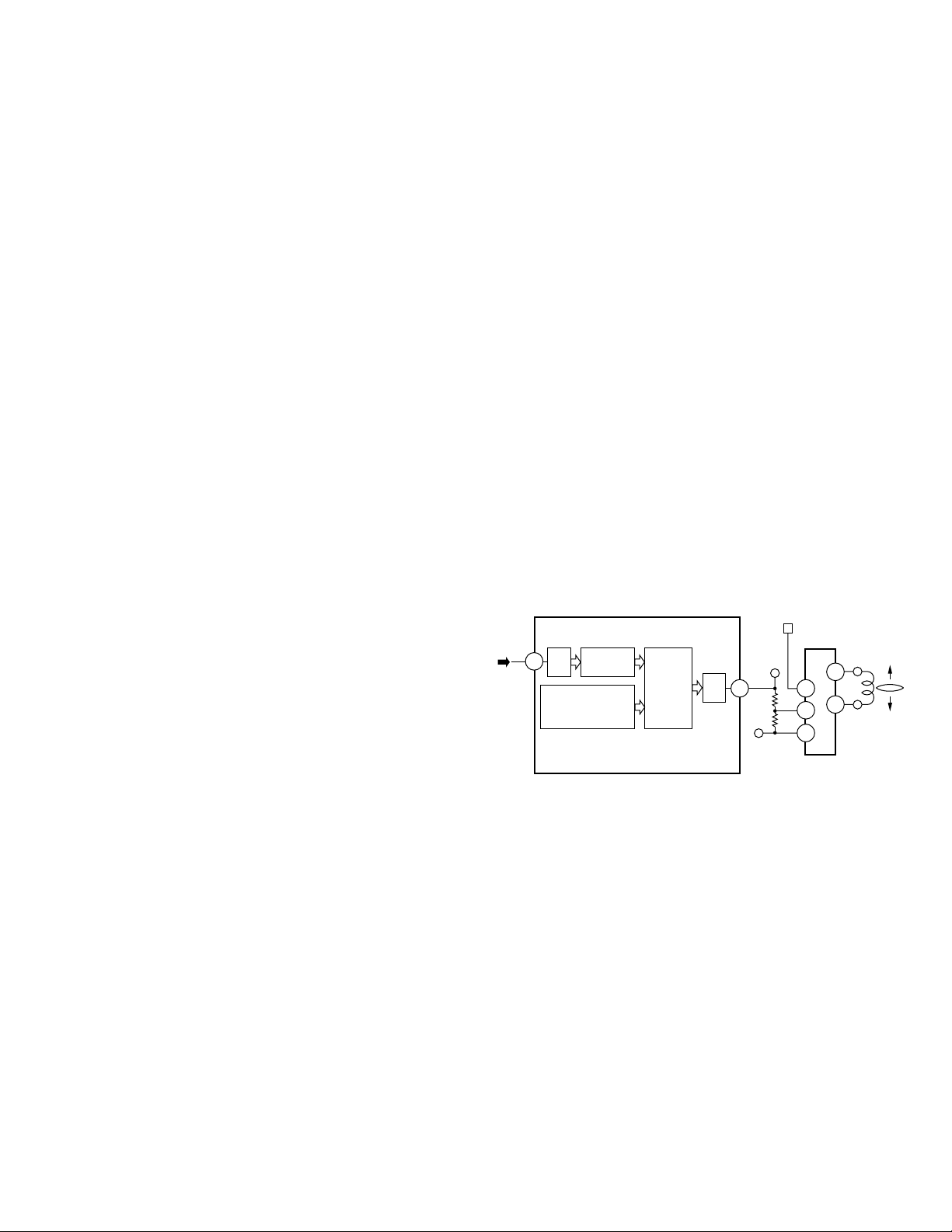
2. CIRCUIT DESCRIPTIONS
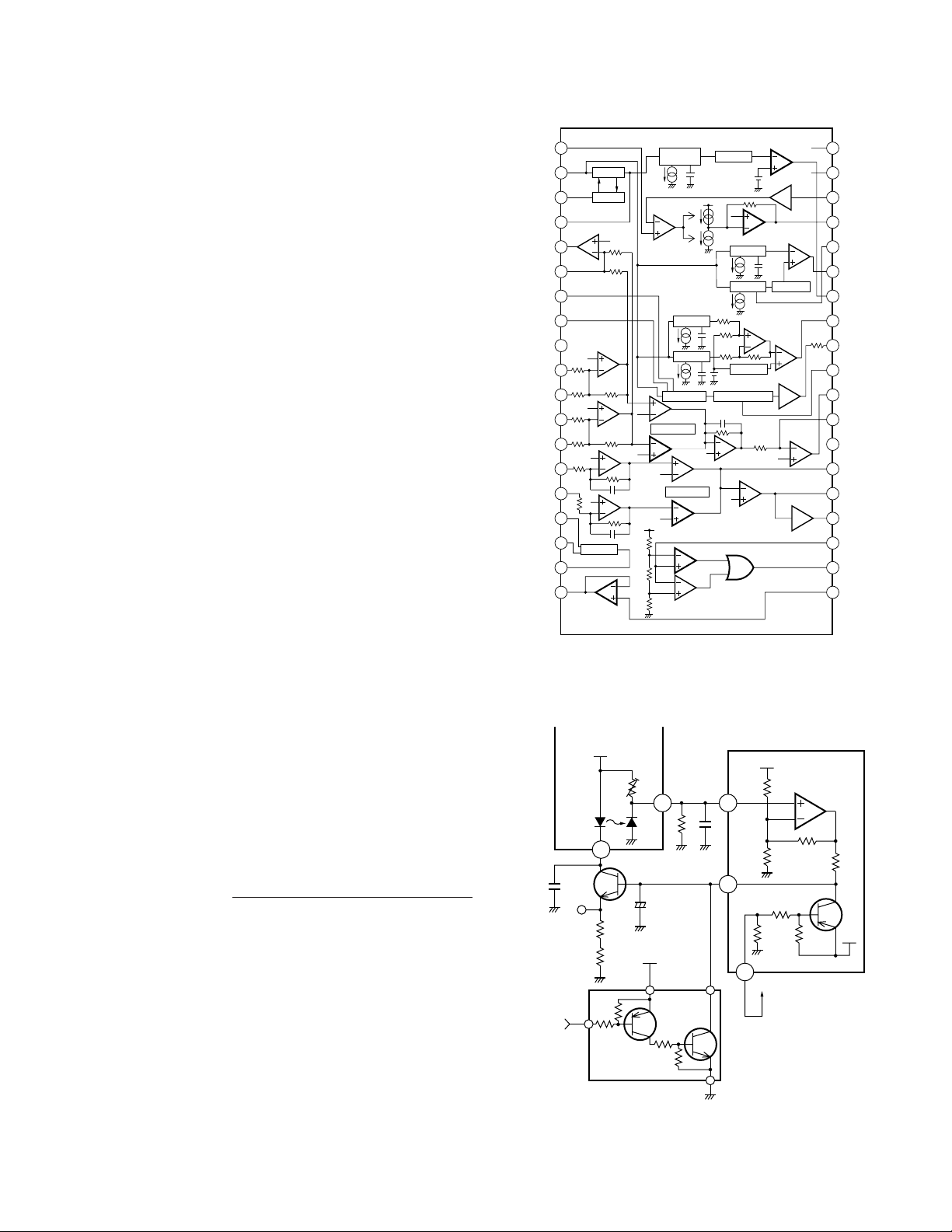
2.1 Preamplifier (UPC2572GS: IC101)
The preamplifier processes pickup output signals to
generate signals to be sent to the servo, demodulator,
and controller. The preamplifier with built-in photodetector converts signals from the pickup into intermediate voltage in the pickup. Then, addition is made in the
RF amplifier (IC101) to obtain RF, FE, TE, and TE zero
cross signals. The system consists of the UPC2572GS
and other components explained below. The system
uses a single power source (+5 V). Therefore, the reference voltage of IC101 and the reference voltage of the
power unit and servo circuit are REFOUT (+2.5 V). REFO
UT is obtained from REFOUT of servo LSI (IC201:
UPD63702GF) via a buffer, and is output from Pin 19 of
IC101. This REFOUT is used as reference for all measurements.
Note:Do NOT short-circuit REFOUT and GND during
measurement.
1
2
3
4
5
6
7
8
9
10
11
12
13
14
15
16
17
18
19
38
37
36
35
34
33
32
31
30
29
28
27
26
25
24
23
22
21
20
X12
RF
envelope
AGC
Detection
X3
Phase detection
3T detection
Bottom
DC shift
Peak
Control
DC shift
Bottom
Peak
120kΩ
DEFECT circuit
FE
BAL
FE
BAL
Vcc
Mirror circuit
FE
BAL
APC
X2
Vcc
FE-BAL
TE-BAL
ASY
EFM-OUT
C.DEF
DEFECT
RFOK
MIRR
3T-OUT
C.FE
FE-OUT
FE-
GND
TE-
TE-OUT1
TE-OUT2
DET-IN
DET-OUT
VREF-INVREF-OUT
LDON
LD
PD
E
F
D
B
C
A
Vcc
C2.3T
C1.3T
RF-
RF-OUT
RF-IN
C AGC
AGC-OUT
EFM-IN
HPF
TE
BAL
EFM comparator
Control
Fig. 1 Block Diagram of UPC2572GS
1) Automatic Power Control (APC) circuit
Laser diode has negative temperature characteristics
with great optical output when the diode is driven with
constant current. Therefore, current must be controlled
by a monitor diode to ensure constant output. Thus
functions the APC circuit. LD current can be obtained by
measuring the voltage between LD1 and GND. The current value is approximately 35 mA.
Vcc (5V)
Vr
LD MD
UPC2572GS
16
PD
17
LD
15
Q101
2SD1664
C124
0.1µF
C101
(100µF/6.3V)
R101
10Ω
LD1
R102
12Ω
5V
CONT
Q102 UMD2N
18
5V
5V
1kΩ
150kΩ
16kΩ
R112
2.2kΩ
C104
0.33µF
5
1kΩ
2.5V
Pickup unit
Fig. 2 APC Circuit
Voltage between LD1 and GND(mv)
LD current(mA) =
10 Ω + 12 Ω
Page 4
4
CX-890
2) RF amplifier and RF AGC amplifier
Photodetector outputs (A+C) and (B+D) are added,
amplified and equalized in IC101, and output to the RFI
terminal as RF signal. (Eye pattern can be checked at
this terminal.)
Low-frequency components of voltage RFI is:
RFI = ((A + C) + (B + D)) x 3.22
where R111 is offset resistor to keep RFI signal within
the output range of the preamplifier. RFI signal is goes
under AC coupling, and is input to Pin 4 (RFIN terminal).
IC101 contains an RF AGC circuit. RFO output from Pin
2 is maintained to a constant level (1.2 ±0.2 Vp-p). The
RFO signal is used in the EFM, DFCT, and MIRR circuits.
3) EFM circuit
The EFM circuit converts RF signal into digital signals of
"0" and "1". RFO signal after AC coupling is input to Pin
1, and supplied to the EFM circuit.
Asymmetry caused during manufacturing of discs cannot be eliminated solely by AC coupling. Therefore, the
system controls the reference voltage ASY of the EFM
comparator by using the fact that probability to generate "0" and "1" is 50% in EFM signal. This reference voltage ASY is generated by output from the EFM comparator through L.P.F. EFM signal is output from Pin 35.
As signal level, amplification is 2.5 Vp-p around
REFOUT.
4) DFCT (defect) circuit
DFCT signal detects mirror defect in discs, and is output
from Pin 33. The system outputs "H" when a mirror
defect is detected.
If disc is soiled, the system determines it as lack of mirror. Therefore, the system inputs the DFCT signal output to the HOLD terminal of servo LSI. Focus and tracking servo drives change to Hold status only when DFCT
output is in "H" so that performance of the system upon
detection of defect can be improved.
5) RFOK circuit
The RFOK circuit outputs signal to show the timing of
focus closing servo, as well as the status of focus closing during playback. The signal is output from Pin 32.
The system inputs the RFOK signal output to the RFOK
terminal of servo LSI. The servo LSI issues Focus Close
command. The system outputs signal in "H" during
focus closing and playback.
CN101
13
6
DETECT
13
11
10
10kΩ
20kΩ
9.3kΩ
RFI
+5V
R111
27kΩ
Vcc
×12
ASY
12
20kΩ
(RF AGC)
AGC
RF
ENVELOPE
HPF
VDC
RFOK
20kΩ
33
36
35
34
PEAK
DEFECT
EFM
UPC2572GS
A+C
10kΩ
B+D
9.3kΩ
20kΩ
10kΩ
10kΩ
R105
6.8kΩ
C125 5pF
C105
24pF
R125
0R0
R104
8.2kΩ
RFIN
C107
4.7µF/35V
C122
0.1µF
C106
RFO
REFOUT (+2.5V)
DEFECT
BOTTOM
R107 8.2kΩ
R106 18kΩ
C111 3300pF
C110
C112 0.047µF
6 54 3 21
32
0.1µF
2200pF
HOLD
Fig. 3 RF AMP, RF AGC, EFM, DFCT, RFOK Circuit
Page 5
5
CX-890
6) Focus-error amplifier
The system outputs photodetector output (A+C) and
(B+D) as FE signal (A+C)-(B+D) from Pin 28 via the difference amplifier, then via the error amplifier.
Low-frequency components of voltage FEY is:
An S curve equivalent to approximately 1.6 Vp-p is
obtained at FE output (Pin 28) by using REFO as reference. The cut-off frequency of the amplifier of the last
layer is 12.4 kHz.
7) Tracking-error amplifier
Outputs E and F from the photodetector are output as
TE signal (E-F) from Pin 24 via the difference amplifier,
then via the error amplifier.
Low-frequency components of voltage TEY is:
TE waveforms equivalent to approximately 1.5 Vp-p are
obtained at TE output (Pin 24) by using REFO as reference. The cut-off frequency of the amplifier of the last
layer is 19.5 kHz.
8) Tracking zero-cross amplifier
Tracking zero-cross signal (TEC signal) is generated by
amplifying TE waveforms (voltage at Pin 24) by a factor
of four. The signal is used for detecting the zero-cross
point of tracking error in the servo LSI UPD63702AGF.
The purposes of detecting the zero-cross point are as
follows:
(1)To be used for counting tracks for carriage move and
track jump.
(2)To be used for detecting the direction of lens move-
ment when tracking is closed. (To be used in the
tracking brake circuit mentioned later.)
The frequency range of TEC signal is from 500 Hz to
19.5 kHz.
Voltage TEC = TE level x 4
In other words, the TEC signal level is calculated as 6
Vp-p. This level exceeds the D range of the operation
amplifier, resulting in the signal to clip. However,
there shall be no problem, since the servo LSI uses
only zero-cross point.
65
9.3kΩ
9.3kΩ
20kΩ
10kΩ
10kΩ
6
13
13
12
10kΩ
10kΩ
20kΩ
FE VCA
38
REFOUT
C114
390pF
FE
R108
33kΩ
28
27
17.2kΩ
50pF
gm=1/68.8kΩ
90kΩ
10
11
CN101
A+C
B+D
F.BAL
REFOUT (+2.5V)
gm CONDUCTANCE
UPC2572GS
Fig. 4 Focus-error amplifier
Fig. 5 Tracking-error amplifier,
Tracking zero-cross amplifier
CN101
R117
16kΩ
R116
16kΩ
14
15
9
11
31kΩ
31kΩ
50pF
63kΩ
C123
4.7nF
R114
10kΩ
R113
10kΩ
TBAL
C115
120pF
R109
68kΩ
R115
1kΩ
C126
15nF
TE
4R
R
F
E
23
TEC
C116
6.8nF
TE VCA
gm=1/17kΩ
63kΩ
37
24
5pF
TOFST
R110
130kΩ
50pF
25
REFOUT (+2.5V)
gm CONDUCTANCE
UPC2572GS
63kΩ 68kΩ
TEY=(E-F) X X
(31kΩ+16kΩ) 17kΩ
: (TE level of pickup unit x 5.36)
20kΩ 90kΩ R108
FEY=(A+C)-(B+D)X X X
10kΩ 68.8kΩ 17.2kΩ
: (FE level of pickup unit x 5.02)
Page 6
6
CX-890
9) MIRR (mirror) circuit
MIRR signal shows ON and OFF track information. The
signal is output from Pin 31.
The status of MIRR signal is as follows:
Laser beam ON track: MIRR = "L"
Laser beam OFF track: MIRR = "H"
The signal is used in the brake circuit mentioned later.
10) 3T OUT circuit
The system detects flickering of RF signal when disturbance is input to the focus servo loop, and outputs the
difference of phase between FE signal and RF-level
fluctuation signal from Pin 30. The resulting signal is
obtained through L.P.F. with a fc of 40 Hz. This signal is
used for automatic adjustment of FE bias.
MIRR
COMP
DC
shift
PeakAGC
Bottom
RFO
Detection
A
1.5V
UPC2572GS
(Peak) – (Bottom)
4
31
RFIN
B
Z
C
RFO
PEAK HOLD
BOTTOM HOLD
MIRROR
1
A
0
False MIRR caused by dirt
True MIRR
OFF TRACK
Dirt, etc.
B
C
Z
Ø
3T-OUT
FE signal
RFIN
UPC2572GS
C113
10nF
FEY
3T detection
C117
0.033µF
120kΩ
L.P.F
Phase detection
8
+
H.P.F
10kΩ
10kΩ
1kΩ
C2.3T
C109
100pF
C1.3T
C108
0.027µF
8
7
30
29
4
AGC
Differential
rectification
3T LEVEL ENVELOPE
DETECTOR
Phase
comparison
Fig.6 MIRR Circuit
Fig. 7 MIRR Circuit
Fig. 8 3T OUT Circuit
Page 7
7
CX-890
2.2 Servo (UPD63702AGF: IC201)
The servo consists of mainly two parts. The first part is
the servo processing unit to equalize error signals and
control track jump, carriage move, in focus, etc. The
second part is the signal processing unit to perform
data decoding, error correction, and interpolation.
The system converts FE and TE signals from analog to
digital in IC201, then outputs drive signals of the focus,
tracking, and carriage systems via the servo block. The
EFM signal input from the preamplifier is decoded by
the signal processing unit, and eventually output as
audio signal after conversion into analog from digital
signals via the DA converter (IC201 contains audio
DAC). Then, the system generates error signal for the
spindle servo in the decoding process, sends the signal
to the spindle servo to generate drive signal for spindle.
After that, drive signals for focus, tracking, carriage,
and spindle are amplified in IC301 and BA5986FM, and
supplied to respective actuators and motors.
1) Focus servo system
The main equalizer of focus servo is located in the
UPD63702AGF. Fig. 9 shows block diagram of the focus
servo.
For the focus servo system, the lens must be positioned within the focusing range in order to perform
focus closing. To achieve this, the system moves the
lens upward/downward by focus-search voltage of triangular waveform to detect the focusing point. During
searching, the system kicks the SPDL motor to maintain rotation speed to set speed.
The servo LSI monitors FE and RFOK signals so that
focus closing is performed automatically at an appropriate point.
Focus closing is performed when the following four
conditions are satisfied:
(1)When the lens moves nearer to the disc.
(2)RFOK = "H"
(3)FZD signal (in IC) is latched to "H"
(4)FE = 0 (REFOUT as reference)
FOCUS
ERROR
D/A
FD
FIN
DRIVER
FOP
FOM
IC301
BA5986FM
LENS
IC 201 UPD63702AGF
76
64
2
4
3
14
13
FOCUS SEARCH
TRIANGULAR WAVE
GENERATOR
DAC
DIGITAL
EQUALIZER
CONTROL
A/D
R301
10kΩ
R302
15kΩ
Fig. 9 Focus servo block diagram
Page 8
8
CX-890
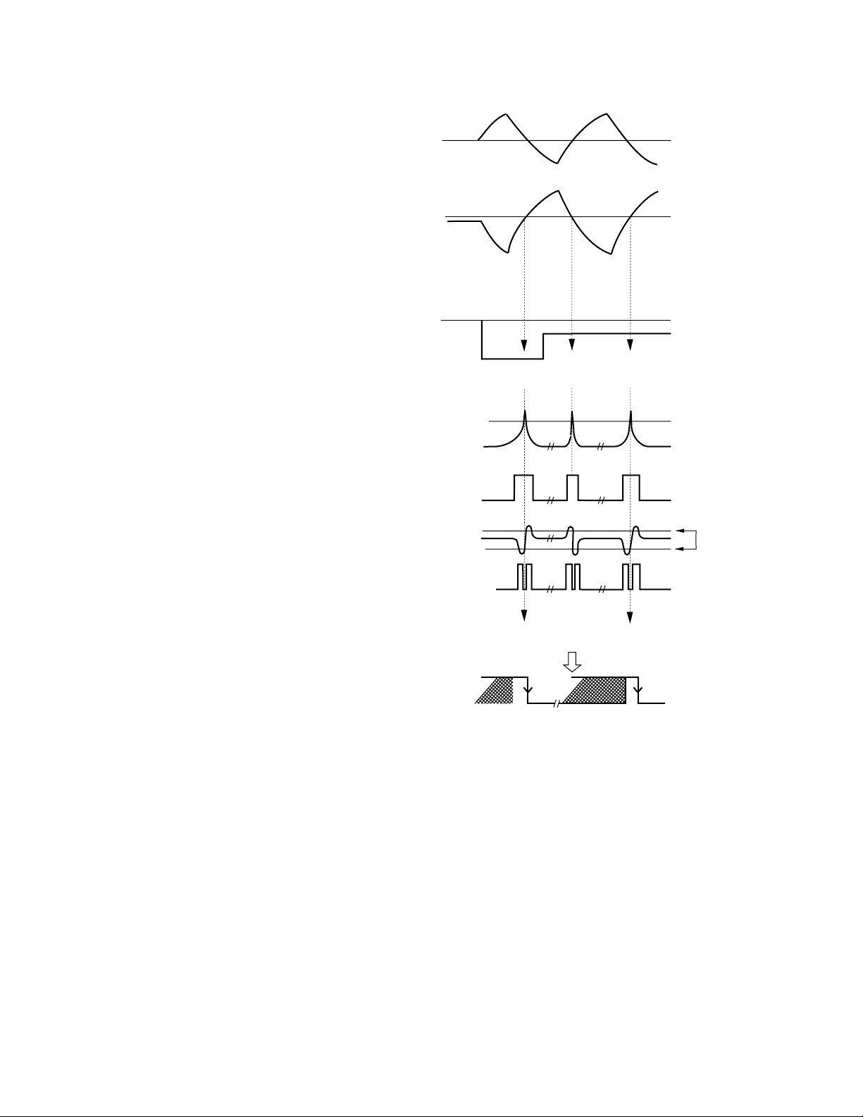
When the conditions mentioned above are satisfied and
focus is closed, the XSO terminal changes from "H" to
"L". Then, the microcomputer starts monitoring RFOK
signal through L.P.F after 40 ms.
If the system judges RFOK signal as "L", the microcomputer takes actions, including protection.
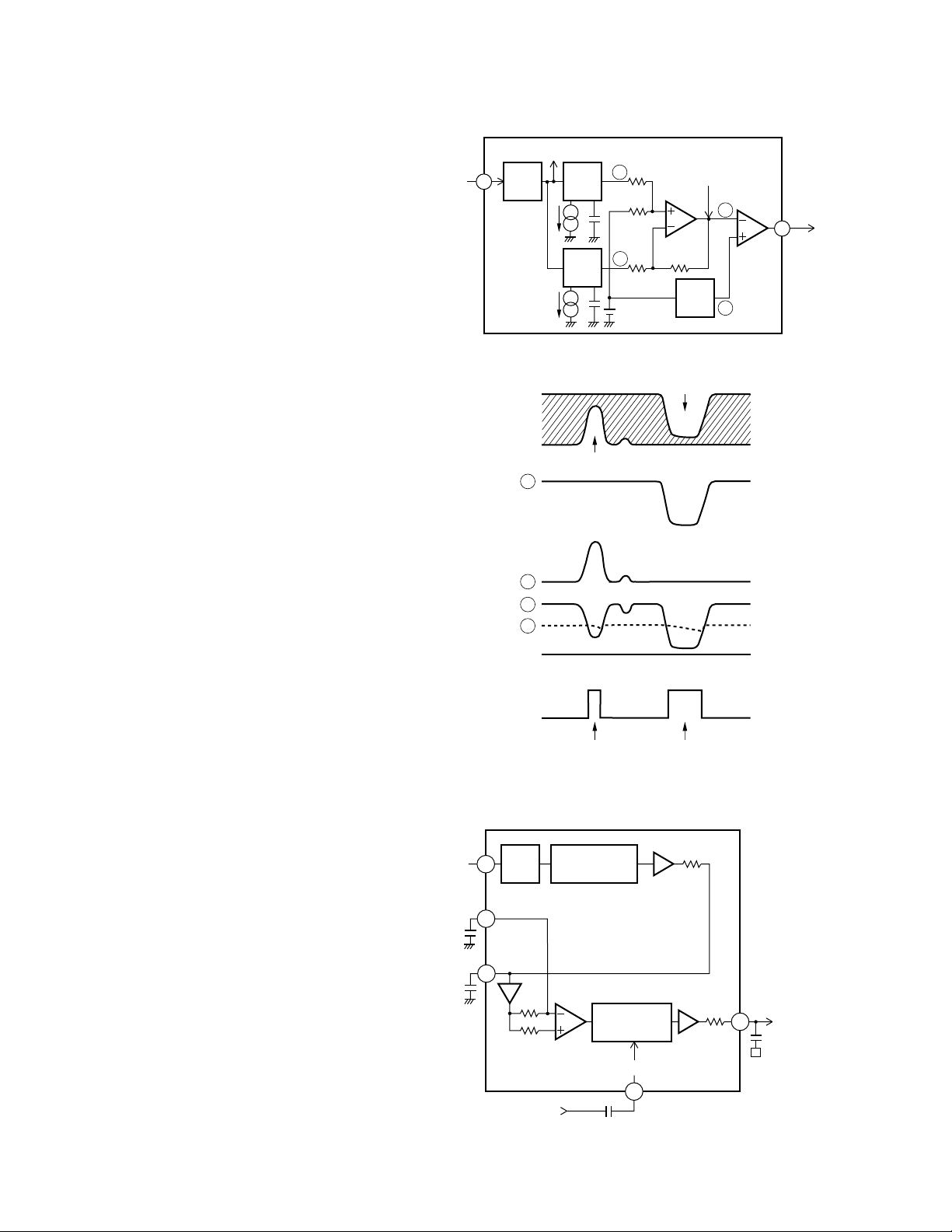
Fig. 10 shows operations related to focus closing. (The
illustration shows when the system cannot perform
focus closing.) S curve, search voltage, and actual lens
behavior can be checked by pressing the Focus Close
button when "01" is shown in Focus Mode Select in Test
mode.
REFOUT
FD
LENS POSITION
RELATIVE TO DISC
NEAR
FAR
"JUST FOCUSED"
SIN
REFOUT
Expanding around "Just Focused Point"
REFOUT
RFI
FOK
FEX
FZD
THRESHOLD
LEVEL
FZD
(INTERNAL SIGNAL)
Focus closing would normally take place at these points
XSO
(IN THE EVENT
FOCUS IS
CLOSED)
LEVEL
Fig. 10 Sequence of Focus Closing
Page 9

9
CX-890
2) Tracking servo system
The main equalizer of tracking servo is located in the
UPD63702AGF. Fig. 11 shows block diagram of the
tracking servo.
a) Track jump
Track jump is automatically performed by the auto
sequence function in LSI when the LSI accepts command. The system has six types of jump (1, 4, 10, 32,
32x2, and 32x3) for truck jump during searching. In Test
mode, the system can select and check these jump
types and CRG move by selecting a mode. The microcomputer sets half of the total number of track jumps
(two tracks if the total number of tracks are four), and
counts the set number of tracks by using TEC signal.
The system outputs brake pulse for a specified time (set
by the microcomputer) from the point of time when the
set number is counted, and stops the lens. Thus, tracking is closed, and the system can continue normal playback.
To improve servo withdrawal during track jump, the
system sets the brake circuit to ON for 60 ms after
brake pulse so that gain of the tracking servo can be
increased.
FF/REV in normal mode is made by continuously performing single jump approximately ten times faster
than in normal playback.
TRACKING
ERROR
D/A
TD
TIN
DRIVER
TOP
TOM
IC301
BA5986FM
LENS
IC 201 UPD63702AGF
77
11
12
JUMP
PARAMETERS
DAC
DIGITAL
EQUALIZER
CONTROL
A/D
5
7
6
R303
10kΩ
R304
27kΩ
63
t1
t2
GAIN NORMAL
TIN
KICK
BRAKE
TEC
T. BRAKE
EQUALIZER
T. SERVO
CLOSED
OPEN
NORMAL
GAIN UP
OFF
ON
t1
TIN
TEC
(10 TRACK)
EQUALIZER
T. BRAKE
SERVO
CIN
2.8mS (4.10 TRACK JUMP)
5.8mS (32 TRACK JUMP)
GAIN UP
NORMAL
ON
OFF
OPEN
CLOSED
t2
60mS
t
Fig. 11 Tracking servo block diagram
Fig. 12 Single track jump
Fig. 13 Multi track jump
Page 10

10
CX-890
b) Brake circuit
Servo withdrawal will deteriorate during setting and
track jump. Thus, the system uses the brake circuit to
provide stable withdrawal to servo loop.
The brake circuit detects the direction of lens movement, and outputs only drive signal in the opposite
direction from the lens movement. Thus, the system
delays the speed of the lens movement to stabilize
withdrawal of the tracking servo.
The system judges sliding direction of track from TEC
and MIRR signals, as well as the relationship of their
phase.
TEC
TZC
(TEC "SQUARED UP" )
(INTERNAL SIGNAL )
MIRR
MIRR LATCHED AT
TZC EDGES
=
SWITCHING PULSE
EQUALIZER OUTPUT
(SWITCHED)
DRIVE DIRECTION
Note: In the illustration, the phase of equalizer output is shown as the same as with that of TEC.
FORWARD
LENS MOVING FORWARDS
(INNER TRACK TO OUTER)
LENS MOVING BACKWARDS
Time
REVERSE
Fig. 14 Tracking Brake Circuit
Page 11

11
CX-890
3) Carriage servo system
Output from low-frequency components (lens position
information) of the tracking equalizer is input to the carriage equalizer by the carriage servo. After obtaining a
certain gain, the system outputs drive signal from the
servo LSI. The signal is then applied to the carriage
motor via the driver IC. More specifically, the pickup
unit as a whole must be moved forward when lens offset during playback reaches a specified level. Therefore,
gain of equalizer is set so that voltage higher than the
activation voltage of the carriage motor is output. As
actual operation, a certain threshold level is set for
equalizer output in the servo LSI, and drive voltage is
output from the servo LSI only when the equalizer output level exceeds that level. Thus, power consumption
is reduced. Depending on eccentricity, etc. of disc, the
equalizer output voltage may cross the threshold level
several times before the pickup unit as a whole starts
operation. At this time, waveforms of drive voltage
from LSI are output as pulse.
D/A
SD
DRIVER
COP
COM
IC301
BA5986FM
CARRIAGE
MOTOR
IC201 UPD63702AGF
62
27
26
25
16
15
KICK, BRAKE
REGISTERS
DAC
DIGITAL
EQUALIZER
CONTROL
FROM
TRACK
EQUALIZER
M
R305
10kΩ
R306
7.5kΩ
CIN
DRIVE ON/OFF THRESHOLD
CARRIAGE MOVED AT THESE POINTS
TRACKING DRIVE
(LOW FREQUENCY)
LENS POSITION
CRG DRIVE
(INSIDE UPD63702AGF)
CRG MOTOR VOLTAGE
Fig. 15 Carriage Servo Circuit
Fig. 16 Carriage Signal Waveforms
Page 12

12
CX-890
4) Spindle servo system
The spindle servo has the following modes:
(1)Kick mode:To be used for accelerating disc rotation
during setting.
(2)Offset mode:
a)To be used after completion of kick until comple
tion of spindle lock during setting.
b)If focus is out of range during playback, this mode
is used until focus is recovered. In both cases,
Offset mode is used for maintaining disc rotation
to the speed close to specified rotation.
(3)Adaptive Servo mode: CLV servo mode during nor-
mal operation. The system samples every WFCK in
16 cycles whether frame synchronous signal matches output from the internal frame counter in EFM
demodulation block, and generates signal that
shows matching/unmatching status. If signal showing unmatching status continues for 8 times, the system deems it as asynchronous status. Except this
case, the system judges as synchronous. In Adaptive
Servo mode, the system automatically selects withdrawal servo for asynchronous status, and steadystate servo for synchronous status.
(4)Brake mode: Mode to stop the spindle motor.
The microcomputer outputs brake voltage from the
servo LSI. Waveforms of EFM are monitored inside
the LSI. If the longest pattern of EFM exceeds specified intervals (if the rotation speed adequately
slowed down), flag is activated in the LSI, and the
microcomputer turns brake voltage to OFF. If no flag
is activated after a specified time, the microcomputer changes from Brake to Stop mode. This status
continues for a specified time. If the system changes
to Stop mode during ejection, disc is ejected after
the specified time mentioned above.
(5)Stop mode: To be used when the power is turned to
ON, and during ejection. In Stop mode, the end-toend voltage of the spindle motor is 0 V.
(6)Rough Servo mode: To be used when returning car-
riage (carriage move during long search, etc.). The
system calculates linear speed from waveforms of
EFM, and inputs either "H" or "L" level to the spindle
equalizer. This mode is also used for confirmation of
grating in Test mode.
MDXMDY
DRIVER
IC301
BA5986FM
IC 201 UPD63702AGF
61
24
22
23
DSP
BLOCK
DAC
DIGITAL
EQUALIZER
EFM
69
SPEED AND
PHASE ERROR SIGNAL
SIN
R308
10k
Ω
R307
10k
Ω
R206
100Ω
Fig. 17 Spindle servo block diagram
Page 13

13
CX-890
2.3 Automatic Adjustment Function
With this system, all circuit adjustments are automatically performed by using the preamplifier (UPC2572GS)
and servo LSI (UPD63702AGF). All adjustments are
automatically performed whenever disc is inserted or
CD mode is selected by the Source key. Details of automatic adjustments are as follows:
1) Setting of FZD cancellation
This setting ensures focus closing. The system reads
the FE offset level when the power is turned to ON,
then writes the inverse voltage of offset value of that
level to CRAM inside IC to cancel offset. Thus, the
threshold level of FZD can be set to a constant value
(+150 mV). As a result, "Latching FZD signal to H",
which is one of the conditions required for focus closing in IC, is ensured.
2) TE offset automatic adjustment
Adjusts TE amplifier offset of the preamplifier to 0 V
when the power is turned to ON.
Adjustment is made as follows:
(1)The microcomputer reads TE offset in LD OFF status
via the servo LSI (TE1).
(2)The microcomputer calculates the voltage to be cor-
rected using the TE1 value, and outputs from Pin 65
(pin name: TOFST) of the servo LSI. More specifically, calculation is made as follows:
TOFST2 = TOFST1 + TE1 x R110 / R109
3) Tracking balance (T.BAL) automatic adjustment
To make the sensitivity of Ech of TE output equal to that
of Fch. In fact, adjustment is made so that the upper
and lower portions of TE waveforms are symmetric to
REFOUT.
Adjustment is made in the following steps:
(1)After focus close, the system kicks the lens in the
radial direction to ensure TE waveforms to be generated.
(2)The microcomputer reads the peak bottom of TE
waveforms via the servo LSI.
(3)The microcomputer calculates the amount of offset,
then calculates the voltage to be corrected based on
that offset. The system outputs the result from Pin 66
(pin name: TBAL) of the servo LSI.
(4)The voltage output from the servo LSI is input to Pin
37 of the preamplifier (IC101: UPC2572GS). Pin 37 is
a control-voltage terminal of the TEVCA amplifier.
According to voltage input, the system changes gain
of Ech and Fch in the preamplifier, and adjusts the
tracking balance to make the upper and lower portions of TE waveforms symmetric to REFOUT.
4) FE bias automatic adjustment
Maximizes the RFI level by optimizing focus point during playback. Adjustment is made by using 3T level
waveforms of RF waveforms and the phase difference
generated by input of disturbance of focus error. Since
adjustment is made by inputting disturbance to focus
loop, the system uses the same timing as with auto
gain control (mentioned later~) for adjustment.
Adjustment is made in the following steps:
(1)Disturbance is input to focus loop by the command
from the microcomputer (inside the servo LSI).
(2)The system detects flickering of 3T components of
RF signal in the preamplifier.
(3)The system checks the phase difference between 3T
components mentioned above and FE signal caused
by input of disturbance to detect the direction of
focus deviation. The result is output as DC voltage
from Pin 30 (3TOUT) of the preamplifier.
(4)The 3TOUT voltage is input to Pin 75 (A/D port) of the
servo LSI. The microcomputer reads this 3TOUT voltage via the servo LSI.
(5)The microcomputer calculates the amount of correc-
tion required. The results are transferred to offset of
focus loop in the servo LSI.
As with auto gain control, the system repeats the
same adjustment process several times to improve
adjustment precision.
Fig. 18 Outline of Automatic Adjustment
AGC
circuit
FE signal
TE signal
Constant RF level
IC101
UPC2572GS
Corrected
voltage
output
Detection
of deviation
Items of
automatic
ADJ
FZD
TE.O
T.BAL
FE.B
F and T.G
D/A
FZD FE.B Gain
A/D
IC201
UPD63702AGF
Transfer
of amount
of correction
Reading
amount of
deviation
System
microcomputer
Calculation
of amount
of correction
RF signal
TE.O, T.BAL
Page 14

5) Auto gain control (AGC)
AGC adjustment is already used in the CD modules of
the previous generation. This function automatically
adjusts servo loop gain of focus and tracking.
Adjustment is made in the following steps:
(1)Disturbance is input to servo loop.
(2)The system extracts error signals (FE and TE) upon
input of disturbance via the B.P.F. and obtains signals
of G1 and G2.
(3)The microcomputer reads G1 and G2 signals via the
servo LSI.
(4)The microcomputer calculates required amount of
correction to adjust loop gain in the servo LSI.
The system repeats the same adjustment process
several times to improve adjustment precision.
6) Initial adjustment value
For all automatic adjustments, the system uses the previous adjustment value as initial values, except when
the power of the microcomputer has been turned to
OFF (backup is turned to OFF). If backup has been
turned to OFF, the system uses initial set value to perform automatic adjustment.
7) Display of coefficients of adjustment results
Results of automatic adjustments can be displayed in
Test mode for confirmation. Display of coefficients in
each automatic adjustment is as follows:
(1)FZD cancel, TE.OFST cancel, T.BAL, and FE bias
Reference = 32 (32: No adjustment was required)
Display is made in units of approximately 40 mV.
Example: Coefficient of FZD cancel = 35
35 - 32 = 3 3 x 40 mV = 120 mV
Corrected amount is approximately +120 mV.
Thus, FE offset before adjustment is -120 mV.
(2)Adjustment of F and T gain
Reference: Focus = 13, tracking = 20
The amount of reduced gain in comparison with the
reference is known by looking at the coefficient dis
played.
Example: AGC coefficient = 40
Amount of reduced gain = 20 log (20/40) = -6dB
2.4 Power Supply and Mechanism
Control
The power supply VM (7.5V) is produced from the
power supply VD (9.0V) supplied from the extension
P.C. board, and used as the power supply for the loading motor driver, elevation motor driver, cam gear
motor driver, and 5V Reg IC. As for the drive voltage
for the disc detection LEDs and the power supply for
the CD driver ICs, the power supply VD (9.0V) is used.
The system IC controls the ON/OFF operations of the
CD driver and laser diodes,the 5V power supply, and
the drive voltage PVD for detection LEDs with "CONT",
"POWER", and "LOAD" signals respectively.
14
CX-890
Page 15

15
CX-890
2.5 STS(Sure Track System) Circuit
By pooling the musical data read in from a compact disc into the memory, even if the pickup should go off track for
some reason, the Sure Track System enables prevention of sound interruption during recovery (approximately 3 seconds) by continuing to output data from the memory.
Operation Principle
The STS circuit is controlled by the vibration free memory controller (CXD2511R). Data read in at double speed
from a compact disc is input via the digital signal processing circuit into CXD2511R.
CXD2511R stores this DA data in DRAM (MSM5114400
DP-60TS), and reads and outputs the data at normal
speed in synchronization with the internally generated
FS system clock. In order to write the DA data at double
speed and to read out at normal speed, the DRAM
becomes full, but when it reaches capacity it will tentatively stop reading data. (The CD is in the pause mode
during this time.) When an available area is created by
data read-out from the DRAM, data writing will start
again. (The available area of the DRAM can be monitored by ADRMON. By repeating this process, the
DRAM is always used effectively, and approximately
2.67 seconds worth data can be stored. Even if the pickup should go off track due to vibrations for example, if
recovered within 2.67 seconds while using the memorized data, sound interruption can be prevented.
Fig. 19
Fig. 20
Page 16

16
CX-890
3. MECHANISM OPERATIONS
3.1 Disc Insertion
a)The Cam gear rotates to the elevation OK position
(See "How to remove the Tray Assy" on page 21). The
Stage Mech Assy moves upwards or downwards to
reach the height of the selected tray by using the elevation mechanism.
b)The Cam gear rotates counterclockwise until the
LOAD switch is turned off. The Beak arms of the
Stage Mech ASSY driven by the Cam gear's movement lift the selected tray.
c)The Stage Mech Assy with the tray lifted moves to the
top position using the elevation mechanism.
* Disc insertion/ejection is performed at the top position
(the 6th stage) irrespectively of tray position.
d)The Cam gear rotates counterclockwise to move the
LOAD arms as shown in Fig.21.
e)The LOAD arms push the disc loaded on the tray and
open the tray hooks.
f)When a disc is inserted, the disc interrupts the infrared
LED light from the photo transistors, and the Rubber
roller starts rotating.
* The photo transistors are connected in serial. When
the light is interrupted from either photo-transistor,
the start of disc insertion will be detected.
g)The disc is drawn in. Then the disc pushes the inser-
tion completion switch via the arm.
h)The LOAD arms move forward to be released from
the disc. At the same time, the tray hooks close to
hold the disc on the tray.
Cam gear
Load switch
Beak arm
Stage mech Assy
Load arm
Load arm
Insertion completion switch
Disc
Tray hook
Load arm
Photo transistors
Fig. 21: Elevation OK position
Fig. 22
Page 17

17
CX-890
3.3 Elevation Detection
a)The elevation detection (slit count) is performed by
the photo interrupter.
b)After the elevation HOME switch is turned ON, the
photo interrupter counts the slits of the elevation
levers.
* The bottom position (the 1st stage) is detected when
the elevation HOME switch is turned on (not detected
by the photo interrupter).
3.2 Elevation
a)The Cam gear rotates to the elevation OK position.
b)The ELV motor rotates to slide the elevation lever via
the gears.
c)The 2 elevation levers (left and right) can synchronize
their sliding via the joint arm.
d)The shafts of the Stage Mech Assy engage with the
stair-like grooves in the elevation levers and the verti-
cal holes in the Main chassis via the rollers.
e) When the elevation levers slide, the Stage Mech Assy
moves up and down.
ELV motor
Photo interrupter
Elevation lever
Elevation
HOME switch
joint arm
Elevation lever
Fig. 23
Page 18

18
CX-890
3.4 Disc Clamp
a)The Stage Mech Assy moves up and down to reach
the height of the selected tray, using the elevation
mechanism.
b)The Cam gear rotates clockwise, the Carriage drive
arm rotates, and then the Carriage Mech Assy moves
toward the disc via the Carriage drive shaft.
c)The Cam gear continues rotating clockwise and the
Carriage drive shaft moves the Clamp UP lever. Then
the Clamp arm touching the Clamp UP roller moves
down to clamp the disc.
d)The Cam gear stops when the Clamp switch is turned
ON.
Clamp UP lever
Clamp arm
Clamp UP roller
Carriage Mech Assy
Carriage drive shaft
Carriage drive arm
Clamp switch
Fig. 24
3.5 Disc Sense (Initializing)
a)The disc sense operation is to detect if or not a disc is
loaded on the trays 1 to 6.
b)While a disc is inserted using the robber rollers, the
disc pushes the insertion completion switch via the
arm to sense that a disc is loaded.
3.6 Disc Ejection
a)The same operations as the steps a) to e) on "3.1 Disc
insertion" are performed.
b)The rubber roller(s) rotate(s) in the direction for disc
ejection.
c)When the infrared LED light, which has been inter-
rupted by the disc, passes toward the photo transistors, the rubber rollers stops.
Page 19

19
CX-890
3.7 Mechanism Lock
a)Mechanism lock operation is to push the mechanism
downward and toward the disc slot in order to keep
the mechanism at the correct position during disc
insertion/ejection, and to leave the appropriate gap
above the mechanism.
b)The Cam gear rotates to move the Mech lock lever
toward the rear of the Mechanism. The lever pushes
the inside surface of the product. It causes the mechanism to move forward.
c)With the movement of the Mech lock lever, the Mech
lock lever (right) moves in a slanting direction as indicated by the arrow in Fig. 25 to push the mechanism
forward and downward.
d)The Mech lock lever (left) is driven by the movement
of the Mech lock lever via the Mech lock junction
lever to push the Mechanism downward.
e)The mechanism lock is released only in the disc
clamp mode.
Mech lock lever
Mech lock lever (left)
Mech lock junction
lever
Mech lock lever (right)
Fig. 25
Door switch
Door lever
Cam gear
Door open lever
Fig. 26
3.8 Door Open
a)The Door open lever pushes the door on the product
grille to open it.
b)The Cam gear rotates to move the door arm. Then,
the door arm moves the door lever.
c)The door lever moves the door open lever via the
buffer spring.
d)When the door switch is turned ON, the Cam gear
motor stops rotating.
Page 20

20
CX-890
3.9 Stage Mechanism Lock
a)To prevent the Stage mech assy from rattling during
disc play, which may adversely affect the vibrationresistant performance, the Stage lock function works
only in the disc clamp mode.
b)In the mode described at the step c) on "3.7
Mechanism lock" , the Stage lock lever (right) is driven by the movement of the Mech lock lever (right).
c)The 2 bent portions of the Stage lock lever (right) are
pressed against the gear-like portions of the chassis
to lock the right side of the Stage mech assy.
d)For the left side of the Stage mech assy, in the mode
described at the step d) on "3.7 Mechanism lock", the
Mech lock junction lever is driven to move the Stage
lock lever (left).
e)The 2 bent portions of the Stage lock lever (left) are
pressed against the gear-like portions of the chassis
to lock the left side of the Stage mech assy.
Mech lock lever (right)
Stage lock lever
(right)
Stage lock lever
(right)
Chassis gear-like portion
(View from the opposite side)
Fig. 27
Page 21

21
CX-890
4. DISASSEMBLY
- How to remove the Tray Assy
1. Apply about 6V current to the Cam gear motor until
all holes match at the position (A) (elevation OK position).
2. Hook the three springs B temporarily as shown in Fig.
28. While pushing the Tray holder lock arms (right
and left) in the direction (C), remove the Tray holder.
3. Lift up the Tray assy to remove it.
* Be careful not to remove the Tray hooks from the Tray
assy.
- How to remove the Carriage Mech Assy
1. Insert a short pin into the flexible PCB of the Pickup
unit.
2. While opening the resin hooks, remove the cover
from the Servo unit.
3. Disconnect the flexible PCBs from the connectors
CN101 and CN301.
4. Remove the Tray holder and the Tray assy. (See
above)
5. Rotate the Cam gear motor until the positions of all
holes (E) match, then stop the motor.
(The Carriage Mech assy will stop as shown in the
Fig.30.)
* When the positions of all holes match, they will be
completely covered by the Carriage mech assy.
* To rotate the Cam Gear motor, see "How to remove
the Tray assy".
6. Unhook the spring A.
7. Remove the flexible holder B (while opening the
hooks).
8. Remove the flexible PCB (C) from the motor. (The
flexible PCB (C) has been stuck on the motor with
double-sided adhesive tape.)
9. Loosen the fixing screw and remove the flexible
holder.
ELV motor
Cam gear motor
Approximately DC 6V
Tray holder
Tray holder lock arm
Tray holder
lock arm
Tray
hooks
Tray Assy
Cover
CN101
CN301
Match the hole positions
Flexible
holder
Fig.28
Fig. 29
Fig. 30
Short pin
Tray
hooks
Page 22

22
CX-890
- How to remove the Pickup unit
1. Remove the pulling spring, torsion spring and Eshaped ring. Then remove the Clamper arm.
* The spring (A) will be removed with the Clamper
arm.
10. Remove the screw, pressure spring and collar. Lift
up the Carriage mech assy to remove it.
* Screw tightening torque: 2.6kgfcm
2. Slide the Clamp UP lever (B) to remove it.
3. Loosen the 2 screws. Remove the feed-screw cover
by sliding it.
4. Remove the feed-screw pressure spring (D).
5. Loosen the 2 screws. Remove the feed-screw holder
(E).
6. Remove the belt.
7. Remove the Pickup unit together with the feed screw.
* Be careful not to lose the shaft holders at the both
ends of the feed screw.
* Be careful not to damage the 2 flexible PCBs(for the
Pickup and motor) when separating them. The flexible PCBs have been stuck each other with doublesided adhesive tape.
Carriage mech
Assy
Screw
Collar
Pressure spring
Clamper arm
E-shaped ring
Pulling spring
Torsion spring
White
Black
Pickup
unit
Feed screw
Belt
Carriage
motor
Fig. 31
Fig. 32
Fig. 33
Page 23

23
CX-890
8. Loosen the 2 screws. Remove the plate spring and
the rack.
9. Pull out the feed screw from the Pickup unit.
- How to remove the Carriage Motor Assy
1. Loosen the 2 screws (A). Remove the Carriage
motor assy.
- How to remove the Spindle Motor Assy
1. Remove the connector.
2. Loosen the 2 screws (B). Remove the Spindle motor
assy.
- How to remove the Cam gear motor and ELV
motor
1. Insert a short pin into the Pickup flexible PCB.
(See Fig. 30)
Remove the Cover from the Servo unit. (See Fig. 30)
Disconnect the flexible PCBs from the connectors
CN101 and CN301. (See Fig. 30)
2. Disconnect the the flexible PCB (Motor PCB(A)) from
the connector CN201 on the Servo unit.
3. Disconnect the flexible PCB from the connector
CN801 on the STS unit.
4. Loosen the 2 screws (A). Remove the Servo unit.
5. Loosen the screw (B). Remove the flexible PCB holder.
6. De-solder at the 4 portions (C). Remove the flexible
PCB.
Rack
Plate spring
Feed screw
Pickup
unit
Spindle motor
assy
Carriage motor
assy
Servo unit
Motor PCB (A)
Flexible holder
C
N
201
Front
Grease (White: KD-1)
Grease (Yellow:
PG-641)
Fig. 34
Fig. 35
Fig. 36
Grease (Yellow:
PG-641)
Page 24

24
CX-890
9. Remove the 5 polyslider washers, then gears and
shaft.
10. Loosen the 4 screws. Remove the Cam gear motor
and ELV motor.
7. Loosen the 2 screws (D). Remove the Gear cover.
8. Loosen the 3 screws (E). Remove the Motor bracket
assy.
- How to remove the Loading motor
1. Insert a short pin into the flexible PCB of the Pickup
unit.(See Fig. 30)
Remove the Cover from the Servo unit. (See Fig. 30)
Disconnect the flexible PCBs from the connectors
CN101 and CN301. (See Fig. 30)
Disconnect the the flexible PCB (Motor PCB (A)) from
the connector CN201 on the Servo unit. (See Fig. 36)
2. Unhook the spring. Remove the Door open lever.
3. Loosen the 3 screws. Remove the PCB units (C) & (D)
and the frame.
4. Remove the spring (A).
Gear cover
Motor bracket
assy
Front
Cam gear motor
ELV
motor
Spring
Door open lever
PCB (C)
Frame
Black
White
PCB (D)
Apply grease (White:EM50L) to the Shaft and
gears.
Fig. 37
Fig. 38
Fig. 39
Shaft
Black
Page 25

25
CX-890
5. Remove the belt (large).
6. De-solder at the points (B) and (C).
7. Loosen the 2 screws. Remove the Loading motor
bracket.
8. Remove the belt (small).
9. Loosen the 2 screws. Remove the Loading motor.
- How to remove the Stage Mech Assy
1. Remove the Tray holder and the Tray assy. (See Fig.
28)
Remove the Carriage mech assy. (See Fig. 30 and
31)
Remove the Servo unit. (See Fig. 36)
Remove the Motor PCB (A). (See Fig. 36)
Remove the Gear cover. (Fig. 37)
2. Unhook the Spring (C). Remove the Door-open lever.
3. Loosen the screws (D), (E), and (F). Remove the PCB
(C) and (D), and the frame.
4. Unhook the springs (A) and (B).
5. Pull out the Load arm assy (right) upward.
6. Unhook the spring (G). Remove the belt (large).
7. Loosen the screw (H). Remove the Load arm assy
PCB (E)
Loading motor
Loading motor bracket
Belt
(small)
Belt (large)
PCB (D)
Door open lever
Load arm
assy (left)
Load arm assy (right)
PCB (C)
Frame
Fig. 40
Fig. 41
Page 26

CX-890
(left) including the Loading motor.
8. Loosen the 4 screws. Remove the Motor bracket
assy and Photo interrupter.
9. Remove the 4 E-shaped rings (A) and 3 wash-
ers (B).
10. Remove the Mech lock lever (left).
11. Remove the 2 rollers (C).
12. Remove the Elevation lever (left). (Pay
attention to the mounting direction.)
13. Remove the Mech lock junction lever and
and roller (D).
(Pay attention to the mounting direction.)
14. Remove the 2 E-shaped rings (A) and 2 washers (B).
15. Remove the Elevation lever (right).
16. Remove the 2 rollers (C). (Pay attention to the
mounting direction.)
17. Remove the Mech lock lever (right).
18. Lift up the Stage mech assy to remove it.
Motor bracket assy
Photo interrupter
Front
Mech lock junction lever
Elevation lever (left)
Mech lock lever (left)
Mech lock lever (right)
Elevation lever (right)
Stage mech assy
Fig. 42
Fig. 43
Fig. 44
 Loading...