PIONEER CX 683 Service Manual

PIONEER CORPORATION 4-1, Meguro 1-Chome, Meguro-ku, Tokyo 153-8654, Japan
PIONEER ELECTRONICS SERVICE INC. P.O.Box 1760, Long Beach, CA 90801-1760 U.S.A.
PIONEER EUROPE N.V. Haven 1087 Keetberglaan 1, 9120 Melsele, Belgium
PIONEER ELECTRONICS ASIACENTRE PTE.LTD. 253 Alexandra Road, #04-01, Singapore 159936
C PIONEER CORPORATION 2000
K-FZU. JAN. 2000 Printed in Japan
ORDER NO.
CRT2441
MD MECHANISM MODULE
CX-683
NOTE:
- This Service Manual describes the operations of the MD mechanism module being used for the models
listed in the Table indicated below.
- Be sure to reference this service manual as well as the service manual prepared for respective models
must be referenced before implementing the repair work.
CONTENTS
1. CIRCUIT DESCRIPTIONS...........................................2
2. MECHANISM DESCRIPTIONS.................................12
3. DISASSEMBLY .........................................................15
MODEL SERVICE MANUAL MD MECHANISM MODULE
MEH-P5100R/EW CRT2445 CXK3110

1. CIRCUIT DESCRIPTIONS
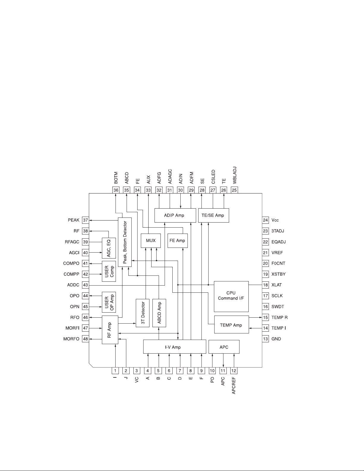
1.1 RF AMPLIFIER BLOCK (CXA2523AR : IC101)
This section works to process the output signals from the MD pickup to generate signals to be transferred to the next
stage, namely, the DSP section (IC201).
Respective photo-detector output signals A, B, C, D, E and F are I-V converted and processed inside the RF amplifier to
become FE, TE and ADIP signals.
Also, I and J outputs which have been I-V converted by the amplifier incorporating the photo-detector inside the
pickup are processed to become the RF signals and the PEAK and BOTM signals.
Meanwhile, since this system is of the single power (+3.3V) specification, the reference voltage for the servo-signals is
Vc (1.65V).
Vc is being output from this RF amplifier (IC101, 3pin).
(Note) Do not short the Vc and GND while making measurements.
2
CX-683
Fig. 1 : CXA2523AR BLOCK DIAGRAM

3
CX-683
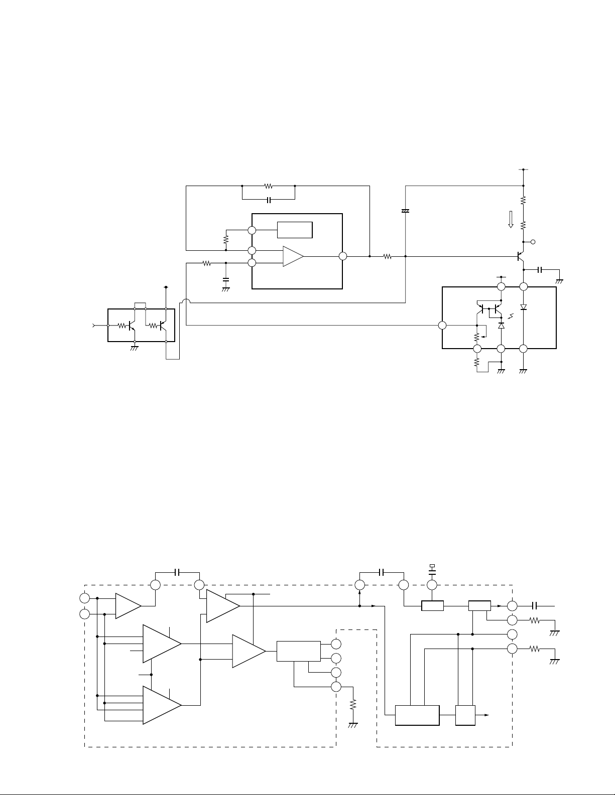
2) RF Amplifier
I and J signals being I-J converted in the pickup are entered to 1 and 2 pins. Then, their difference signal (group
signal) and sum signal (bit signal) are generated on RFA1 and RFA2, respectively.
RFA2 and RFA3 are switching operational amplifiers. The amplifiers detect high reflection (Premastered) and low
reflection (Recordable) using the disc detector switch (S404) to switch to the gain selected by the serial command
HLPT or PTGR.
RF signal (46 pin) is operated and conducted to the AGC circuit and equalizer via C122 to generate RF signal (36 pin).
RF signal is maintained essentially at a constant level (approximately at 1.1 Vpp) by the AGC circuit.
This signal is entered to the signal processing LSI (IC201: 55 pins) for the data processing as well as control of the
Premastered Disc playing spindle.
1) APC (Automatic Power Control) Circuit
Since laser diode (LD) has temperature characteristics, the APC circuit is provided to control current flow using the
monitor diode so that the output may be kept at a constant level.
LD current is determined by measuring voltage across V1 and 3VD.
The current value should be approximately 40 mA (0.4V/10
Ω).
19
20 6
10
12
11
–
+
21
12 14
13
VREF
Q102
UMD2N
LDCNT
R103
PD
APC REF
CXA2523AR
MON
Vr
MD
LD
3VD
C105
R1
LD+
3VD
R102 0R0
R101 10
VI
100/6R3
R108
APC
C108 R001
R109 470K
R110
6R8K
1.25V
6R8K
C106
+
GNDVR
R104
0Ω
LD –
PU unit
47K
C107
3VP
22P
1
2
38
–
+
–2
–1
–1
–2
–1
–2
–1
–1
–1
–2
–2
48 47
22
20
22
46 40 39
25
20
36
37
Peak/Bottom
Hold
BPF
fo=720kHz
Peak
Hold
BPF3T PEAK3T
PBH1
J
MORFO MORFI RFO
I
RFA1
OFST
ABCD
RFA3
PEAK
BOTM
F0CNT
WBLADJ
PBSW
GRVA
HLPT
GRV
RFA2
PTGR
AGC EQA
3TADJ
F0CNT
I3
EQADJ
RFAGC
<To IC201>
RF
C122
R022
C124
R047

4
CX-683
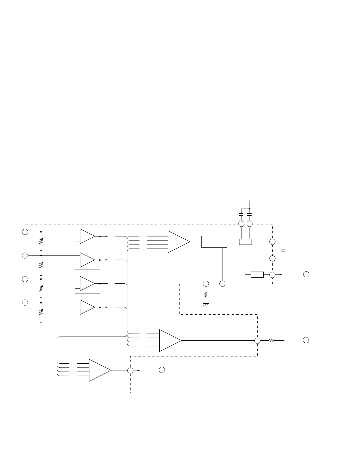
3) I-V, ADIP, ABCD and FE Amplifier Blocks
They are used for I-V conversion of photo-detector signals (A to F pins) from the pickup.
ADIP, FE and full quantity of light signals are generated from A to D signals, and TE signal is generated from E and F
signals.
The ABCD amplifier generates the full quantity of light signal for the main spot. This signal is sum of A to D signals
after I-V conversion. According to the level of the full quantity of light signal, resistance value of I-V is automatically
adjusted so that ADIP, FE and TE signals may be maintained at the specified level.
FE and TE signals output from both the Recordable and Premastered Discs are adjusted to approximately 1 Vpp and
1.7 Vpp, respectively. This adjustment is executed whenever a disc is inserted.
ABCD signal entered to the signal processing LSI (IC201: 64 pins) is also used for generating FOK and defect detect
signals.
The ADIP amplifier is used for generating ADIP signal that is present only on the Recordable Disc.
Addresses are already recorded on the Recordable Disc by wobbling FM signal that uses 22.05 KHz as the carrier. In
order to detect wobble elements, noise elements of the signal are eliminated on the BPF, then the signal is output to
the ADFM via the AGC. The signal is then sent to C111 for DC cut and binary converted on the comparator to generate
ADFG signal. ADFG signal is entered to the signal processing LSI (IC201: 78 pins) to control the address and spindle
when the Recordable Disc is played.
–
–
+
+
4
+
–
5
+
–
6
+
–
7
25
+
–
–
–
+
+
–
–
–
–
35
64
34
29
30
32
65
78
20
43 31
Focus err amplifier
IVR0-IVR4
FE
R219
100
AIV
A
AA BB
CC
AA
DD
AA
CC
BB
DD
AA
BB
CC
DD
IVR0-IVR4
BIV
B
ABCD
BB
IVR0-IVR4
CIV
C
CC
IVR0-IVR4
DIV
ABCDA
FEA
ATA
D
DD
ADAGC
ADFM
ADIN
WBLADI
F0CNT
ADFG
ADDC
C11
4700P
<To IC201 pins>
BPF
fo=22.05kHz
BPF22
ADIPAGC
<To IC201 pins>
<To IC201 pins>
AGC
BPFC
COMP
ABCD amplifier
I-V amplifier ADIP amplifier

5
CX-683
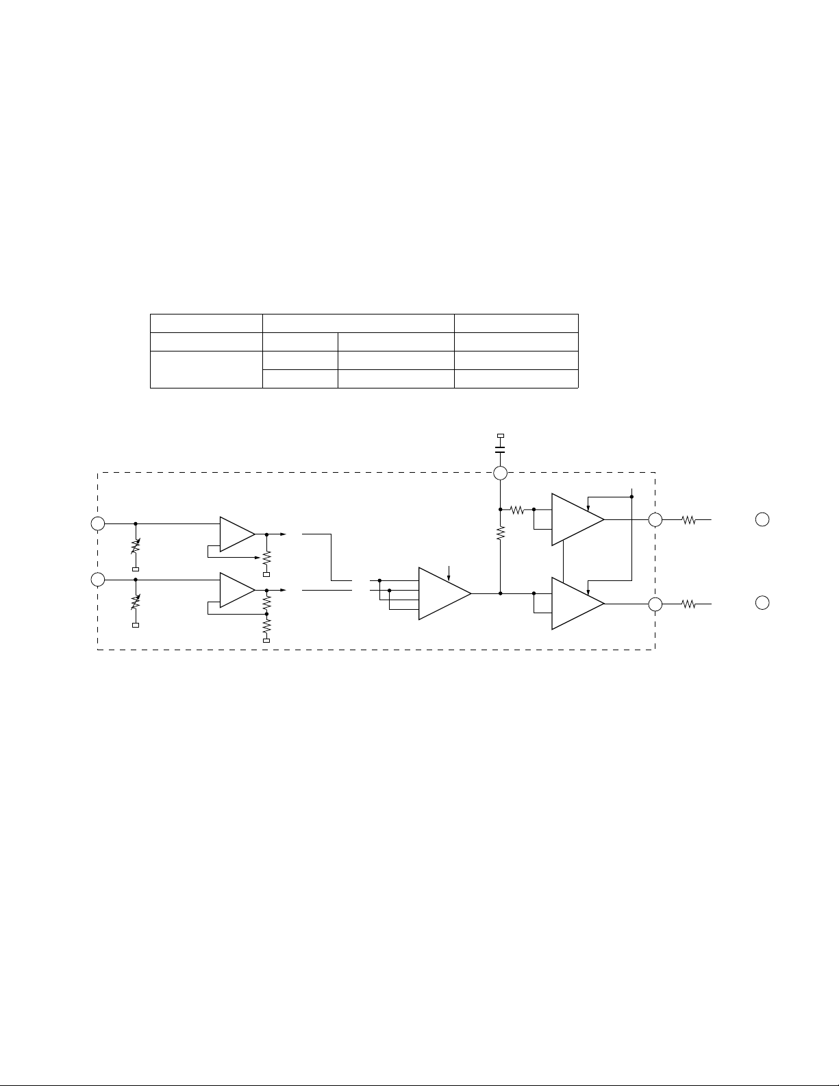
4) TE and SE Amplifiers
Side spot E and F signals are I-V converted, then entered to the EF balance adjusting amplifier. Then, after polarity of
the tracking error signal is switched by the TE differential amplifier (TESW), the signal is conducted to the gain
amplifier to generate TE signal.
Select PTGR = 1 for the Pit play and PTGR = 2 for the group play.
The EF balance adjusting amplifier automatically adjusts an EF balance resistance value so that level of SE signal
becomes the same as the reference voltage Vc when the TRKG made is open.
The SE amplifier generates TE signal from the LPF, then enters it into the signal processing LSI (IC201: 73 pins) for
digital equalizing.
Condition PTGR HLPT
PremasterdDisc Pit High reflection 1 2
RecordableDisc Pit Low reflection 1 1
Groove Low reflection 2 1
–1
+1
+2
–2
8
+
–
9
+
–
26
27
–2
–1
74
28
–2
–1
73
IVR0-IVR4
EFB0-EFB4
EIV
E
EE
EE
FF
IVR0-IVR4
FIV
F
FF
CSLED
TG
TEA
TESW
PTGR
TE
<To IC201 pins>
R221
SEA
SE
<To IC201 pins>
R220
100
100
C110
R068
Pit / GR Select
Pit
GR
 Loading...