

Page 1
PIONEER CORPORATION 4-1, Meguro 1-chome, Meguro-ku, Tokyo 153-8654, Japan
PIONEER ELECTRONICS (USA) INC. P.O. Box 1760, Long Beach, CA 90801-1760, U.S.A.
PIONEER EUROPE NV Haven 1087, Keetberglaan 1, 9120 Melsele, Belgium
PIONEER ELECTRONICS ASIACENTRE PTE. LTD. 253 Alexandra Road, #04-01, Singapore 159936
PIONEER CORPORATION 2006
ORDER NO.
CRT3655
DVD MECHANISM MODULE(MS4)
CX-3183
This service manual describes the operation of the DVD mechanism modules
incorporated in the models listed below.
When performing repairs use this manual together with the specific manual for the
model under repair.
Model No. Service Manual DVD Mechanism Module
AVH-P7800DVD/UC CRT3681 CXK6500
AVH-P7800DVD/RE CRT3682 CXK6500
CONTENTS
1. CIRCUIT DESCRIPTIONS(FE PART) . . . . . . . . . . . . . . . . . . . . . . . 2
2. CIRCUIT DESCRIPTIONS(BE PART) . . . . . . . . . . . . . . . . . . . . . . 11
3. MECHANISM DESCRIPTIONS . . . . . . . . . . . . . . . . . . . . . . . . . . . 17
4. DISASSEMBLY. . . . . . . . . . . . . . . . . . . . . . . . . . . . . . . . . . . . . . . . 21
K-ZZU. MAY 2006 printed in Japan
Page 2
1234
1. CIRCUIT DESCRIPTIONS(FE PART)
A
1 Front End Part (MN2DS09AAUB:IC1501)
MN2DS09AAUB are 1-chip LSI for DVD-Player. The connection of this LSI to the Driver IC,
SDRAM, Flash-ROM, Audio-DAC, etc. can configure the DVD-Player System.
This LSI contains Front End (SODC/FE) that performs RF signal /Servo /Decode processings, Back End
(AV decoder/BE) that performs the video decode processing such as MPEG1/MPEG2/JPEG and audio decode
processing such as DVD-Audio/Dolby Dijital/DTS/MP3, and the system controller (Siscon) for controlling
the system.
Front End part realizes the arithmetic processing of optical head signal and RF signal processing,
the digital signal processing for DVD-ROM reproduction that conforms to DVD standards (16-8 Demodulation,
Error correction), the digital signal processing for CD-DA/CD-ROM (Error correction), AV decoder transmission,
servo control, spindle motor control and seek control.
Please take note that, The waveform of servo system on the front end, FE, TE and AS is not
B
seen in MN2DS09AAUB,like the DVD mecha-module (MS3V1) of CX-3078.
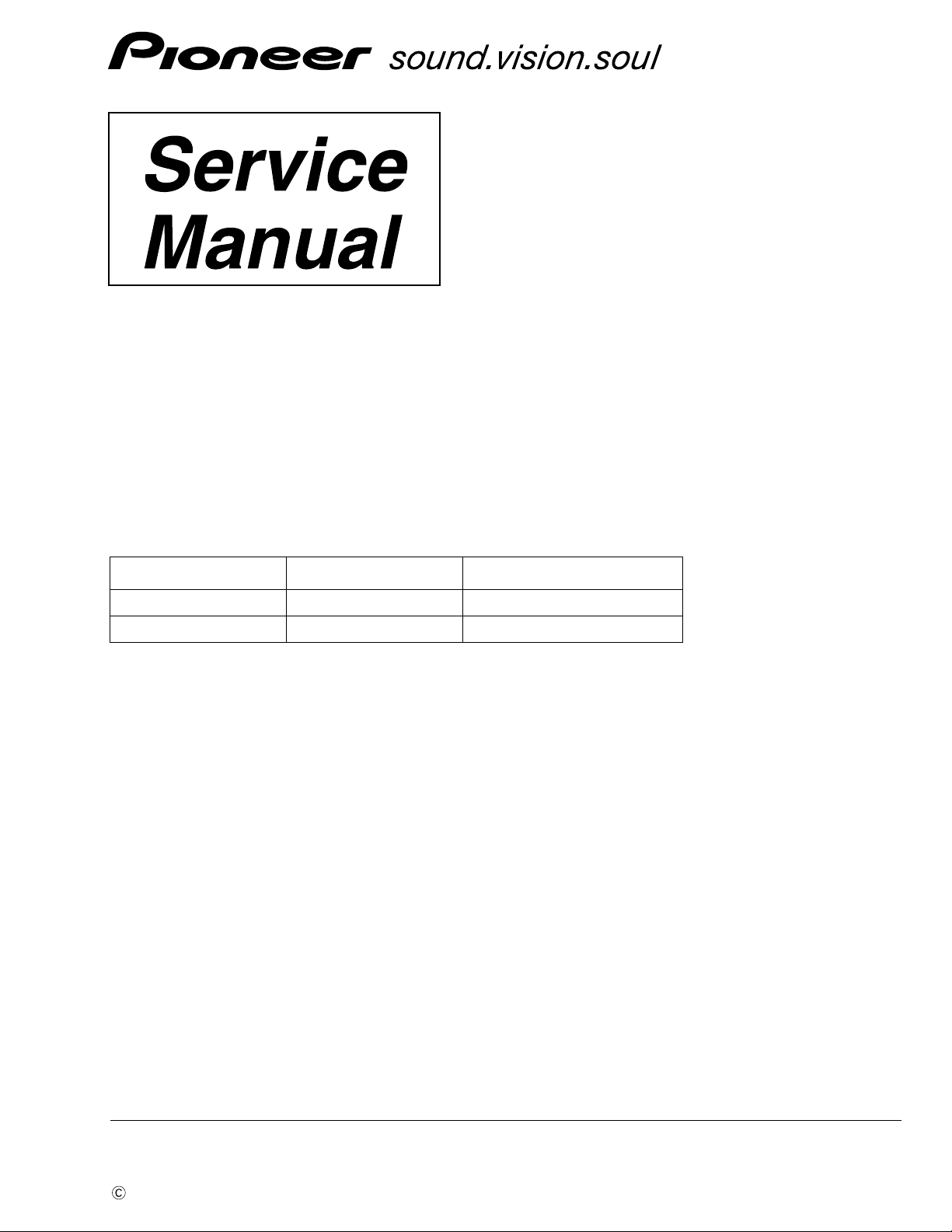
1.1 Analog Block (MN2DS09AAUB:IC1501)
An analog block becomes the following functions.
1.Standard power supply circuit
2.The servo system/ The DPD signal processing system circuit
Gain change amplifier an Low pass filter(LPF)
3.RF signal processing system circuit
RF addition circuit , Inline circuit and Variable Gain Amplifire(VGA) circuit
4.Laser power control (LPC) circuit
C
5.The A/D converter for servo (10bit, 5bit-4ch) , PWM
1.1.1 APC Circuit
The optical output for the laser diode (LD) has large minus temperature characteristics. Therefore, the constant
optical output cannot be obtained when LD is driven by the constant current. APC circuit controls the electric
current so as to provide constant output at the monitor diode (MD). MN2DS09AAUB contain two
types of APC circuits, one for DVD and another for CD. The LD electric current for DVD (CD) can be obtained by
dividing the voltage measurements between DVDLD1 (CDLD1) and 5V by 6 Ω (1.5 Ω x 4=6 Ω ). For DVD (CD),
the results are approx. 50 mA (45 mA).
The potential difference between DVDLD1(CDLD1) and 5 V is set to approx. 300 mV (270 mV).
D
IC1501
CDLPCPOWON
DVDLPCPOWON
5 bit DAC
E
LPCOFS
[4.0]
LPCADJMODE
-
amp1
+
Standard voltage
LPCPW[3.0]
-
amp2
+
DVD : 180 mV
CD : 170 mV
126
125
124
123
LPCO2
LPC2
LPCO1
LPC1
+5 V
+5 V
1.5 Ω 1.5 Ω 1.5 Ω 1.5 Ω
+
1.5 Ω 1.5 Ω 1.5 Ω 1.5 Ω
+
+
CDLD0
DVDLD0
CDLD1
DVDLD1
CN1101
24
5
25
15
78 LD
78 MD
65 LD
65 MD
CDLDDVD
LD
PU Unit
+5 V
MD
F
1234
CX-31832
Page 3
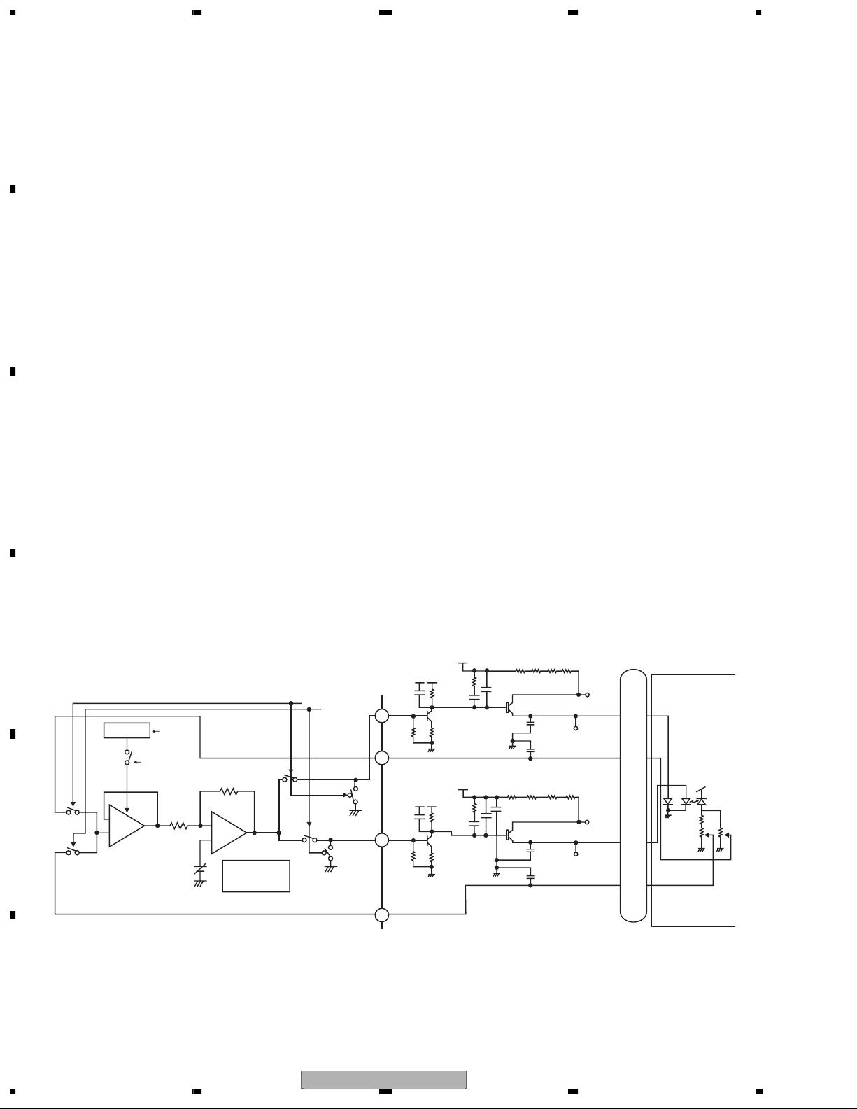
1.1.2 FE Generation Circuit
Focus Error (FE) Generation Circuit
In IC1501 inside, the AD translation of the signals RF1 and RF2 from PU is carried out, and they are taken in.
Then, offset cancellation is considered, differential is taken and it is set to FE.
FE = (FE1) - (FE2)
After 10bit ADC
FE2
VIN8
VIN7
12
11
VIN78
OFS[1:0]
VIN78 G
[1:0]
FE1
CN1101
LPF
Fc=
50 kHz
Selector
Buffer
amplifier
ADC drive amplifier
MAX:2 V[P-P]
G=6/ 7.5/ 9/
10.5/ 12/13.5/
15/ 16.5/ 17/
19.5 dB
10 bit
ADC
0 - AVDD
64 step
GAVIN5
G = 3/9 dB
Pvin7ofs
Dfepsv
1+ Pfbal0,1 / 0x0100
+
-
Pfe_g
FE1
FE
FE2
+
+
GAVIN[4:0]
LPF
Fc=
50 kHz
offset adj.
6 bit DAC
OFFVIN[5:0]
Pvin8ofs
Dfemsv
+
+
1- Pfbal0,1 / 0x0100
134
133
Offset is set up so that it may be settled in
input D range of 10 bit ADC
at the time of Max:2 V[P-P] typ:1.6 V[P-P].
Input D range
max 0-3.3 V
(It is dependent on
power supply voltage)
5678
A
B
C
D
CX-3183
56
E
F
7
8
3
Page 4
1234
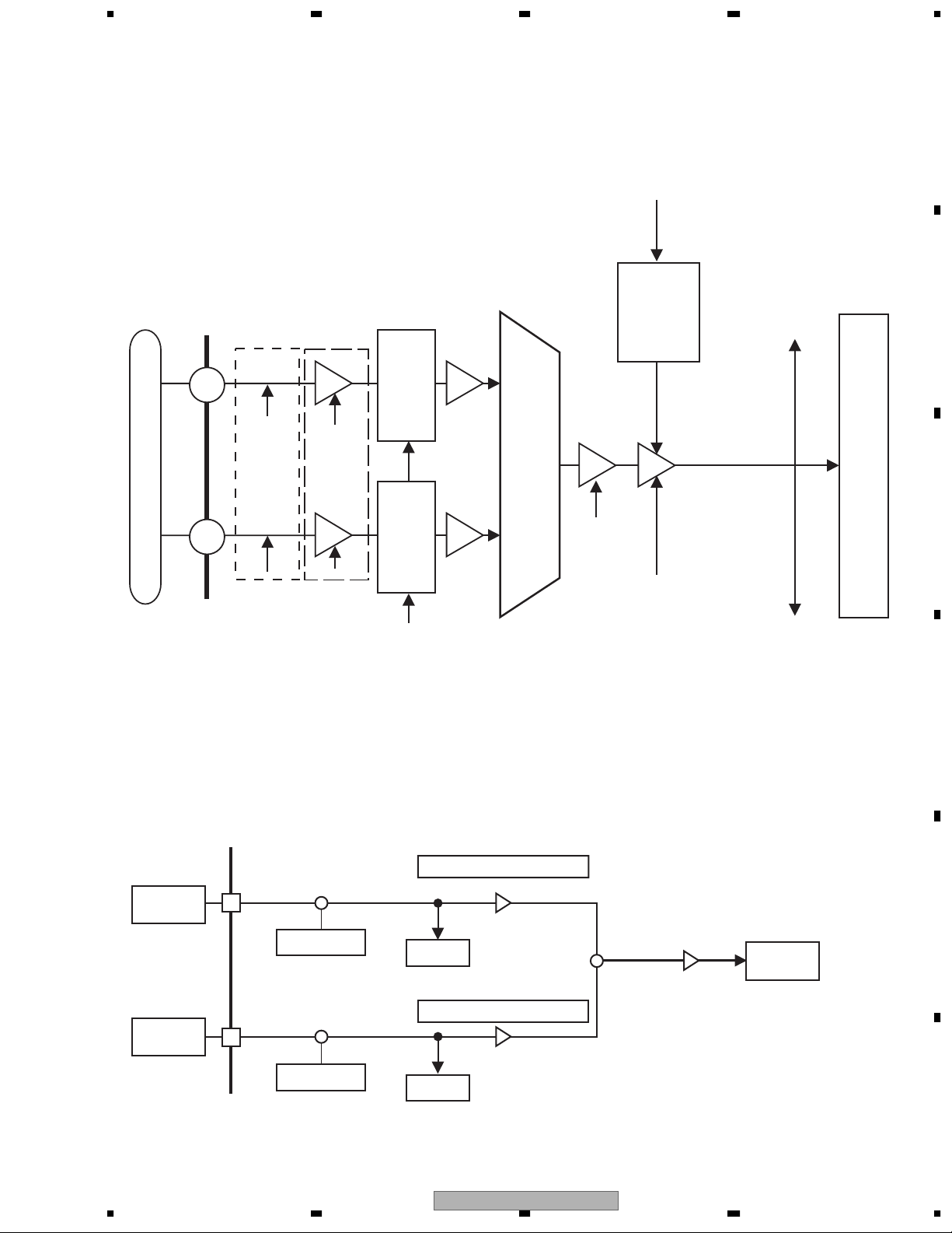
1.1.3 TE Generation Circuit
Trackings Error (TE) Generation Circuit
A
For DVD, TE is generated, with the application of a phase contrast method, from the phase difference of (B2+B4)
and (B1+B3). For CD, TE is generated, with the application of a 3-beam method, by sending the signal to the
variable amp set for the tracking offset adjustment via outer-attached resistance and then by AD-converting it to
make the formula of TE=A
DVD (TE from phase difference)
CN1101
-
C.
115
116
118
117
B
C
B
A
D
C
7
VIN1RF
8
VIN2RF
VIN3RF
11
VIN4RF
9
VIN1RFOUT
VIN2RFOUT
VIN3RFOUT
VIN4RFOUT
LPF
11.3 M/5.7 MHz
LPF
11.3 M/5.7 MHz
LPF
11.3 M/5.7 MHz
LPF
11.3 M/5.7 MHz
HPF
100 kHz
HPF
100 kHz
HPF
100 kHz
HPF
100 kHz
OFFVIN[5:0]
CD (3-beam TE)
D
offset adj.
6 bit DAC
DPDOUT1
DPDOUT2
DPDOUT3
DPDOUT4
0 - AVDD
64 step
5 bit
ADC
5 bit
ADC
DPD
5 bit
ADC
5 bit
ADC
Input D range
max 0-3.3 V
(It is dependent on
power supply voltage)
TE
VIN10
F+H
_G+H
E
E+G
_F+H
CN1101
F
21
22
VIN9
134
133
VIN78
OFS[1:0]
VIN78 G
[1:0]
LPF
Fc=
50 kHz
LPF
Fc=
50 kHz
Selector
Buffer
amplifier
GAVIN5
G = 3/9 dB
ADC drive amplifier
MAX:
2 V[P-P]
G=6/ 7.5/ 9/
10.5/ 12/13.5/
15/ 16.5/ 17/
19.5 dB
GAVIN[4:0]
Offset is set up so that it may be settled in
input D range of 10 bit ADC
at the time of Max:2 V[P-P] typ:1.6 V[P-P].
10 bit
ADC
CX-31834
1234
Page 5
After 10bit ADC
Pvin9ofs
Dtepsv
1+ Ptbal0,1 / 0x0100
+
-
Pfe_g
E+G_E+F
TE
F+H_G+H
+
+
Pvin10ofs
Dtemsv
+
+
1- Ptbal0,1 / 0x0100
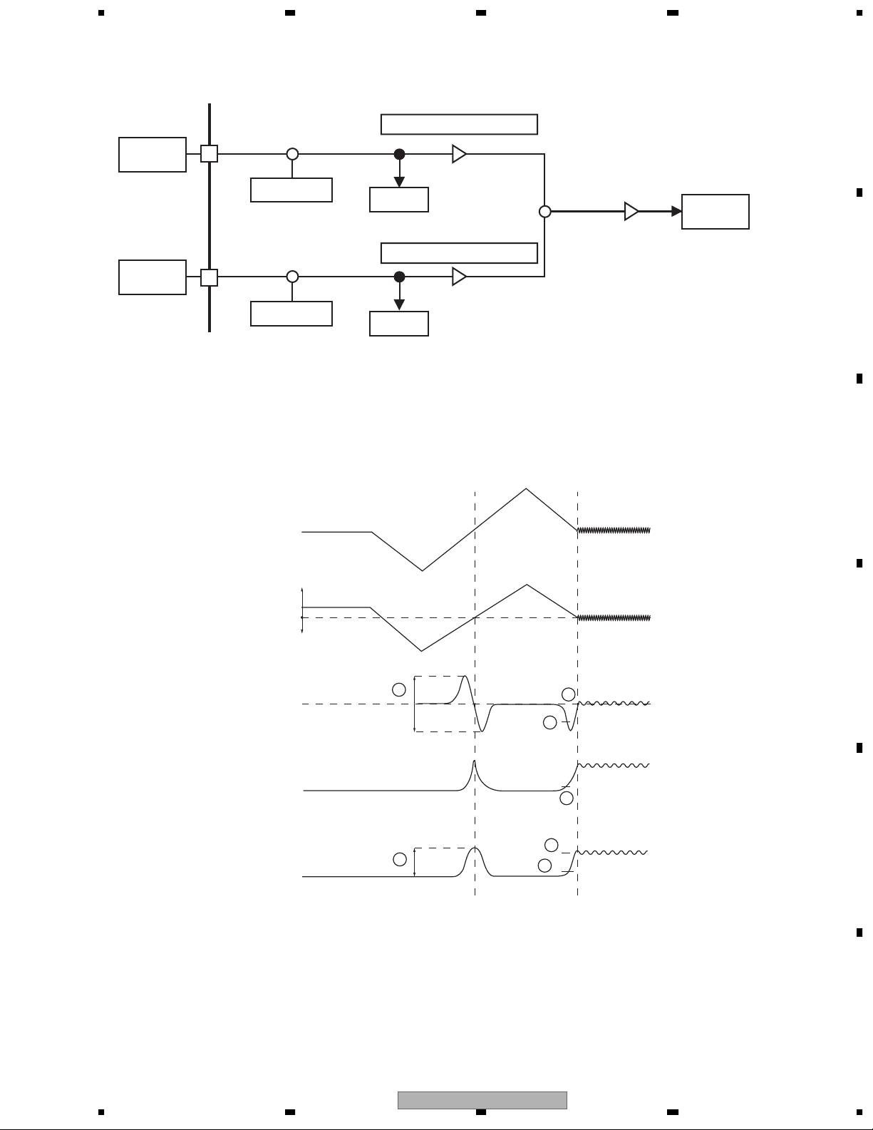
1.2 Servo Block (MN2DS09AAUB:IC1501)
Servo block performs focus, tracking, servo control for traverse, spindle motor control and seek control.
1.2.1 Focus Close
3
6
7
4
5
1
2
Far from disc
Close to disc
Lens
VHALF
Focal point
FE
RFENV
AS
FODRV
5678
A
B
C
D
E
F
56
CX-3183
7
8
5
Page 6

1234
After issuing the focus close command, the following processes are taken for both DVD and CD.
A
1. Measure and optimize signal levels
First drive PU lens far from the disc and then drive closer to the disc. At the focal point met in the process of
this move, measure signal levels of FE, AS and RFENV respectively, and optimize their levels for FE and AS
(1 & 2 in the above figure).
2. Focus closing
Next, drive the lens far from the disc again to detect the closing levels of FE and AS.
Then activate focus loop filter for closing focus (3 6).
3. Check closing
Check the closing with signal levels of AS and RFENV (6 & 7).
Focus search in test mode can check the signal levels and focus drive voltages for FE, AS and RFEV.
B
C
1.2.2 Tracking Close
After issuing the tracking close command, the following processes are taken for both DVD and CD
1. Tracking brake
Measure one half cycle of the tracking cross and if the cycle is within the range of designation, output the brake
pals.
Output direction of brake pals is determined by the phase relations of OFTR and TKC (TE's binarization) signals.
After confirming that the swing of lens against disc is controlled, the brake stops and the closing begins. If the
closing condition is not met within 10msec. after outputting brake, the brake stops and the closing begins.
2. Tracking closing
Process the tracking drive hold with OFTR signal.
3. Check closing
Check whether or not the track jump does not exceed the designated number within the designated term.
Closing check will be time-out at 20msec. Retry using a command from the microcomputer.
1.2.3 Track Jump
The system selects from three types of methods; i.e. interval jump, multi jump and traverse seek,
according to the target number of moving tracks.
1. Interval Jump
The detailed seek is capable due to the execution of repetitive one-track jumps.
It is used when approaching to the target track or seek-operating to an adjacent track.
2. Multi Jump
It counts both edges of the track cross signal TKC and moves for designated number of track counts.
D
3. Traverse Seek
It controls the movement speed by measuring the time of the track cross signal TKC and manages the
vibration of pickup generated upon movement to the minimum.
Types of target number of moving jumps illustrating the jump switch setting for both DVD and CD
DVD
1-10 Interval Jump
11-100 Multi Jump
101-500 Combination of Multi Jump and Interval Jump
Over 501 Traverse Seek
The waveforms of track jumps are shown in the next page.
E
F
CX-31836
1234
CD
1-10 Interval Jump
11-32 Multi Jump
33-500 Combination of Multi Jump and Interval Jump
Over 501 Traverse Seek
Page 7
5678
Tracking-on process
TE
TKC
OFTR
TRDRV
Tracking brake
Tracking on
CLPTM
TROK_TM
Drive hold by OFTR
A
Tracking failure
detaction
B
C
V1 V2 V3
Ts
V2=V1 X TKCLP:L/256
V3=V2 X TKCLP:L/256
#In this case,
int TKCLP:L=0
V2=0
V4 V5 V6
Ts
V5=V4 X TKCLP:H/256
V6=V5 X TKCLP:H/256
D
E
56
CX-3183
F
7
8
7
Page 8
1234
Interval Jump (1 Track)
Outer Jump Inner Jump
A
TE
TD
B
Multi Jump (32 Track)
Outer Jump Inner Jump
TE
TD
C
Traverse Seek (501 Track)
Outer Jump Inner Jump
TE
D
TD
CO
Traverse Seek (5000 Track)
Outer Jump Inner Jump
E
TE
TD
CO
F
CX-31838
1234
Page 9
5678
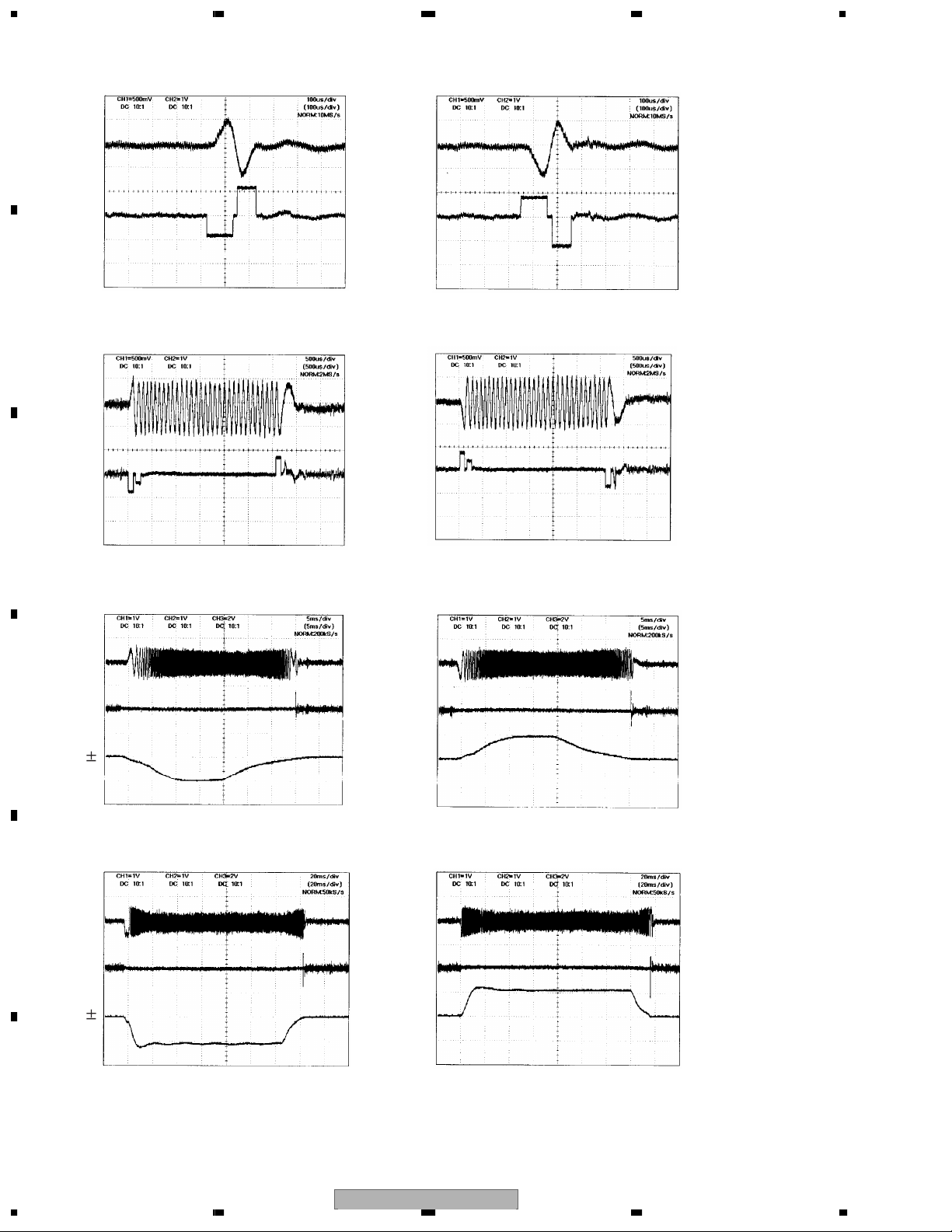
1.2.4 Focus Jump
Focus jump is a function corresponding to the single-sided or both-sided two-layers.
Seen from the object lens, a forward layer is called 0 Layer (L0) and a farther one is called 1 Layer (L1).
A
(1 Layer)
(0 Layer)
L1
L0
object lens
The waveforms of focus jump are shown below.
The waveforms of focus jump
L0 L1
FE
A
B
FD
L1
L0
L1 L0
L0 L1
B C
A D
D
C
L1 L0
B
C
The flow of focus jump is shown below
1. Open tracking at the layer during play.
2. Issue a command to execute jump to the target layer.
3. At the jumped layer, replay by closing the tracking.
Also, the processes when issuing a jump command are as follows
1. Accelerate the lens to the target layer until FE signal detects the acceleration completion level for focus jump.
However, if the time of acceleration time-out reaches before detecting the acceleration completion level,
the acceleration will compulsively stop.
2. Move lens with inertia instead of outputting the drive voltage until FE signal detects the deceleration initiation
level.
3. Decelerate lens for the duration from detection of the deceleration initiation level to the deceleration
completion level.
However, if the time of deceleration time-out reaches before detecting the deceleration completion level,
the deceleration will compulsively stop.
1.3 Automatic Adjustment Function
This system totally automates the circuit adjustments.
The details of automatic adjustments are explained respectively as follows:
1.3.1 VIN7,VIN8,VIN9 and VIN10 Offset Cancel
Each of analog signals for VIN7, VIN8, VIN9 and VIN10 generated at FEP is converted into a digital signal by A/D
converter inside servo block. Offset cancel is a function to cancel the input offset of A/D converter when the power is on.
1.3.2 VCO Gain Adjustment (VARI Adjustment)
It has a function to absorb dispersion of VCO gains among LSI solid by learning and to automatically adjust
VCO gains for the constant allocation. Lock VCO to standard frequency for study,
read Frequency Control Value (FCNT), and then adjust VARI register so that the value becomes
equivalent to the target FCNT value.
D
E
56
CX-3183
F
7
8
9
Page 10

1234
1.3.3 FE Normalization Adjustment
After A/D-converting FE signal level at servo block which was measured at focus close, adjust it to 190LSB at
A
the digital equalizer input stage.
1.3.4 Tracking Balance (TBAL) Adjustment
By applying Newton-Raphson method, search for a balanced point at which DC offset becomes 0 by vibrating
lens toward track direction at the time of the focus close and the tracking open.
1.3.5 Tracking Error Amplitude Learning
After vibrating lens toward track direction at the time of the focus close and the tracking open,
the Tracking Error
amplitude level, adjust it to 190LSB at the digital equalizer input stage
1.3.6 Focus Balance (FBAL) Adjustment
Adjust the focus position so that RFENV becomes maximum at the tracking close.
1.3.7 Focus Gain Adjustment and Tracking Gain Adjustment
B
Insert disturbance to servo loop at the tracking close and adjust to a target gain intersection.
1.3.8 AS Normalization Adjustment
After measuring AS signal levels for the designated number of samplings at the tracking close,
the precise adjustment is made to set 64LSB at the digital equalizer input stage.
All automatic adjustments can be confirmed by indicating their results at test mode.
List of Automatic Adjustment Coefficients
States
Power On
C
D
F Close
F Close (after TBAL)
T Close
Coefficients
VIN7 Offset
VIN8 Offset
VIN9 Offset
VIN10 Offset
FE MAX
FE MIN
AS MAX
FE Normalization
TE MAX
TE MIN
TE Normalization
F Gain
T Gain
AS Normalization
06B7 08CD
06B7 08CD
0E48 36CD
C933 F1B8
0981 3384
01BB 06A7
1A90 4D58
B2A8 E570
0145 02E9
0100 0400
0100 0400
013E 06BC
DVD
06E1 08A3
06E1 08A3
06B7 08CD
06B7 08CD
13A5 469A
B966 EC5B
0A23 3600
0158 04D3
0337 381A
C7E6 FCC9
01B1 1D85
012F 0650
CD
Note: Coefficients are indicated in hexadecimal numbers.
All figures describe specifications at the production line.
Disc applies DVD
-
REF-A1 for DVD and TCD-782 for CD.
1.4 CIRC Block (MN2DS09AAUB:IC1501)
CIRC block contains digital signal processing function for CD-DA and CD-ROM (EFM demodulation and error
correction), digital servo processing for spindle motor.
E
F
1.5 DRC Block (MN2DS09AAUB:IC1501)
Digital Read Channel (DRC) provides A/D converter, adaptive equalization, bit-a-bit detector, digital PLL circuit,
Digital equalizer(DEQ),RISC interface and peripheral circuits for reading signals of optical disks.
CX-318310
1234
Page 11

5678
2. CIRCUIT DESCRIPTIONS(BE PART)
2.1 POWER SUPPLY MAP
HOST
Power Supply
VD8(Reg)
8V+/-0.4V
VD8V
Mecha inside
Power Supply
5V Reg(VCC5)
5.0v +/-0.1v
IC1004
NJM2880U05
5V Reg(AVCC5)
5.0v +/-0.1v
IC1005
S-L2980A50MC-C7J
Supply
IC
Pick Up Unit
CGY4700
LD
Photo IC
ADAC+LPF
IC1821 PCM1753DBQ
IC1822 NJM2140R
IC1823 NJM2100V
Video circuit
A
B
VD8
8V+/-0.4V
VDD5
5V+/-0.4V
3.3
DC/DC(VCC33)
3.21V ---> 3.41V
2ch DC/DC Converter
IC1003
BD9851EFV
Disc detect LED
C
1chip Driver
IC1201
BD7967EFS
1chip Driver(8V)
1chip Driver(5V)
D
SDRAM
IC1481
EDS1232AATA-75-E
Flash-ROM
IC1402
S99AL016DBT1
Other
E
DVD LSI
IC1501
MN2DS09AAUB
1.2
DC/DC(VCC12)
1.19V ---> 1.25V
SRVDD
3V+/-0.15V
CX-3183
56
DVD1chip(3.3V)
DVD1chip(1.2V)
SRAM
IC1452
M5M5V216ATP-70HI
7
F
11
8
Page 12

1234
A
IC1821
Audio-DAC
PCM1753DBQ
B
SCK
16pin
R1523
C
L1503
CTF1387 27 Ω
DACCLK
33.8688 MHz or 36.864 MHz
D
E
166pin
DACCLK
OSCI
162pin
R1531
1 MΩ
X1501
CSS1697
C1519
7pF or 8 pF
27 MHz
IC1501
DVD-LSI
OSCO
163pin
1 kΩ
R1532
MN2DS09AAUB
[Outline]
Connecting 27MHz crystal resonator to the DVD-LSI (IC1501) will generate and provide DACCLK for the external connection of Audio-DAC
at the clock generator inside DVD-LSI other than the clock used inside LSI.
F
2.2 Clock Circuit
CX-318312
1234
8 pF
C1518
Page 13

5678
2.3 Audio Circuit
[Outline]
2.3.1 Analog Audio Signal
The serial 3-line digital output+DACCLK [digital serial audio data] that outputs from DVD-LSI (IC1501) is converted to
the analog audio signal by Audio-DAC (IC1821) for an output from HOST IF (CN1901).
Also, the analog MUTE signal is simultaneously output from DVD-LSI (IC1501) via HOST IF (CN1901).
2.3.2 Digital Audio Signal (IEC60958/IEC61937)
The digital audio signal (IEC60958/IEC61937) that outputs from DVD-LSI (IC1501) is generated
via Multi-ch/Ripping IF (CN1851).
2.3.3 Digital Multi-channel Audio Serial Signal
The serial 6-line output that outputs from DVD-LSI (IC1501) is generated via Multi-ch/Ripping IF (CN1851).
2.3.4 CD-DA Ripping Signal
The serial 3-line digital output+SUB-CODE signal that outputs from DVD-LSI (IC1501) is generated at quadruple
speed via Multi-ch/Ripping IF (CN1851).
[Analog audio signal]
MS4 Mechanism Module
AVCC5
AVCC5
27PIN:Analog
Rch29PIN:Analog
Lch26,28,30PIN:Audio
GND20PIN:AMUTE
Audio
DAC
PCM1753
fc=88 kHz
820ohm
470pF
4.7uF
100 kohm
CN1901
Audio circuit
47 kohm
or more
A
B
C
AGND
IC1821
AVCC5
470pF
820 ohm
100 kohm
4.7 µF
AMUTE
Audio
MUTE
CIRCUIT
GND
47 kohm
or more
D
E
56
CX-3183
F
7
8
13
Page 14

1234
[Digital Audio Signal]
A
166pin
168pin
167pin
169pin
173pin
DACCLK
BCK
LRCK
ADOUT3
IC1821
ADAC
(Stereo)
IECOUT
TC74VHC125FTx2
IC1851
BCK
B
171pin
170pin
172pin
ADOUT0
ADOUT1
ADOUT2
DATAOUT
DVD_LSI
IC1501
CN1851
LRCK
C
24PIN Multich Output(Digital)
IC1852
95pin
97pin
IC1853
80pin
BMUTE
MCKENA
Pull-up
RIPP
"H"output
EMPH
[CD-DA Ripping Signal]
D
E
F
DVD_LSI
IC1501
173pin
168pin
172pin
171pin
170pin
169pin
167pin
190pin
97pin
80pin
TC74VHC125FTx2
IC1851
NCLDCK
DATAOUT
IC1852
MCKENA
IC1853
"L"output
IPFLAG
BCK
SUBC
BLKCK
LRCK
SBCK
Pull-up
RIPP
EMPH
CN1851
24PIN Ripping Data & Sub code Output
1234
CX-318314
Page 15

5678
Video Circuit
Composite Video Signal and Component Signal is output from DVD-LSI(IC1501) circuit part.
Output from HOST I/F(CN1901) via Buffer circuit.
A
MS4 MECHANISM MODULE
DVD LSI
(DV3.2)
Video DAC
(CVBS,Y/Pb/Pr)
156pin : CVBS
149pin : Component Y
148pin : Component Cb
147pin : Component Cr
AVCC5
Q1803 : CVBS
Q1801 : Component Y
Q1802 : Component Cb
Q1804 : Component Cr
Zo=75 ohm
CVBS:32Pin
Y:34Pin
Cb(Pb):36Pin
Cr(Pr):38Pin
VIDEO GND
31,33,35,
37,39Pin
VIDEO AMP
(with LPF &
75 ohm DRIVER)
(*1)
B
C
D
56
CX-3183
E
F
7
8
15
Page 16

1234
2.4 SDRAM I/F
A
[Outline]
It is a memory to realize AV decoding function for DVD-LSI (IC1501). It is used for the buffering of stream data before
decoding, the work domain upon decoding, the storage of AV data and output data after decoding and manyother purposes.
SDRAM Interface
*Seen from DVD-LSI
Signal Name Bits I/O
MDQ[31:0] 32 I/O
MA[11:0] 12 O
B
BA[1:0] 2 O
NRAS 1 O
NCAS 1 O
NEW 1 O
NCS 1 O
DQM[0] 1 O
DQM[1] 1 O
DQM[2] 1 O
DQM[3] 1 O
MCK 1 O
C
MCKI 1 I
Description
Data bus for external SDRAM
SDRAM address
SDRAM bank address
RAS signal in SDRAM
CAS signal in SDRAM
Write enable signal in SDRAM
Chip select signal in SDRAM
Mask signal writing lower byte among the lower 2 bytes in SDRAM
Mask signal writing higher byte among the lower 2 bytes in SDRAM
Mask signal writing lower byte among the higher 2 bytes in SDRAM
Mask signal writing higher byte among the higher 2 bytes in SDRAM
Clock input into SDRAM
Clock input for data input from SDRAM
SDRAM Specifications
• Data bus width : 32bit
• Operating frequency : 121.5 MHz
• CAS latency = 3
• 8-word burst transfer
• CAS before RAS refresh (Auto refresh)
D
Configuration of SDRAM Connection
DVD-LSI SDRAM
MDQ[31:0] DQ[31:0]
MA[11:0] A[11:0]
BA[1:0] BA[1:0]
NRAS XRAS
NCAS XCAS
NEW XWE
DQM[3:0] DQM[3:0]
E
NCS XCS
MCK CLK
MCKI
F
CX-318316
1234
Page 17

5678
3. MECHANISM DESCRIPTIONS
Configuration
PU unit
Spindle
motor
A
CRG motor
B
Load motor
C
SW4
8/12 detection lever L
SW6
SW1
D
SW5
(CLAMP SW)
SW2
SW3
8/12 detection lever R
E
F
56
CX-3183
7
8
17
Page 18

1234
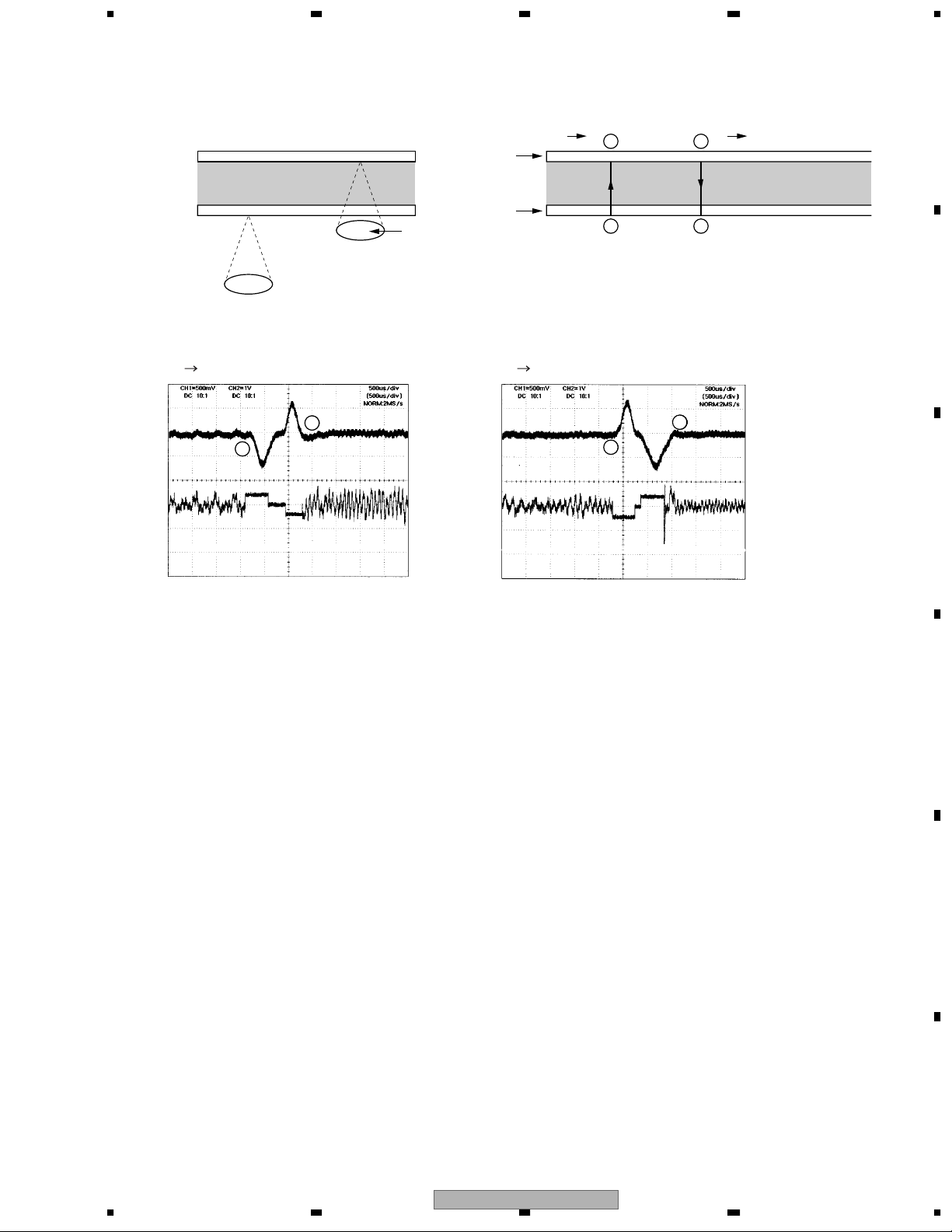
3.1 Disc loading operation
A
1. When a disc is inserted,
from ON to OFF, which triggers the operation of the loading motor.
2. For a 12cm disc, the switch SW3 is turned OFF and SW4 is ON during disc transportation. The microcomputer
senses that a 12cm disc is loaded.
B
the 8/12-detection levers R and L slide. Either of the switches SW1 and SW2 is shifted
C
12 cm disk
3. For an 8cm disc, neither the switch SW3 nor SW4 will be shifted to the above states (SW3: OFF, SW4:ON)
during disc transportation. The operation mode proceeds to the clamp operation. The microcomputer senses that an
8cm disc is loaded.
D
E
8 cm disk
F
1234
CX-318318
Page 19

5678
3.2 Disc centering mechanism
1. With a 12cm disc loaded, the disc pushes both of the lock arms R and L to open the centering arms R and L. Then,
the clamp arm or the stopper of the centering arm R stops the disc for centering. The operation mode
proceeds
to the clamp operation.
A
Centering arm
Clamp arm
12 cm disk latching section
Lock arm
12 cm disk latching section
B
Centering arm
C
2. With an 8cm disc loaded, the disc pushes either of the lock arms R and L. The lock arms R and L are connected
each other via the centering arms R and L. The lock arms R and L will be kept locked unless the disc pushes them
at the same time. Therefore, the lock arm blocks the disc for centering. During disc centering, the disc pushes
out the disc detection arm. When the detection arm completes moving, the disc stops. The operation mode
proceeds to the clamp operation.
8 cm disk latching section
D
E
F
56
CX-3183
7
8
19
Page 20

1234
2.3 Clamp operation
1. When an 8 or 12 cm disc is centered over the spindle, the disc detection arm moves the clamp lever. The loading
A
rack driven by the clamp lever is engaged with the lever driving gear , which triggers the disc clamp operation.
Disc detection arm
Disc positioning section
Clamp lever
Loading rack
B
Load lever R
Clamp switch
C
2. When pressed by the loading rack, the load lever R moves toward the front side, and the roller shaft, which is
connected to the cam of the load lever R, moves downward. The roller shaft is connected to the cam of the cam
ring also. Therefore, the drive of the roller shaft is transferred to the load lever L via the cam ring. The load lever
L moves toward the front side. The load lever cams are released from the three shafts for the CRG chassis unit
and the clamp arm shaft. When the load lever R turns on the clamp switch, the clamp operation ends.
D
CRG chassis
linked with the cam
shaft
Clamp arm shaft
linked with the cam
E
CRG chassis shaft
linked with the cam
CRG chassis
linked with the ca m
2.4 Eject operation
1. When the loading motor turns in reverse, the disc eject operation begins.
2. With a 12cm disc loaded, when the SW4 is shifted from OFF to ON, and then OFF again, the eject operatio n
F
ends.
3. With an 8cm disc loaded, when the SW3 or SW6 is shifted from ON to OFF,and then both switches are turned
ON, the eject operation ends.
CX-318320
1234
shaft
Page 21

5678
4. DISASSEMBLY
- Precautions on handling the mechanism module
1. Hold the upper and main frames.
2. Do not hold the front portion of the upper frame. It is a delicate part.
3. Do not touch the switches on the top panel.
4. Be careful not to catch the flexible cables.
(Fig.1)
A
B
Do not touch here. Do not touch here.
Do not hold this delicate portion.
Fig. 1
- Removing the module pc board (Fig.2 and 3)
1. Set the mechanism to the lock position (disc load standby position).
2. Place the mechanism module upside down.
3. Short the two lands on the pickup flexible cable as shown below.
4. Be sure to disconnect the pickup flexible cable and the SPDL flexible cable from the connectors
to protect them from damages.
5. Remove solder from the load motor leads and clamp SW leads.
6. Loosen the two fixing screws. Lift the position A of the module pc board lightly and move it
in the direction B to remove it. Be careful not to damage the flexible cable C.
7. Disconnect the 8/12 detection flexible-cable from the connector.
Short here.
Fig. 2
Connector
(for pickup flexible cable)
(for 8/12 detection
flexible cable)
C
D
Module pc board
E
Connector
Solder land
(Load motor
leads and clamp SW leads)
56
Connector
(for SPDL flexible cable)
CX-3183
B
A
C
Fig. 3
F
7
8
21
Page 22

1234
- Removing the pickup unit (Fig. 4)
1. Remove the module pc board in accordance with the procedure of "Removing the module pc board.”
A
2. A principal-axis control spring is hung on a CRG chassis.
3. While holding the pickup case, remove the skew screw (main).
4. Lifting the end of the pickup rack, slide the main shaft, and remove the pickup unit.
Notes:
Replacing the pickup unit requires the skew adjustment .
Remove glue from both ends of the main and sub shafts, and skew stud.
Do not reuse the old skew screw . Be sure to use a brand-new skew screw supplied with a new pickup unit.
Fix the locking agents(1401M : produced by THREE BOND) after adjustment.
B
Hang on a position based on a principal-axis control spring.
Skew screw (main)
Main shaft
Pickup unit
C
Principal-axis control spring
Skew screw(Sub)
Skew screw(Sub)
Sub shaft
D
The position of the CRG chassis hung temporarily
Fig. 4
It hangs temporarily It hooks perfectly.
E
F
CX-318322
1234
Page 23

5678
- Removing the spindle motor (Fig.5)
1. Remove the module pc board in accordance with the procedure of "Removing the module pc board."
2. Remove the three fixing screws for the SPDL motor . Be careful not to deform the CRG chassis when replacing
the SPDL motor.
3. After removing the lead of a CRG motor from a hook, it removes from a flexible land.
- Removing the CRG motor assy (Fig.5)
1. Remove the module pc board in accordance with the procedure of "Removing the module pc board.
2. Remove the module pc board in accordance with the procedure of "Removing the spindle motor."
3. Remove the feed screw.
4. Remove the fixing screw , and remove the feed screw holder together with the 2-stage gear .
5. Remove the fixing two screws and CRG motor assy .
Caution:
When replacing the CRG motor assy, be careful not to damage the gears, especially the 2-stage gear that is
very delicate. When lifting the pickup rack to install the motor , be careful not to damage the gear teeth.
When you remove a feed screw, be careful for a feed screw holder not to separate.
”
A
B
Feed screw holder
CRG motor assy
Screw(CRG)
Screw(CRG)
Hook
Feed screw
Pickup rack
Solder land
2-stage gear
Feed holder
Hook
Screw(holder)
Screw(spindle)
Hook
SPDL motor
Screw(spindle)
Screw(spindle)
Fig. 5
- Removing the upper frame assy (Fig. 6)
1. Remove the module pc board in accordance with the procedure of "Removing the module pc board. ”
2. Remove the spring.
3. Remove the four screws and remove the upper frame assy .
Screw
Screw
C
D
Screw
Fig. 6
CX-3183
56
Spring
Upper frame assy
Screw
7
E
F
23
8
Page 24

1234
- Removing the load gear assy (Fig. 7)
1. Remove the module pc board in accordance with the procedure of "Removing the module pc board.”
A
2. Remove the upper frame assy in accordance with the procedure of "Removing the upper frame assy.”
3. Remove the two screws and remove the load gear assy .
Screw
Load gear assy
B
Screw
Fig.
7
C
- Setting the quasi-clamp mode by driving the loading motor (Fig. 8)
1. While driving the loading motor in the clamping direction, pull the clamp lever toward the front side.
2. Even after the clamp lever pushes the loading rack (clamp mode), keep the clamp lever pulled lightly.
Prevent the clamp lever bar ring from coming into the clamp spring. If not, ejection will not be impossible.
3. After the clamp operation ends, stop the operation before the objection of the loading rack touches the load
lever R.
D
(fig. 10)
Clamp lever
Pull toward the front side.
E
8
Fig.
F
CX-318324
1234
Page 25

5678
Clamp lever
bar rin g
A
Clamp spring
B
Prevent the clamp lever bar rin g
from coming into the clamp
spring (the above condition is NG)
Fig. 9
Load lever R
Stop before this
clearance
becomes zero.
C
Loading rack
D
E
56
CX-3183
Fig. 10
7
F
25
8
Page 26

1234
- Setting the quasi-clamp mode manually (Fig. 11)
1. Remove the module pc board in accordance with the procedure of "Removing the module printed circuit board.”
A
2. Remove the upper frame assy in accordance with the procedure of "Removing the upper frame assy .”
3. Remove the load gear assy in accordance with the procedure of "Removing the load gear assy ."
4. While pulling the clamp lever toward the front side, pull the fixed portion of the load lever R toward the front
side
until the mode enters the clamp position.
Clamp lever
B
load lever R forward.
Load lever R
Fig. 11
Pull this portion of the
C
- Removing the load motor assy (Fig. 12)
1. Remove the module pc board in accordance with the procedure of "Removing the module printed circuit board. ”
2. Remove the upper frame assy in accordance with the procedure of "Removing the upper frame assy.”
3. Remove the load gear assy in accordance with the procedure of "Removing the load gear assy ."
4. Enter the quasi-clamp mode in accordance with the procedure of “Setting the quasi-clamp mode manually .”
5. Remove the screw . Slide the load motor assy to pull it out .
D
E
Screw
Slide to remove.
Fig. 12
F
1234
CX-318326
Page 27

5678
- Removing the CRG assy (Fig. 13)
1. Enter the quasi-clamp mode in accordance with the procedure of “Setting the quasi-clamp mode by driving
loading motor .”
the
2. Remove the module pc board in accordance with the procedure of "Removing the module pc board. ”
3. Remove the upper frame assy in accordance with the procedure of "Removing the upper frame assy .”
4. Remove the four springs.
5. Lift the CRG assy until the shafts come from the dampers, and then remove it.
- Removing the disc guide assy (Fig. 13)
1. Enter the quasi-clamp mode in accordance with the procedure of “Setting the quasi-clamp mode by driving
loading motor .”
the
2. Remove the module pc board in accordance with the procedure of "Removing the module pc board. ”
3. Remove the upper frame assy in accordance with the procedure of "Removing the upper frame assy.”
4. Remove the two disc guide springs. While lifting the disc guide and keeping the lifting angle around 45
degrees,
slide the guide in the left side to remove it.
A
B
Spring
Disc guide spring
Spring CRG assy
Disc guide
Disc guide spring
Spring
C
D
Fig. 13
56
CX-3183
E
F
7
8
27
Page 28

1234
- Removing the roller assy (Fig. 14)
1. Remove the module pc board in accordance with the procedure of "Removing the module pc board.”
A
2. Remove the upper frame assy in accordance with the procedure of "Removing the upper frame assy.”
3. Remove the tension spring.
4. Remove the load gear assy in accordance with the procedure of "Removing the load gear assy."
5. Enter the quasi-clamp mode in accordance with the procedure of “Setting the quasi-clamp mode manually.”
6. Remove the disc guide assy in accordance with the procedure of “Removing the disc guide assy.”
7. Remove the CRG assy in accordance with the steps 4 and 5 in the procedure of “Removing the CRG assy .”
8. By pushing the fixed portion of the load lever R, move the load lever R to the rear side completely.
9. Remove the load levers R and L. Unhook the end of the roller arm spring R from the load lever R.
10. While lifting the roller assy to the highest position, slide it to the right side. Lightly bend the whole slot guide by
B
pushing the ends with your fingers and remove the roller assy .
Caution : A shutter is not changed when removing Roller Assy.
Load lever R
C
Move to the rear
side
Roller arm spring R
Roller arm spring L
Shutter
D
Roller assy
Tension spring
Shutter
Fig. 14
E
F
CX-318328
1234
Page 29

5678
- Removing the dampers (Fig. 15)
1. Enter the quasi-clamp mode in accordance with the procedure of “Setting the quasi-clamp mode by driving
the
loading motor .”
2. Remove the module pc board in accordance with the procedure of "Removing the module pc board. ”
3. Remove the upper frame assy in accordance with the procedure of "Removing the upper frame assy.”
4. Remove the three springs.
5. Remove the CRG assy in accordance with the steps 4 and 5 in the procedure of "Removing the CRG assy.”
6. Release each of the three dampers from the clinches as follows:
6.1 By using a pair of pliers, hold the portion A and turn them in the direction B. While making a gap in the portion
C, release the damper from the clinches.
6.2 Insert a flat-type screwdriver into the portion D. Slightly raise the plate and release the damper from the
clinches.
7. Remove the CRG motor assy in accordance with the steps 3 through 5 in the procedure of "Removing the CRG
motor assy .”
8. Remove the dampers.
A
B
C
A
C
B
D
Fig. 15
D
56
CX-3183
E
F
7
8
29
 Loading...