Page 1
PIONEER CORPORATION 4-1, Meguro 1-Chome, Meguro-ku, Tokyo 153-8654, Japan
PIONEER ELECTRONICS (USA) INC. P.O.Box 1760, Long Beach, CA 90801-1760 U.S.A.
PIONEER EUROPE NV Haven 1087 Keetberglaan 1, 9120 Melsele, Belgium
PIONEER ELECTRONICS ASIACENTRE PTE.LTD. 253 Alexandra Road, #04-01, Singapore 159936
C PIONEER CORPORATION 2002
K-ZZA. JAN. 2002 Printed in Japan
ORDER NO.
CRT2820
Model Service Manual CD Mechanism Module
DEH-P740MP/XN/UC CRT2783 CXK5555
DEH-P7400MP/XN/UC
DEH-P7450MP/XN/ES
DEH-P7400MP/XN/EW CRT2784
CD MECHANISM MODULE
CX-3007
- This service manual describes the operation of the CD mechanism module incorporated in models
listed in the table below.
- When performing repairs use this manual together with the specific manual for model under repair.
CONTENTS
1. CIRCUIT DESCRIPTIONS ...........................................2
2. MECHANISM DESCRIPTIONS.................................18
3. DISASSEMBLY .........................................................20
Page 2
2
C X-3007
1. CIRCUIT DESCRIPTIONS
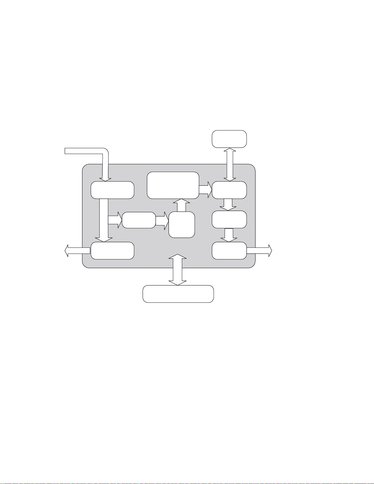
Recently, most CD LSI's have included DAC, RF amplifier and other peripheral circuits, as well as the core circuit DSP.
This series of mechanisms employ a multi-task LSI UPD63760GJ, which has CD-ROM decoder and MP3 decoder in
addition to the CD block as shown in the Fig.1.0.1. This enables to reproduce a CD-ROM where MP3 data is recorded.
Plus, in this lineup, there are WMA supported models available where WMA decoder UPD61002GC is added.
CXK5555 --- WMA non-supported
CXK5556 and CXK5557 --- WMA supported
Fig.1.0.1 Block diagram of CD LSI UPD63760GJ
DRAM
A - F
RF
AMPLIFIER
EFM
DRIVE
OUTPUT
DIGITAL
SERVO
CD-ROM
DECODER
SIGNAL
PROCESSOR
UCOM
BMC
MP3
DECODER
AUDIO
OUTPUT
DAC
UPD63760GJ
Page 3
3
C X-3007
1.1 PREAMPLIFIER BLOCK (UPD63760GJ: IC201)
In the preamplifier block, the pickup output signals are processed to generate signals that are used for the next-stage
blocks: the servo block, demodulator, and control.
After I/V-converted by the preamplifier with built-in photo detectors (inside the pickup), the signals are applied to the
preamplifier block in the CD LSI UPD63760GJ (IC201). After added by the RF amplifier in this block, these signals are
used to produce necessary signals such as RF, FE, TE, and TE zero-cross signals.
The CD LSI employs a single power supply system of + 3.3V. Therefore, the REFO (1.65V) is used as the reference
voltage both for this CD LSI and the pickup. The LSI produces the REFO signal by using the REFOUT via the buffer
amplifier and outputs from the pin 131. All the measurements should be made based on this REFO.
Caution: Be careful not to short the REFO and GRD when measuring.
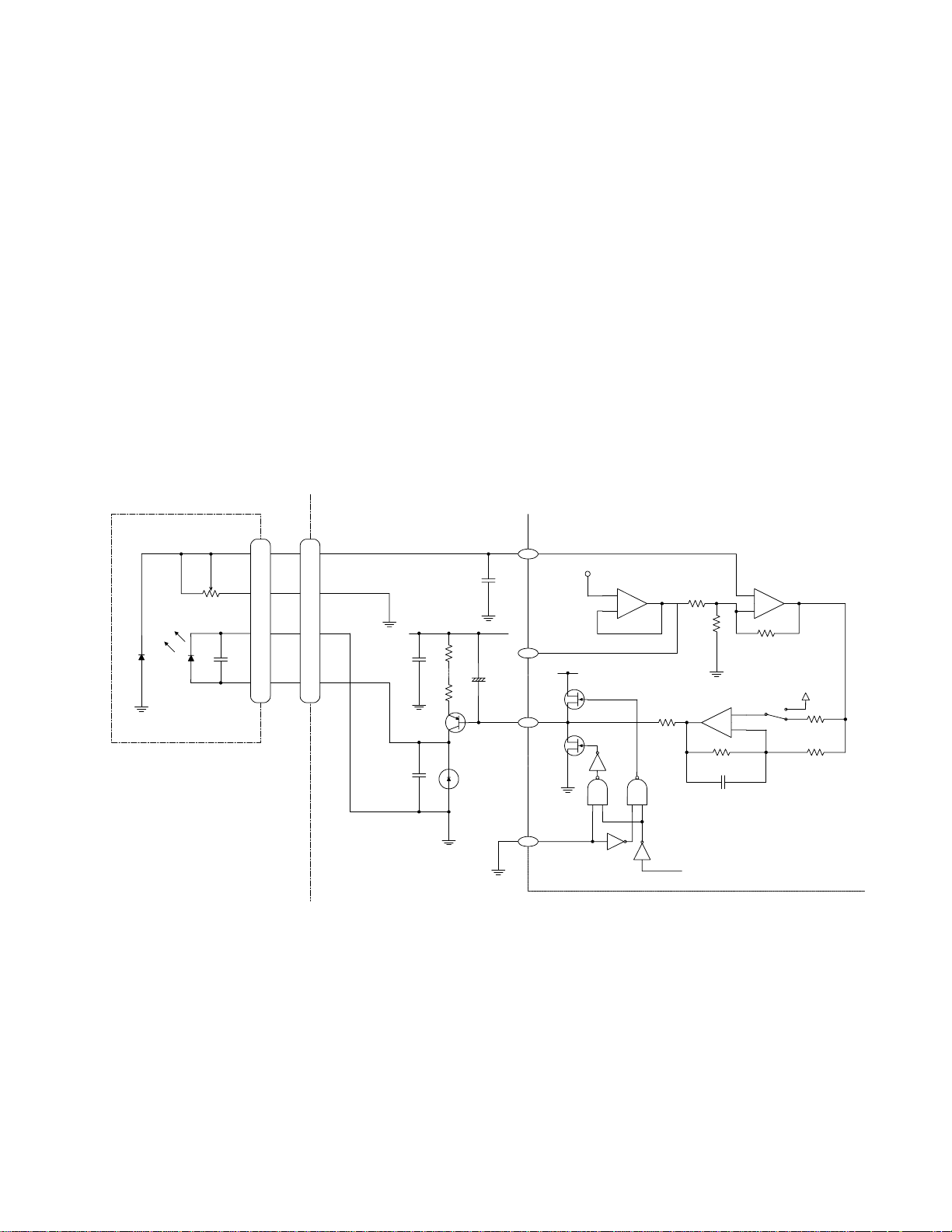
1.1.1 APC (Automatic Power Control)
A laser diode has extremely negative temperature characteristics in optical output at constant-current drive. To keep
the output constant, the LD current is controlled by monitor diodes. This is called the APC circuit. The LD current is
calculated at about 30mA, which is the voltage between LD1 and V3R3D divided by 7.5 (ohms).
Fig. 1.1.1 APC
PICKUP UNIT
MD
VR
LD-
LD+
UNIT
5
7
15
14 14
141
5
R001
7
15
1R5 x 5
R1 R1
100/16
+
2SB1132
1SS355
PD
140
LDREGO
142
LD
143
PN
UPD63760GJ
REG 1R25V
+
-
1K
LDS
6R5K
1K
+
-
110K
+
-
6R5K
Vref
APN
100K
100K
3P
Page 4
4
C X-3007
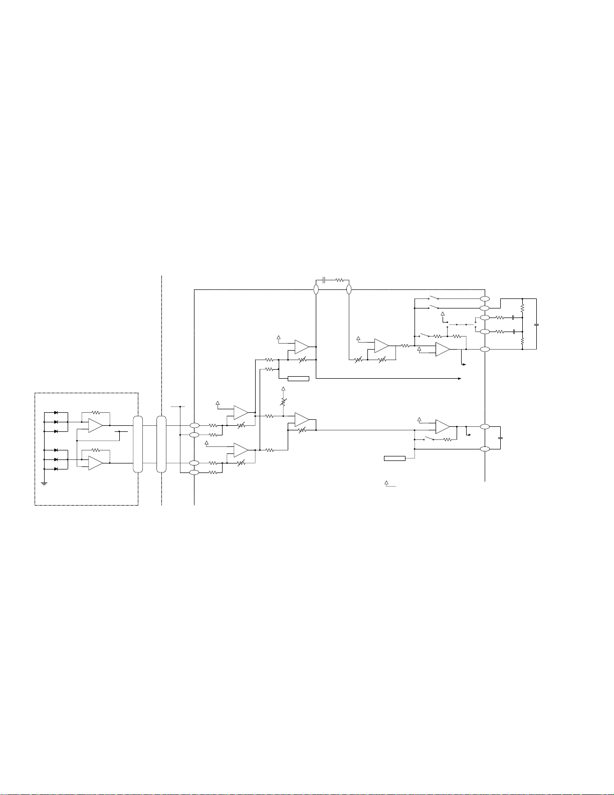
1.1.2 RF and RFAGC amplifiers
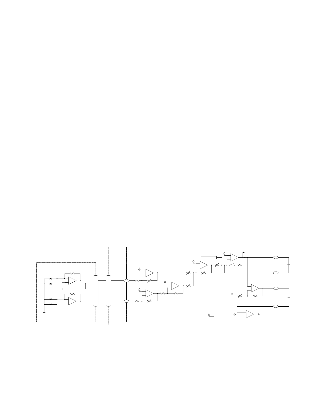
The photo-detector outputs (A + C) and (B + D) are added, amplified, and equalized inside this LSI, and then provided
as the RF signal from the RFI terminal. The RF signal can be used for eye-pattern check.
The low frequency component of the RFO voltage is:
RFO = (A + B + C + D) x 2
The RFO is used for the FOK generation circuit and RF offset adjustment circuit.
The RFI output from the pin 118 is A/C-coupled outside this LSI, and returned to the pin 117 of this LSI. The signal is
amplified in the RFAGC amplifier to obtain the RFAGC signal. This LSI is equipped with the RFAGC auto-adjustment
function as explained below. This function automatically controls the RFO level to keep at 1.5V by switching the
feedback gain for the RFAGC amplifier.
The RFO signal is also used for the EFM, DFCT, MIRR, and RFAGC auto-adjustment circuits.
Fig. 1.1.2 RF/AGC/FE
PICKUP UNIT
P3
P7
P9
P2
P4
P8
VREF
A+C
B+C
RFO
18K
117
AGCI
20K 11R2K
+
-
RFOFF SETTING
7R05K
VREF
10K 10K
+
DEFECT/
A3T DETECTION
RFOK
GENERATION
+
-
RF2-
RF-
EQ2
EQ1
AGCO
FEO
FE A/D
FE-
121
122
119
120
116
134
133
330
1R8K
R01
18P
27P
10K
3P
10K
UNIT
VREF
13
13
6
6
A
C
D
B
UPD63760GJ
124
10k
125
10k
127
10K
126
10K
+
-
+
-
8R8K
8R8K
15R2K
61R0K
61R0K
15R2K
R2
118
+
-
35K
RFOFF SETTING
+
-
111K
Page 5
5
C X-3007
1.1.3 Focus error amplifier
The photo-detector outputs (A + C) and (B + D) are applied to the differential amplifier and the error amplifier to obtain
the (A + C - B - D) signal, which is then provided from the pin 91 as the FE signal.
The low frequency component of the FE voltage is:
FE = (A + C - B - D) x 8.8/10k x 111k/61k x 160k/72k
= (A + C - B - D) x 3.5
The FE output shows 1.5Vp-p S-shaped curve based on the REFO. For the next-stage amplifiers, the cutoff frequency
is 14.6kHz.
1.1.4 RFOK
The RFOK circuit generates the RFOK signal, which indicates focus-close timing and focus-close status during the play
mode, and outputs from the pin 53. This signal is shifted to "H" when the focus is closed and during the play mode.
The DC level of the RFI signal is peak-held in the digital block and compared with a certain threshold level to generate
the RFOK signal. Therefore, even on a non-pit area or a mirror-surface area of a disc, the RFOK becomes "H" and the
focus is closed.
This RFOK signal is also applied to the microcomputer via the low-pass filer as the FOK signal, which is used for
protection and RF amplifier gain switching.
1.1.5 Tracking error amplifier
The photo-detector outputs E and F are applied to the differential amplifier and the error amplifier to obtain the (E - F)
signal, and then provided from the pin 136 as the TE signal.
The low frequency component of the TE voltage is:
FEO = (E - F) x 160k/112k x 90.6k/45.36k x 160k/45.4k
= (E - F) x 5.7
The TE output provides the TE waveform of about 1.3Vp-p based on the REFO. For the next-stage amplifiers, the
cutoff frequency is 21.1kHz.
Fig. 1.1.3 TE
E
F
UPD63760GJ
128
112K
129
112K
+
-
160K
+
-
160K
+
-
160K 160K
45R36K
45R36K
TEOFF SETTING
+
80K
90R6K
TE A/D
+
-
160K
+
-
60K
136
135
137
138
TEO
TE-
TE2
TEC
PICKUP UNIT
P10
UNIT
P5
P1
P6
VREF
E
F
11
11
9
9
68P
6800P
VREF
+
INTERNAL
TEC
Page 6
6
C X-3007
1.1.6 Tracking zero-cross amplifier
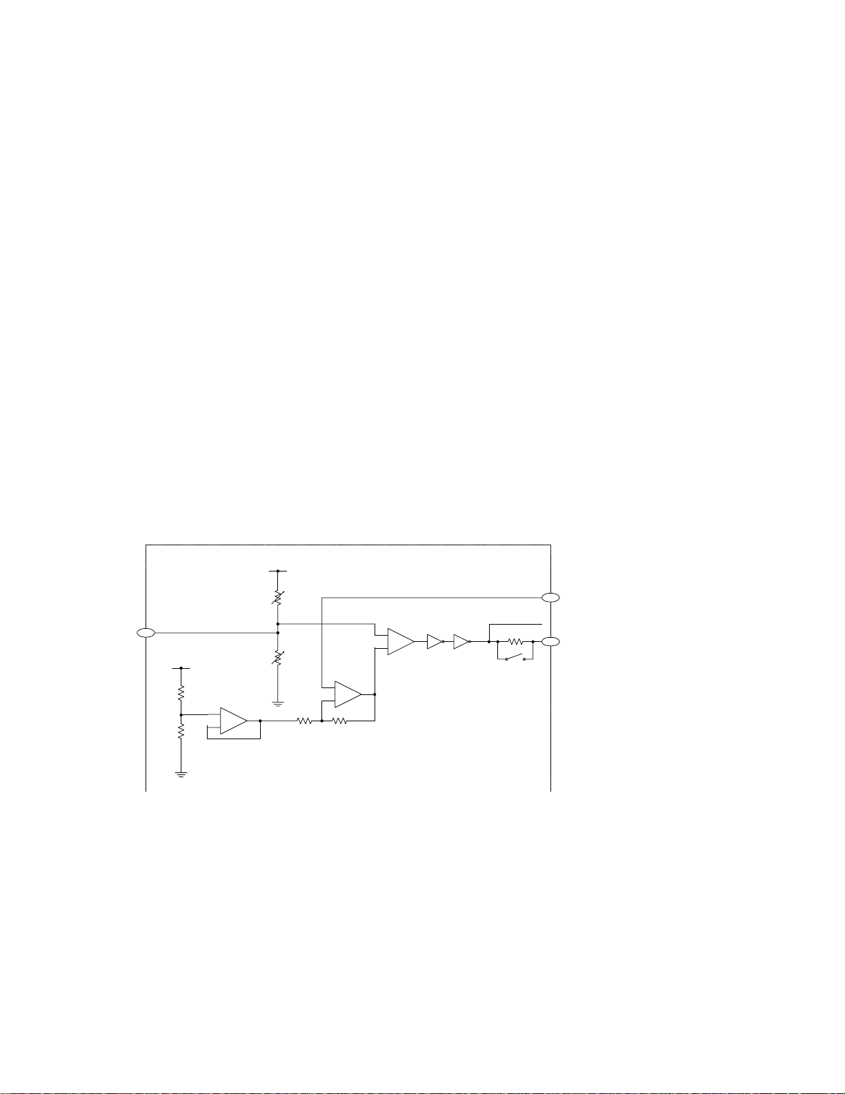
The tracking zero-cross signal (hereinafter TEC signal) is obtained by amplifying the TE signal 4 times, and used to
detect the tracking-error zero-cross point.
By using the information on this point, the following two operations can be performed:
1. Track counting in the carriage move and track jump modes
2. Sensing the lens-moving direction at the moment of the tracking close (The sensing result is used for the tracking
brake circuit as explained below.)
The frequency range of the TEC signal is between 300Hz and 20kHz.
TEC voltage = TE level x 4
The TEC level can be calculated at 5.2V. This level exceeds the D range of the operation amplifier, and the signal gets
clipped. However, it can be ignored because the CD LSI only uses the signal at the zero-cross point.
1.1.7 EFM
The EFM circuit converts the RF signal into a digital signal expressed in binary digits 0 and 1. The AGCO output from
the pin 116 is A/C-coupled in the peripheral circuit, fed back to the LSI from the pin 115, and sent to the EFM circuit
inside the LSI.
On scratched or dirty discs, part of the RF signal recorded may be missing. On other discs, part of the RF signal
recorded may be asymmetric, which was caused by dispersion in production quality. Such lack of information cannot
be completely eliminated by this AC coupling process. Therefore, by utilizing the fifty-fifty occurrence ratio of binary
digits (0 and 1) in the EFM signal, the EFM comparator reference voltage ASY is controlled, so that the comparator
level always stays around the center of the RFO signal. The reference voltage ASY is made from the EFM comparator
output via the low-pass filter. The EFM signal is put out from the pin 111.
Fig. 1.1.4 EFM
RFI
115
40K
40K
Vdd
Vdd
112
111
ASY
EFM
UPD63760GJ
EFM
SIGNAL
+
-
+
-
+
1R5K 7R5K
2K
Page 7
7
C X-3007
1.2 SERVO BLOCK (UPD63760GJ: IC201)
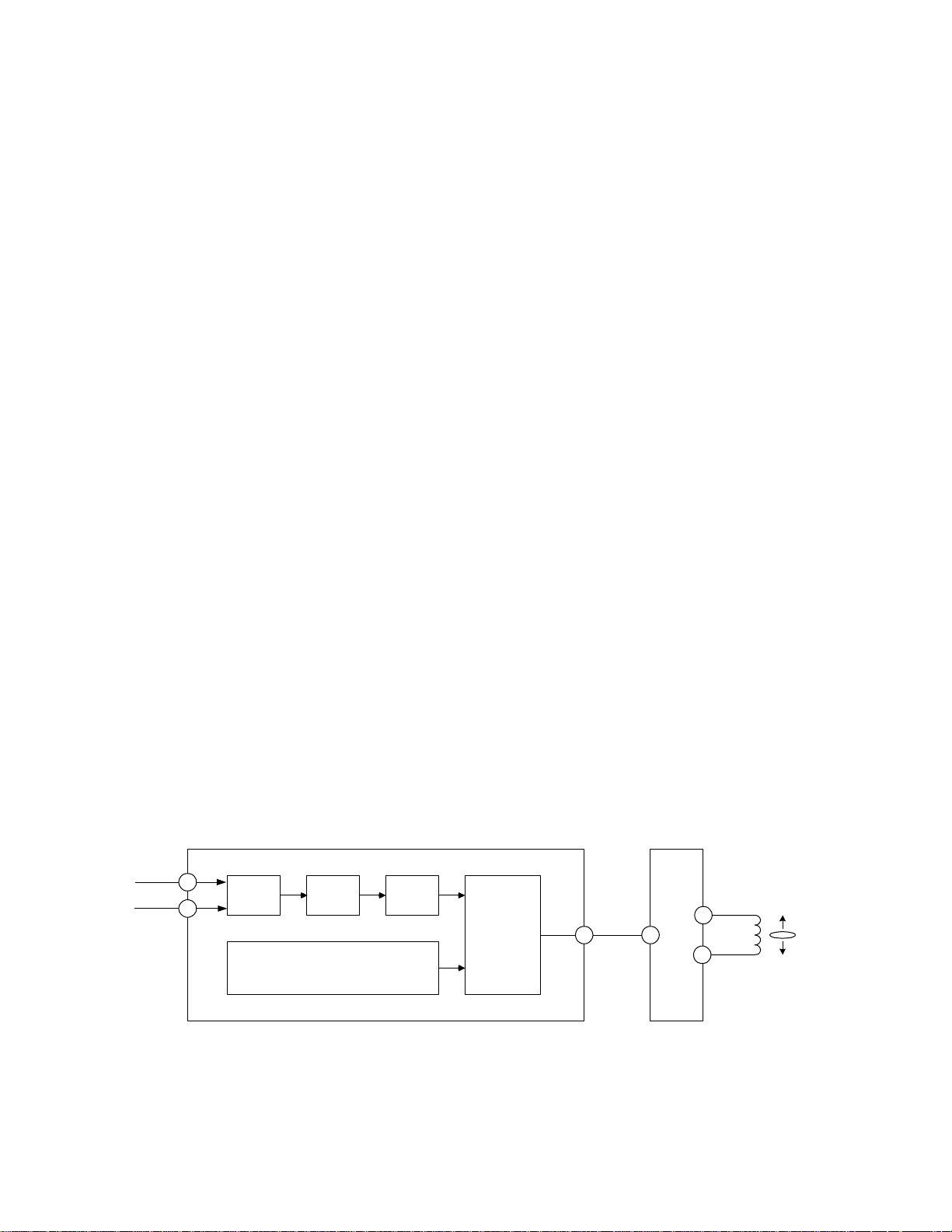
The servo block controls the servo systems for error signal equalizing, in-focus, track jump and carriage move and so
on. The DSP block is a signal-processing block, where data decoding, error correction, and compensation are
performed.
After A/D-converted, the FE and TE signals (generated in the preamplifier block) are applied to the servo block and
used to generate the drive signals for the focus, tracking, and carriage servos.
The EFM signal is decoded in the DSP block, and finally sent out as the audio signal after D/A-converted. In this
decoding process, the spindle servo error signal is generated, supplied to the spindle servo block, and used to
generate the spindle drive signal.
The drive signals for focus, tracking, carriage, and spindle servos (FD, TD, SD, and MD) are provided as PWM3 data,
and then converted to the analog data by the low-pass filter in the driver IC BA5996FM (IC301). These analog drive
signals can be monitored by the FIN, TIN, CIN, and SIN signals respectively. Afterwards, the signals are amplified and
applied to each servo's actuator and motor.
1.2.1 Focus servo system
In the focus servo system, the digital equalizer block works as its main equalizer. The figure 1.2.1 shows the block
diagram of the focus servo system.
To close the focus loop circuit, the lens should be moved to within the in-focus range. While moving the lens up and
down by using the focus search triangular signal, the system tries to find the in-focus point. In the meantime, the
spindle motor rotation is kept at the prescribed one by using the kick mode.
The servo LSI monitors the FE and RFOK signals and automatically performs the focus close operations at an
appropriate timing. The focus loop will close when the following three conditions are satisfied at the same time:
1) The lens moves toward the disc surface.
2) The RFOK signal is shifted to "H".
3) The FE signal is zero-crossed. At last, the FE signal comes to the zero level (or REFO).
When the focus loop is closed, the FSS bit is shifted from "H" to "L". The microcomputer starts monitoring the RFOK
signal obtained through the low-pass filter 10msec after that.
If the RFOK signal is detected as "L", the microcomputer will take several actions including protection.
The timing chart for focus close operations is shown in fig. 1.2.2. (This shows the case where the system fails focus
close.)
In the test mode, the S-shaped curve, search voltage, and actual lens movement can be confirmed by pressing the
focus close button when the focus mode selector displays 01.
Fig. 1.2.1 Block diagram of the focus servo system
IC201 UPD63760GJ
A+C
B+D
124
127
FE
AMP
WAVE GENERATOR
A/D
FOCUS SEARCH
TRIANGULAR
DIG.
EQ
CONTROL
105
PWM
IC301 BA5996FM
FD
6
12
11
FOP
LENS
FOM
Page 8

8
C X-3007
Fig. 1.2.2 Timing chart for focus close operations
1.2.2 Tracking servo system
In the tracking servo system, the digital equalizer block is used as its main equalizer. The figure 1.2.3 shows the block
diagram of the focus servo system.
(a) Track jump
Track jump operation is automatically performed by the auto-sequence function inside the LSI with a command from
the microcomputer. In the search mode, the following five track jump modes are available: 1, 4, 10, 32, and 32*3
In the test mode, 1, 32, and 32*3 track jump modes, and carriage move mode are available and can be switched by
selecting the mode.
For track jumps, first, the microcomputer sets about half the number of tracks to be jumped as the target. (Ex. For 10
track jumps, it should be 5 or so.) Using the TEC signal, the microcomputer counts up tracks. When the counter
reaches the target set by the microcomputer, a brake pulse is sent out to stop the lens. The pulse width is determined
by the microcomputer. Then, the system closes the tracking loop and proceeds to the normal play. At this moment, to
make it easier to close the tracking loop, the brake circuit is kept ON for 50msec after the brake pulse, and the tracking
servo gain is increased.
In the normal operation mode, the FF/REW operation is realized by continuously repeating single jumps about 10
times faster than the normal single jump operation.
(b) Brake circuit
The brake circuit stabilizes the servo-loop close operation even under poor conditions, especially in the setting-up
mode or track jump mode. This circuit detects the lens-moving direction and emits only the drive signal for the
opposite direction to slow down the lens. Thus, this makes it easier to close the tracking servo loop. The off-track
direction is detected from the phases of the TEC and MIRR signals.
Output from FD terminal
Search start
A blind period
FE controlling signals
FSS bit of SRVSTS1 resistor
RFOK signals
The broken line in the figure is assumed in the case
without focus servo.
You can ignore this for blind periods.
The status of focus close is judged from the statuses
of FSS and RFOK after about 10mS.
Page 9

9
C X-3007
Fig. 1.2.3 Block diagram of the tracking servo system
Fig. 1.2.4 Single-track jump
IC201 UPD63760GJ
129
E
128
F
TE
AMP
A/D
DIG.
EQ
JUMP
PARAMETERS
BRAKE
TD
t2
t1
KICK
CONTROL
106
PWM
TD
IC301 BA5996FM
13
14
TOP
TOM
LENS
3
TEC
T. BRAKE
EQUALIZER
T. SERVO
GAIN NORMAL
ON
OFF
GAIN UP
NORMAL
OPEN
CLOSED
Page 10

10
C X-3007
Fig. 1.2.5 Multi-track jump
Fig. 1.2.6 Track brake
TD
TEC
(10 TRACK)
EQUALIZER
T. BRAKE
SERVO
SD
t1
t2
50mS
t
2.9mS (4.10 TRACK JUMP)
5.8mS (32 TRACK JUMP)
GAIN UP
NORMAL
ON
OFF
OPEN
CLOSED
TEC
TZC
(TEC "SQUARED UP" )
(INTERNAL SIGNAL )
MIRR
MIRR LATCHED AT
TZC EDGES
=
SWITCHING PULSE
EQUALIZER OUTPUT
(SWITCHED)
DRIVE DIRECTION
LENS MOVING FORWARDS
(INNER TRACK TO OUTER)
REVERSE
LENS MOVING BACKWARDS
FORWARD
Time
Note : Equalizer output assumed to hava same phase as TEC.
Page 11

11
C X-3007
1.2.3 Carriage servo system
In the carriage servo system, the low frequency component from the tracking equalizer (the information on the lens
position) is transferred to the carriage equalizer, where the gain is increased to a certain level, and then sent out from
the LSI as the carriage drive signal. This signal is applied to the carriage motor via the driver IC.
During the play mode, when the lens offset reaches a certain level, it is necessary to move the pickup toward the
FORWARD direction. The equalizer gain is adjusted so that the output over the carriage motor starting voltage is sent
out in such a case. In actual operations, only when the equalizer output exceeds the threshold level preset in the servo
LSI, the drive signal is sent out. This can reduce the consumption power.
With an eccentric disc loaded, before the whole pickup starts moving, the equalizer output may exceed the threshold
level a few times. In this case, the drive signal applied from the LSI shows pulse-like waveforms.
Fig. 1.2.7 Block diagram for the carriage servo block
Fig. 1.2.8 Waveforms of the carriage signal
IC201 UPD63760GJ
From
TRACK EQ.
DIG.
EQ
CONTROL
KICK, BRAKE
REGISTERS
TRACKING DRIVE
(LOW FREQUENCY)
LENS POSITION
107 24
PWM
SD
IC301 BA5996FM
18
LCOP
17
LCOM
M
CARRIAGE
MOTOR
CRG DRIVE
(INSIDE UPD63711GC)
CRG MOTOR VOLTAGE
DRIVE ON/OFF THRESHOLD
CARRIAGE MOVED AT THESE POINTS
Page 12

12
C X-3007
1.2.4 Spindle servo system
In the spindle servo system, the following six modes are available:
1) Kick
Used to accelerate the disc rotation in the setting-up mode.
2) Offset
a. Used in the setting-up mode until the AGC completes after the kick mode.
b. Used when the focus loop is unlocked during the play mode and until it is locked again.
In both cases, the mode is to keep the disc rotation near to the appropriate one.
3) Applicable servo
In the normal operation, the CLV servo mode is used.
The EFM demodulation block detects through WFCK/16 sampling whether or not the frame sync signal and the
internal frame counter output are synchronized, and generates the status signal based on the sampling result,
synchronized or non-synchronized. If eight consecutive "non-sync" signals are obtained, the system senses the status
as "non-sync". If not, the system senses as "sync". In the applicable servo mode, the leading-in servo mode is
automatically selected at the non-sync status, and the normal servo mode is at the sync status.
4) Brake
Used to stop the spindle motor.
In accordance with the microcomputer's command, the brake voltage is sent out from the servo LSI. At this moment,
the EFM waveform is being monitored in this LSI. When the longest EFM pattern exceeds a certain cycle (or the
rotation slows down enough), a flag is set inside the LSI, and the microcomputer switches off the brake voltage. If a
flag is not set within a certain period, the microcomputer shifts the mode from the brake mode to the stop mode, and
keeps this for a certain period. In the eject mode, after the mode is shifted to the stop mode and a certain period
passes, the loaded disc is ejected.
5) Stop
Used when the power is turned on and during the eject mode. At this moment, the voltage through the spindle motor
is 0V.
6) Rough servo
Used when the carriage is moved (or in the carriage move mode such as long search).
By obtaining the linear velocity from the EFM waveform, "H" or "L" is applied to the spindle equalizer. In the test
mode, this mode is used for grating confirmation.
Fig.1.2.9 Block diagram of the spindle servo system
IC201 UPD63760GJ
SPEED ERROR SIGNAL
EFM
SIGNAL
DSP
BLOCK
PHASE ERROR SIGNAL
DIG.
EQ
PWM
108
IC301 BA5996FM
MD
26
16
15
SOP
M
SOM
SPINDLE
MOTOR
Page 13

13
C X-3007
1.3 AUTOMATIC ADJUSTMENT FUNCTION
This system automatically handles the circuit adjustment inside the CD LSI. All adjustments are performed whenever
a disc is inserted or the CD mode is selected by pressing the source key. Each adjustment will be explained below.
1.3.1 TE, FE, and RF offset auto-adjustment
This adjustment is made to adjust the offsets of the TE, FE, and RF amplifiers in the preamplifier block to their target
values on the basis of the REFO when the power is turned on. (The target values for TE, FE, and RE offsets are 0V, 0V,
and -0.8V respectively.)
<Adjusting procedures>
1) With the LD OFF status, the microcomputer reads each offset through the servo LSI.
2) The microcomputer calculates the voltages for correction from the measured values, and inputs the calculated
results as the offset adjustment values.
1.3.2 Tracking balance (T.BAL) auto-adjustment
This adjustment is to equalize the pickup output offsets for E-ch and F-ch by changing the amplifier gain inside the LSI.
Actually, the gain is adjusted so that the TE waveform becomes symmetrical on each side of the REFO.
<Adjusting procedures>
1) The focus loop is closed.
2) The lens is kicked in the radial direction to make certain that the TE waveform is generated.
3) The microcomputer reads the TE offset calculated in the LSI through the servo LSI.
4) The microcomputer takes either of the following steps depending on the calculated offset:
• When the offset is 0, the adjustment completes.
• When the offset is positive or negative, the amp gains for E-ch and F-ch should be changed.
The steps 2) to 4) are repeatedly taken until the offset becomes 0 or the repeating time reaches the limit frequency.
1.3.3 EF bias auto-adjustment
This adjustment obtains the best focus point during the play mode and maximizes the RFI level by utilizing the phase
difference between the 3T level of the RF signal and that of the signal obtained when focus error disturbance is applied
to the focus loop. At this moment, the auto-gain control (AGC), where focus error disturbance is applied to the focus
and tracking loops, is also performed as explained below.
<Adjusting procedures>
1) The microcomputer transmits the command to apply disturbance component to the focus loop (inside the servo
LSI).
2) In the LSI, the 3T-offset component of the RF signal is detected.
3) From the relation between the 3T detected component and the disturbance, the LSI obtains the volume and
direction of the focus offset.
4) The microcomputer transmits the command and reads out the detecting result from the servo LSI.
5) The microcomputer calculates the necessary correction and inputs the result as the bias adjustment value to the
servo LSI.
The adjusting steps are repeated a few times for higher adjustment accuracy as same as those for the AGC.
1.3.4 Focus and tracking AGC
This function automatically adjusts the focus and tracking servo loop gains.
<Adjusting procedures>
1) Disturbance component is applied to the servo loop.
2) The error signals (FE and TE) are extracted through the band pass filter as the G1 and G2 signals.
3) The microcomputer reads the G1 and G2 signals through the servo LSI.
4) The microcomputer calculates the necessary correction and performs the loop gain adjustment inside the servo LSI.
For higher adjustment accuracy, the above steps are repeated a few times.
Page 14

14
C X-3007
1.3.5 RF level auto-adjustment (RFAGC)
This adjustment minimizes the dispersion of the RF level (RFO), which may be caused by disc-related errors, for more
stable signal transmission by changing the amp gain between RFI and RFO.
<Adjusting procedures>
1) The microcomputer sends the command to the servo LSI to read out the output from the RF level detecting circuit
inside the servo LSI.
2) The microcomputer calculates the appropriate amp gain by using the output read out to adjust the RFO level at the
prescribed one.
3) The microcomputer sends the command to the servo LSI to adjust the amp gain into the calculated one.
This adjustment is automatically performed when:
1) During the setting-up mode, only the focus close operation ends.
2) Immediately before the setting-up ends (or right before the play mode starts)
3) During the play mode, the focus loop is locked again after unlocked.
1.3.6 Pre-amp gain adjustment
In this adjustment, when the reflected beams from disc surface are extremely weak (ex. when the lens is dirty, and a
CD-RW is loaded), the whole gain in the RFAMP block (FE, TE, and RF amplifiers) is increased by +6dB or +12dB.
<Adjusting procedures>
When the system senses that the reflected beams from disc surface are extremely weak during the setting-up mode,
the whole RFAMP gain is increased by +6dB or +12dB.
After the gain is changed, the setting-up mode is restarted.
If the whole RFAMP gain is always increased to the +6dB level in the play mode, the +6dB level will be employed at the
starting of the setting-up mode from the next playback.
Fig.1.3.1 Pre-amp gain adjustment
Gain of entire RFAMP
+ 12dB
+ 6dB
TYP
Play at +6dB increases due to stained lens or other reasons
(the typical gain is employed for the initial setup)
Play the CD-RW with the gain being set to +12dB
Play is started with +6dB
judging the lens is stained
Time
Page 15

15
C X-3007
1.3.7 Initial values in adjustment
For each auto-adjustment, the last adjustment results are basically used as the initial settings of the next adjustment
unless the microcomputer is turned off (or the backup is off). When the microcomputer (or the backup) is turned off,
the last adjustment results are not used, but the factory settings.
1.3.8 Adjustment result display
For some of the adjustments (FE and RF offset, FZD cancel, F and T gain, and RFAGC), the adjustment results can be
displayed and confirmed in the test mode.
1) FE and RF offset
Reference coefficient = 32 ("32" indicates no adjustment required)
The display is expressed in the unit of about 32mV.
Ex. When the FE offset coefficient is 35:
35 - 32 = 3 x 32mV = 96mV
This means that the correction is about +96mV, and the FE offset before adjustment is -96mV.
2) F and T gain adjustment
Reference coefficient for focus and tracking = 20
The displayed coefficient / the reference coefficient indicates the adjusted gain.
Ex. When the AGC coefficient is 40:
40/20 = 2 times (+6dB)
That is, the gain was adjusted by +6dB.
(The original loop gain was half the target one. So, the whole gain was doubled.)
3) RF level adjustment (RFAGC)
Reference coefficient = 8
The coefficient 9 to 15 indicates increasing the RF level.
The coefficient 0 to 7 indicates decreasing the RF level.
When the coefficient display changes by 1, the gain changes by 0.7 to 1dB.
When the coefficient is 15, the gain is maximum or TYP + 6.5dB.
When the coefficient is 0, the gain is minimum or TYP - 6.0dB.
Page 16

16
C X-3007
1.4 POWER SUPPLY AND LOADING BLOCK
The VD (8.3 + 0.5V) and the VDD (5.0 + 0.25V), which are supplied from the mother PC board, are used for the power
supply. In this system, the following four power-supply signals are available: the VD (for the drive system), the V3R3
obtained from the VD via the 3.3V regulator (for the control system: 3.3V), the VDD (for the microcomputer: 5V), and
the 3VDD obtained from the VDD via the 3.3V regulator (for the microcomputer: 3.3V)
In the WMA-supported mechanism CXK5556, the V2R5 (for WMA decoder: 2.5V) is also used.
The microcomputer can turn on/off the CD driver (except for the load and eject modes) and the 5V signal by
controlling the "CONT" and "CD5VON" signals respectively. To turn on/off the loading drive, there is no control
terminal in the microcomputer, but the "LOEJ" input signal works as the control one. In the LCO output block, the
"CLCONT" signal is used to switch between the loading mode and carriage mode.
Fig. 1.4.1 Power supply/loading block (*: CXK5556, CXK5557)
Fig. 1.4.2 Loading/carriage mode shift
CN901
470/10
+
18
PGND
19
VD
2
3
VDOUT
9
16
17
VDCONT
13
1
20
IC301
10
19
28
BA5996FM
BA033SFP
GND
VDD
LCOP
18
LOADING
M
LCOM
17
9
22
21
IC203
3 3
IC703
2
MOTOR
1 122
V3R3D
4 4
BA25BC0WFP
4
5
1
*IC502
3VDD
CD3VON
CLCONT
28
V2R5
5VDD
CONT
LOEJ
2932 31
IC701
PE5268
*PE5269
27 78
DSCSNS
S902 S904 S905 S903
S-818AA33AUC-BGN
CLCLONT
Loading Mode Loading Mode
Carriage Mode
Page 17

17
C X-3007
To control the load and eject operations, the clamp switch located in the mechanism unit and the three detecting
switches located in the control unit are used. Depending on the combination of these switches' ON/OFF status, the
DSCSNS voltage changes.
The microcomputer can detect the status (A to E) by observing the voltage at the A/D port. The disc size detection (8
or 12cm) is also performed through this status change. The DSCSNS status and the status change in the load and
eject modes are shown in the figures 1.4.3 and 1.4.4 respectively.
Fig.1.4.3 DSCSNS status
Fig.1.4.4 Status change in LOAD and EJECT modes
STATUS A B C D E
SW1(S903) ON OFF OFF OFF ON
SW2(S905) OFF OFF ON ON OFF
SW3(S904) OFF OFF OFF ON OFF
SW4(S902) OFF OFF OFF OFF ON
MECH. STATUS NO DISK CLAMP
LOADING
12cm
B
A
C
D
E
A/D A B C D C B E
CLCONT
LOEJ
MOTOR
STOP LOAD STOP
8cm
B
A
C
D
E
A/D A B C B A or B B E
CLCONT
LOEJ
MOTOR
STOP LOAD STOP
EJECT
12cm
B
A
D
E
A/D E B C D C
CLCONT
LOEJ
MOTOR
STOP EJECT STOP
CARRIAGE/LOAD SWITCHING
8cm
B
A
C
D
E
A/D E B A or B B C
CLCONT
LOEJ
MOTOR
STOP EJECT STOP
CARRIAGE/LOAD SWITCHING
12cm RECOGNITION CHECK
DEAD ZONE
LOAD/CARRIAGE SWITCHING
DEAD ZONE
LOAD/CARRIAGE SWITCHING
8cm RECOGNITION CHECK
B
Page 18

18
C X-3007
- Loading actions
1. When a disk is inserted, SW Arm L and R rotate. Due to the rotation of Arm L, SW1 is switched from ON to OFF and
the Load Carriage Motor starts.
2. If the disk is 12cm-disk, when it is carried to the position shown with the dotted line in the drawing, SW 3 switches
to ON due to such rotation of Arm L. Then, the microcomputer judges that the disk is 12cm-disk.
3. In case of 8cm-disk, the disk cannot reach such dotted line position, and from such limitation of approach, the
microcomputer judges that the disk is 8cm-disk and simply triggers clamp actions.
(Movement of SW Arm L and R are connected together. So, if pushing force is fed to only one arm, the distance
between tow arms cannot be widened beyond the specific degree, because the coupling part is locked in such case.)
- Disk centering mechanism
1. In case of 12cm-disk, the 12cm-Disk Detection Arm rotates, and with such rotation, it raises the Centering Arms to
retreat the arms from disk's trace. The disk passes through under the arms, and at the inner part, it is centered.
2. In case of 8cm-disk, it is just centered at the position where its edge touches the front portion of the Centering Arm.
2. MECHANISM DESCRIPTIONS
Page 19

19
C X-3007
- Clamp actions
1. When centering of 12 or 8cm-disk onto the Spindle is completed, the Detection Arm starts driving.
2. Then, the Detection Arm, via the Detection Reversion Arm, triggers driving of the Plunging Rack, which is on the
Mode Switching Arm unit, in order to engage the rack with the 2-Stage Gear.
3. With such engaging, the Mode Switching Arm rotates, and with the rotation, slides the Clamp-Up Lever and pushes
down the Clamp Arm. At the same time, the Mode Switching Arm slides the Loading-Up lever, and separates the
Loading Arm from the disk. Also, the Loading-Up Lever rotates the Mechanics Lock Arm, releases the Mechanics
Lock, and switches on the Clamp SW. Now, at this position (the position where the disk is situated when the Clamp
SW is switched on), clamping actions are completed.
4. Then, upon the completion of clamping actions, the Plunging Rack lets the Pickup Lock Arm start rotating, and this
Pickup Lock Arm, with such rotation, feeds the Pickup to Feed Screw's screw portion. Now, Carriage actions start.
- Eject actions
1. Eject actions start when the Pickup is fed to the position inner than "Home SW ON" point in the internal
circumference of the circle, caused by backward rotation of the Load Carriage Motor. Eject actions follow the
foregoing procedures (steps taken in loading, centering and clamping actions), but each action in those steps is
performed in reversed manner.
2. In case of 12cm-disk, Eject is completed when SW3 completes its condition- transition of OFF → ON → OFF.
3. For 8cm-disk, Eject is completed when SW2 completes its condition-transition of OFF → ON → OFF.
Page 20

20
C X-3007
- How to hold the Mechanical Unit
1.Hold the top and bottom frame.
2.Do not squeeze top frame's front portion too tight,
because it is fragile.
- How to remove the Top and Bottom Frame
1.When the disk is in "clamp" state, unlock Spring A (6
pieces) and Spring B (2 pieces), and unscrew screws
(4 pieces).
2.Unlock each 1 of pawl at the both side of the frame,
then remove the top frame.
3.Remove the Carriage Mechanical part in such way
that; you remove the mechanical part from 3 pieces
of Damper while slowly pulling up the part.
4.Now, the top frame has been removed, and under
this state, fix the genuine Connector again, and eject
the disk.
(Caution)
When you reassemble the Carriage Mechanical part,
apply a bit of alcohol to Dampers.
- How to remove the Guide Arm Assy
1.Unlock the spring (1 piece) at the right side of the
assembly.
2.Unscrew screws (2 pieces), then remove the Screw
Gear Bracket.
3.Shift the Guide Arm Assy to the left and slowly rotate
it to the upper direction.
4.When the Guide Arm Assy rotates approximately 45
degree, shift the Assy to the right side direction and
remove it.
Top Frame
Bottom Frame
Damper
Spring
Screw Gear Bracket
Guide Arm
Assy
Carriage
Mechanical
Part
Do not squeeze.
3. DISASSEMBLY
Page 21

21
C X-3007
- How to remove the Control Unit
1.Give jumper-solder treatment to the Flexible Wire of
the Pickup unit, then remove the wire from the
Connector.
2.Remove all 4 points of solder-treatment on the Lead
Wire. Also, unscrew the screw(1 piece).
3.Then, Remove the Control unit.
(Caution)
Be careful not to damage SW when you reassemble
the Control Unit into the device.
- How to remove the Loading Arm Assy
1.Unlock the spring (1 piece) and remove the E ring (1
piece) of the Fulcrum Shaft.
2.Shift the arm to the left side direction and unlock pins
(2 pieces).
- How to remove the Pickup Unit
1.Unscrew 2 pieces of screws, then remove the Pulley
Cover.
2.Remove the Feed Screw unit from the pawl of the
Feed Screw Guide (The pawl is located inside the
guide).
3.Remove the belt from the Pulley, then remove the
Pickup unit.
(Caution)
Make sure not to stain the belt with grease when you
fix the belt.
Control Unit
Jumper-Solder
Solder
Loading Arm Assy
Pickup Unit
Pulley Cover
Feed Screw Guide
Belt
Grease Application
Grease Application
Grease Application
Page 22

C X-3007
- How to remove the Load Carriage Motor Assy
1.Unscrew the screw (1 piece).
2.Remove the Load Carriage Motor Assy.
- How to remove the Clamp Arm Assy
1.Unlock springs (3 pieces).
2.Remove the Clamp-Up Lever.
3.Remove the Assy in such way that; you shift the Assy
to the left side direction while you rotate it to the
upper direction slowly.
- How to remove the Spindle Motor
1.Unscrew 2 pieces of screws. Then you can remove
the motor.
Load Carriage
Motor Assy
Clamp-Up Lever
Spindle Motor
Clamp Arm Assy
Spring
Spring
Spring
Grease Application
 Loading...