

Page 1
PIONEER CORPORATION 4-1, Meguro 1-chome, Meguro-ku, Tokyo 153-8654, Japan
PIONEER ELECTRONICS (USA) INC. P.O. Box 1760, Long Beach, CA 90801-1760, U.S.A.
PIONEER EUROPE NV Haven 1087, Keetberglaan 1, 9120 Melsele, Belgium
PIONEER ELECTRONICS ASIACENTRE PTE. LTD. 253 Alexandra Road, #04-01, Singapore 159936
PIONEER CORPORATION 2006
FL DIMMER
HD HDMI LAN FL OFF
STANDBY/ON
ORDER NO.
RRV3466
BDP-HD1
Blu-ray Disc PLAYER
BDP-HD1
THIS MANUAL IS APPLICABLE TO THE FOLLOWING MODEL(S) AND TYPE(S).
Model Type Power Requirement Region No. Remarks
BDP-HD1 KU/CA AC120 V 1
BD Region A
For details, refer to "Important symbols for good services".
T-ZZR DEC. 2006 printed in Japan
Page 2
-
1234
SAFETY INFORMATION
A
This service manual is intended for qualified service technicians ; it is not meant for the casual do-it
yourselfer. Qualified technicians have the necessary test equipment and tools, and have been trained
to properly and safely repair complex products such as those covered by this manual.
Improperly performed repairs can adversely affect the safety and reliability of the product and may
void the warranty. If you are not qualified to perform the repair of this product properly and safely, you
should not risk trying to do so and refer the repair to a qualified service technician.
WARNING
This product contains lead in solder and certain electrical parts contain chemicals which are known to the state of California to
causecancer, birth defects or other reproductive harm.
B
NOTICE
(FOR CANADIAN MODEL ONLY)
Fuse symbols (fast operating fuse) and/or (slow operating fuse) on PCB indicate that replacement
parts must be of identical designation.
REMARQUE
(POUR MODÈLE CANADIEN SEULEMENT)
Les symboles de fusible (fusible de type rapide) et/ou (fusible de type lent) sur CCI indiquent que
les pièces de remplacement doivent avoir la même désignation.
C
(FOR USA MODEL ONLY)
Health & Safety Code Section 25249.6 – Proposition 65
1. SAFETY PRECAUTIONS
The following check should be performed for the
continued protection of the customer and
service technician.
ANY MEASUREMENTS NOT WITHIN THE LIMITS
OUTLINED ABOVE ARE INDICATIVE OF A POTENTIAL
SHOCK HAZARD AND MUST BE CORRECTED BEFORE
RETURNING THE APPLIANCE TO THE CUSTOMER.
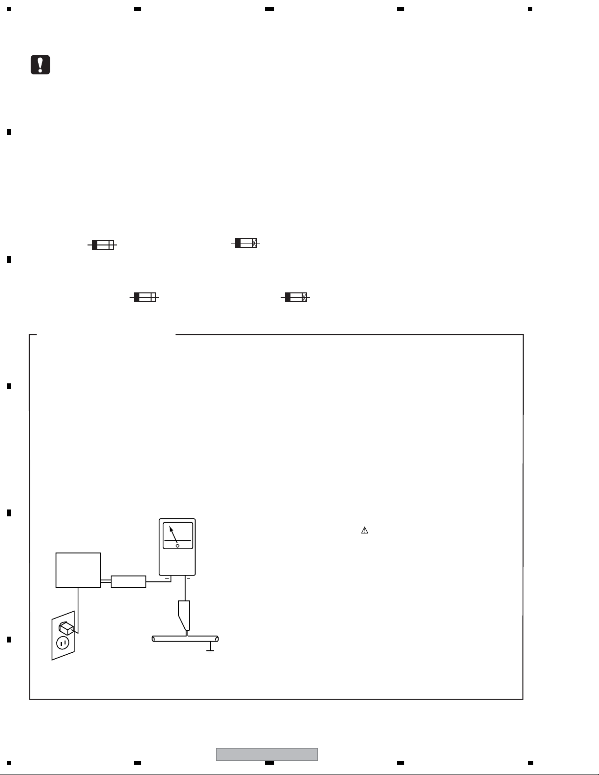
LEAKAGE CURRENT CHECK
Measure leakage current to a known earth ground (waterpipe
, conduit, etc.) by connecting a leakage current tester
D
E
such as Simpson Model 229-2 or equivalent between the
earth ground and all exposed metal parts of the appliance
(input/output terminals, screwheads, metal overlays, control
shaft, etc.). Plug the AC line cord of the appliance directly
into a 120V AC 60Hz outlet and turn the AC power switch
on. Any current measured must not exceed 0.5mA.
Reading should
not be above
0.5mA
Earth
ground
Device
under
test
Also test with
plug reversed
(Using AC adapter
plug as required)
Test all
exposed metal
surfaces
Leakage
current
tester
2. PRODUCT SAFETY NOTICE
Many electrical and mechanical parts in the appliance
have special safety related characteristics. These are
often not evident from visual inspection nor the protection
afforded by them necessarily can be obtained by using
replacement components rated for voltage, wattage, etc.
Replacement parts which have these special safety
characteristics are identified in this Service Manual.
Electrical components having such features are identified
by marking with a on the schematics and on the parts list
in this Service Manual.
The use of a substitute replacement component which does
not have the same safety characteristics as the PIONEER
recommended replacement one, shown in the parts list in
this Service Manual, may create shock, fire, or other hazards.
Product Safety is continuously under review and new
instructions are issued from time to time. For the latest
information, always consult the current PIONEER Service
Manual. A subscription to, or additional copies of, PIONEER
Service Manual may be obtained at a nominal charge
from PIONEER.
AC Leakage Test
F
2
1234
BDP-HD1
Page 3
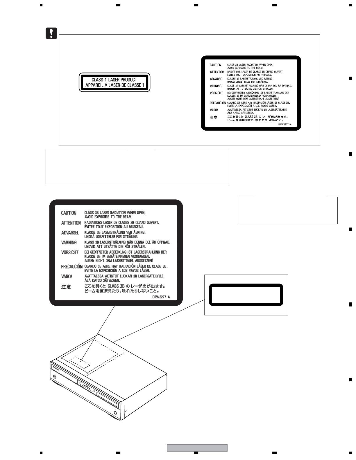
5 678
CAUTION
This product is a class 1 laser product, but this
product contains a laser diode higher than Class 1.
The following caution label appears on your unit.
Location: inside of the unit
To ensure continued safety, do not remove any covers
or attempt to gain access to the inside of the product.
Refer all servicing to qualified personnel.
WARNING !
THE AEL (ACCESSIBLE EMISSION LEVEL) OF THE LASER POWER OUTPUT IS LESS THAN
CLASS 1 BUT THE LASER COMPONENT IS CAPABLE OF EMITTING RADIATION
EXCEEDING THE LIMIT FOR CLASS 1.
A SPECIALLY INSTRUCTED PERSON SHOULD DO SERVICING OPERATION OF THE
APPARATUS.
LABEL CHECK
A
B
C
LASER DIODE CHARACTERISTICS
FOR DVD : MAXIMUM OUTPUT POWER : 5 mW
WAVELENGTH : 650 nm
FOR CD : MAXIMUM OUTPUT POWER : 7 mW
WAVELENGTH : 780 nm
(Printed on the Rear Panel)
D
CLASS 1 LASER PRODUCT
APPAREIL A LASER DE CLASSE 1
E
S
T
A
N
D
B
Y
/O
N
HD
HDM
I
LAN
F
L
D
I
M
M
E
R
FL OFF
F
56
BDP-HD1
7
8
3
Page 4
1234
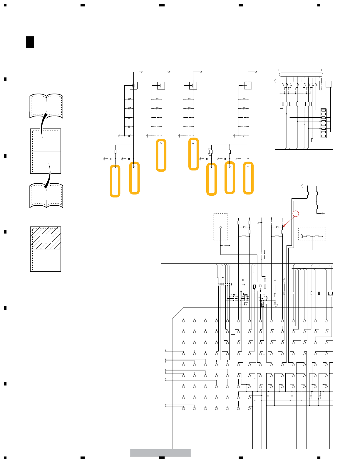
[Important Check Points for Good Servicing]
In this manual, procedures that must be performed during repairs are marked with the below symbol.
A
Please be sure to confirm and follow these procedures.
1. Product safety
Please conform to product regulations (such as safety and radiation regulations), and maintain a safe servicing environment by
following the safety instructions described in this manual.
1 Use specified parts for repair.
Use genuine parts. Be sure to use important parts for safety.
2 Do not perform modifications without proper instructions.
Please follow the specified safety methods when modification(addition/change of parts) is required due to interferences such as
B
C
D
radio/TV interference and foreign noise.
3 Make sure the soldering of repaired locations is properly performed.
When you solder while repairing, please be sure that there are no cold solder and other debris.
Soldering should be finished with the proper quantity. (Refer to the example)
4 Make sure the screws are tightly fastened.
Please be sure that all screws are fastened, and that there are no loose screws.
5 Make sure each connectors are correctly inserted.
Please be sure that all connectors are inserted, and that there are no imperfect insertion.
6 Make sure the wiring cables are set to their original state.
Please replace the wiring and cables to the original state after repairs.
In addition, be sure that there are no pinched wires, etc.
7 Make sure screws and soldering scraps do not remain inside the product.
Please check that neither solder debris nor screws remain inside the product.
8 There should be no semi-broken wires, scratches, melting, etc. on the coating of the power cord.
Damaged power cords may lead to fire accidents, so please be sure that there are no damages.
If you find a damaged power cord, please exchange it with a suitable one.
9 There should be no spark traces or similar marks on the power plug.
When spark traces or similar marks are found on the power supply plug, please check the connection and advise on secure
connections and suitable usage. Please exchange the power cord if necessary.
0 Safe environment should be secured during servicing.
When you perform repairs, please pay attention to static electricity, furniture, household articles, etc. in order to prevent injuries.
Please pay attention to your surroundings and repair safely.
2. Adjustments
To keep the original performance of the products, optimum adjustments and confirmation of characteristics within specification.
Adjustments should be performed in accordance with the procedures/instructions described in this manual.
3. Lubricants, Glues, and Replacement parts
E
Use grease and adhesives that are equal to the specified substance.
Make sure the proper amount is applied.
4. Cleaning
For parts that require cleaning, such as optical pickups, tape deck heads, lenses and mirrors used in projection monitors, proper
cleaning should be performed to restore their performances.
5. Shipping mode and Shipping screws
To protect products from damages or failures during transit, the shipping mode should be set or the shipping screws should be
installed before shipment. Please be sure to follow this method especially if it is specified in this manual.
F
4
1234
BDP-HD1
Page 5

5 678
CONTENTS
SAFETY INFORMATION......................................................................................................................................2
1. SPECIFICATIONS .............................................................................................................................................6
2. EXPLODED VIEWS AND PARTS LIST.............................................................................................................8
2.1 PACKING....................................................................................................................................................8
2.2 EXTERIOR SECTION ..............................................................................................................................10
2.3 FRONT PANEL SECTION ........................................................................................................................12
3. BLOCK DIAGRAM AND SCHEMATIC DIAGRAM ..........................................................................................14
3.1 BLOCK DIAGRAM....................................................................................................................................14
3.2 POWER BLOCK.......................................................................................................................................15
3.3 OVERALL WIRING DIAGRAM .................................................................................................................16
3.4 MAIN ASSY 1/7 ........................................................................................................................................18
3.5 MAIN ASSY 2/7 ........................................................................................................................................22
3.6 MAIN ASSY 3/7 ........................................................................................................................................24
3.7 MAIN ASSY 4/7 ........................................................................................................................................26
3.8 MAIN ASSY 5/7 ........................................................................................................................................28
3.9 MAIN ASSY 6/7 ........................................................................................................................................30
3.10 MAIN ASSY 7/7 ......................................................................................................................................32
3.11 FLKY and PSWB ASSYS .......................................................................................................................34
3.12 AUJB ASSY 1/2......................................................................................................................................36
3.13 AUJB ASSY 2/2......................................................................................................................................38
3.14 SRJB and WRPB ASSYS.......................................................................................................................40
3.15 SYPS ASSY............................................................................................................................................42
3.16 WAVEFORMS.........................................................................................................................................44
4. PCB CONNECTION DIAGRAM ......................................................................................................................46
4.1 AUJB ASSY..............................................................................................................................................46
4.2 MAIN ASSY ..............................................................................................................................................50
4.3 FLKY and PSWB ASSYS .........................................................................................................................54
4.4 SRJB and WRPB ASSYS.........................................................................................................................58
4.5 SYPS ASSY..............................................................................................................................................60
5. PCB PARTS LIST ............................................................................................................................................61
6. ADJUSTMENT ................................................................................................................................................66
6.1 NECESSARY ADJUSTMENT POINTS ....................................................................................................66
6.2 ID NUMBER AND DATA SETTING...........................................................................................................67
6.3 FIRMWARE UPDATE ...............................................................................................................................70
7. GENERAL INFORMATION .............................................................................................................................73
7.1 DIAGNOSIS..............................................................................................................................................73
7.1.1 SERVICE KEY INPUT........................................................................................................................73
7.1.2 SCREEN INDICATION FOR SERVICING..........................................................................................75
7.1.3 HOW TO MEASURE THE ERROR RATE ..........................................................................................76
7.1.4 TROUBLE SHOOTING.......................................................................................................................77
7.2 DISASSEMBLY .........................................................................................................................................79
7.3 PARTS ......................................................................................................................................................82
7.3.1 IC........................................................................................................................................................82
7.4 DISC / CONTENT FORMAT PLAYBACK COMPATIBILITY ....................................................................135
8. PANEL FACILITIES .......................................................................................................................................137
A
B
C
D
56
BDP-HD1
E
F
7
8
5
Page 6

1234
1. SPECIFICATIONS
A
Specifications
Specifications
General
System . . . . . . . . . . . . . . . . . . . . . . . . . . . . . . . . . . . . BD Player
General
System . . . . . . . . . . . . . . . . . . . . . . . . . . . . . . . . . . . . BD Player
Power requirements . . . . . . . . . . . . . . . . . . . . . AC 120 V, 60 Hz
Power consumption . . . . . . . . . . . . . . . . . . . . . . . . . . . . . . 39 W
Power requirements . . . . . . . . . . . . . . . . . . . . . AC 120 V, 60 Hz
Power consumption (standby) . . . . . . . . . . . . . . . . . . . . . . 0.5 W
Power consumption . . . . . . . . . . . . . . . . . . . . . . . . . . . . . . 39 W
B
C
D
Weight . . . . . . . . . . . . . . . . . . . . . . . . . . . . . 6.3 kg (13 lb 15 oz)
Power consumption (standby) . . . . . . . . . . . . . . . . . . . . . . 0.5 W
Dimensions . . . . . . . . . . 420 mm (W) x 94 mm (H) x 359 mm (D)
Weight . . . . . . . . . . . . . . . . . . . . . . . . . . . . . 6.3 kg (13 lb 15 oz)
Dimensions . . . . . . . . . . 420 mm (W) x 94 mm (H) x 359 mm (D)
Operating temperature . . . . . . . . . . . . . . . . . . . . +5 °C to +35 °C
Operating humidity . . . . . . . . . . . . . . . . . . . . . . . . . . . 5 % to 85 %
Operating temperature . . . . . . . . . . . . . . . . . . . . +5 C to +35 C °°
HDMI output
Operating humidity . . . . . . . . . . . . . . . . . . . . . . . . . . . 5 % to 85 %
HDMI output . . . . . . . . . . . . . . . . . . . . . . . . . . . . . . . . . . . . . 19 pin
HDMI output
HDMI output . . . . . . . . . . . . . . . . . . . . . . . . . . . . . . . . . . . . . 19 pin
Component Video output (Y, PB, PR)
Output level . . . . . . . . . . . . . . . . . . . . . . . . . . . Y: 1.0 Vp-p (75 Ω)
Component Video output (Y, PB, PR)
Output level . . . . . . . . . . . . . . . . . . . . . . . . . . . Y: 1.0 Vp-p (75 Ω )
Jacks . . . . . . . . . . . . . . . . . . . . . . . . . . . . . . . . . . . . . . . RCA jacks
S-Video output
Jacks . . . . . . . . . . . . . . . . . . . . . . . . . . . . . . . . . . . . . . . RCA jacks
Y (luminance) - Output level . . . . . . . . . . . . . . . . . 1 Vp-p (75 Ω)
C (color) - Output level . . . . . . . . . . . . . . . . . . 286 mVp-p (75 Ω)
S-Video output
. . . . . . . . . . . . . . . . . . . . . . . . . . . . . . . . . . . . . . . . S-Video jack
Jack
Y (luminance) - Output level . . . . . . . . . . . . . . . . . 1 Vp-p (75 Ω )
C (color) - Output level . . . . . . . . . . . . . . . . . . 286 mVp-p (75
. . . . . . . . . . . . . . . . . . . . . . . . . . . . . . . . . . . . . . . S-Video jack
Jack
Video output
Output level . . . . . . . . . . . . . . . . . . . . . . . . . . . . . . . . .1 Vp-p (75 Ω)
Jack . . . . . . . . . . . . . . . . . . . . . . . . . . . . . . . . . . . . . . . . . . . RCA jack
Video output
Output level . . . . . . . . . . . . . . . . . . . . . . . . . . . . . . . . 1 Vp-p (75 Ω )
Jack . . . . . . . . . . . . . . . . . . . . . . . . . . . . . . . . . . . . . . . . . . . RCA jack
Audio output (1 stereo pair)
Output level. . . . . . . . . . . . . . . . . . . . . . . . . . . . . .During audio output
Audio output (1 stereo pair)
Number of channels
Output level. . . . . . . . . . . . . . . . . . . . . . . . . . . . During audio output
Jacks . . . . . . . . . . . . . . . . . . . . . . . . . . . . . . . . . . . . . . . . . . . RCA jack
Number of channels
Jacks . . . . . . . . . . . . . . . . . . . . . . . . . . . . . . . . . . . . . . . . . . . RCA jack
(BD-ROM, BD-R/RE, DVD-Video, DVD-R/RW,
network file playback)
(BD-ROM, DVD-Video, DVD-R/RW,
network file playback)
9
/
16
(16 in. (W) x 4
9
/
16
(16 in. (W) x 4 in. (H) x 14 in. (D))
5
/
8
in. (H) x 14
5
/
8
3
/
16
in. (D))
3
/
16
(no condensation)
(no condensation)
PB, PR: 0.7 Vp-p (75 Ω)
PB, PR: 0.7 Vp-p (75
200 mVrms (1 kHz, –20 dB)
. . . . . . . . . . . . . . . . . . . . . . . . . . . . . . . . . . . . . 2
200 mVrms (1 kHz, –20 dB)
. . . . . . . . . . . . . . . . . . . . . . . . . . . . . . . . . . . . . 2
Audio output (multi-channel / L, R, C, SW, LS, RS)
Output level . . . . . . . . . . . . . . . . . . . . . . . . . . . D uring audio output
Audio output (multi-channel / L, R, C, SW, LS, RS)
Output level . . . . . . . . . . . . . . . . . . . . . . . . . . . During audio output
Number of channels . . . . . . . . . . . . . . . . . . . . . . . . . . . . . . . . . . . . 6
Jacks . . . . . . . . . . . . . . . . . . . . . . . . . . . . . . . . . . . . . . . . . RCA jack
Number of channels . . . . . . . . . . . . . . . . . . . . . . . . . . . . . . . . . . . . 6
200 mVrms (1 kHz, –20 dB)
200 mVrms (1 kHz, –20 dB)
Jacks . . . . . . . . . . . . . . . . . . . . . . . . . . . . . . . . . . . . . . . . . RCA jack
Audio characteristics
Frequency response. . . . . . . . . . . 4 Hz to 44 kHz (DVD fs: 96 kHz)
Audio characteristics
Frequency response
S/N ratio . . . . . . . . . . . . . . . . . . . . . . . . . . . . . . . . . . . . . . . . 114 dB
Dynamic range . . . . . . . . . . . . . . . . . . . . . . . . . . . . . . . . . 102.5 dB
S/N ratio . . . . . . . . . . . . . . . . . . . . . . . . . . . . . . . . . . . . . . . . 114 dB
Total harmonic distortion . . . . . . . . . . . . . . . . . . . . . . . . . . 0.001 %
Dynamic range . . . . . . . . . . . . . . . . . . . . . . . . . . . . . . . . . 102.5 dB
Wow and flutter . . . . . . . . . . . . . . . . . . . . . . . Limit of measurement
Total harmonic distortion . . . . . . . . . . . . . . . . . . . . . . . . . . 0.001 %
Wow and flutter . . . . . . . . . . . . . . . . . . . . . . . Limit of measurement
. . . . . . . . . . . . . . . . . . . . 4 Hz to 22 kHz
4 Hz to 88 kHz (BD fs: 192 kHz)
(0.001 % W. PEAK) or lower
(0.001 % W. PEAK) or lower
Digital output
Optical digital output . . . . . . . . . . . . . . . . . . . . . . Optical digital jack
Digital output
Coaxial digital output . . . . . . . . . . . . . . . . . . . . . . . . . . . . . .RCA jack
Optical digital output . . . . . . . . . . . . . . . . . . . . . . Optical digital jack
Coaxial digital output . . . . . . . . . . . . . . . . . . . . . . . . . . . . . RCA jack
Other terminals
LAN terminal . . . . . . . . . . . . . . . . . . . . . . . . . . . . . . . . Ethernet jack
Ω )
Other terminals
LAN terminal . . . . . . . . . . . . . . . . . . . . . . . . . . . . . . . . Ethernet jack
Control in . . . . . . . . . . . . . . . . . . . . . . . . . . . . . . . . . Minijack (3.5 ø)
IR in. . . . . . . . . . . . . . . . . . . . . . . . . . . . . . . . . . . . . . Minijack (3.5 ø)
Control in . . . . . . . . . . . . . . . . . . . . . . . . . . . . . . . . . Minijack (3.5 ø)
IR in. . . . . . . . . . . . . . . . . . . . . . . . . . . . . . . . . . . . . . Minijack (3.5 ø)
Ω )
Accessories
Stereo audio cable . . . . . . . . . . . . . . . . . . . . . . . . . . . . . . . . . . . . 1
Accessories
Video cable . . . . . . . . . . . . . . . . . . . . . . . . . . . . . . . . . . . . . . . . . . . 1
Stereo audio cable . . . . . . . . . . . . . . . . . . . . . . . . . . . . . . . . . . . . 1
Power cable . . . . . . . . . . . . . . . . . . . . . . . . . . . . . . . . . . . . . . . . . . 1
Video cable . . . . . . . . . . . . . . . . . . . . . . . . . . . . . . . . . . . . . . . . . . . 1
Remote control . . . . . . . . . . . . . . . . . . . . . . . . . . . . . . . . . . . . . . . . 1
Power cable . . . . . . . . . . . . . . . . . . . . . . . . . . . . . . . . . . . . . . . . . . 1
AA/LR6 batteries . . . . . . . . . . . . . . . . . . . . . . . . . . . . . . . . . . . . . . . 2
Remote control . . . . . . . . . . . . . . . . . . . . . . . . . . . . . . . . . . . . . . . . 1
Warranty card . . . . . . . . . . . . . . . . . . . . . . . . . . . . . . . . . . . . . . . . . 1
AA/LR6 batteries . . . . . . . . . . . . . . . . . . . . . . . . . . . . . . . . . . . . . . . 2
These operating instructions
Warranty card . . . . . . . . . . . . . . . . . . . . . . . . . . . . . . . . . . . . . . . . . 1
These operating instructions
The specifications and design of this product are subject to change without notice.
The specifications and design of this product are subject to change without notice.
This product includes FontAvenue
by NEC corporation. FontAvenue is a registered
This product includes FontAvenue
by NEC corporation. FontAvenue is a registered
trademark of NEC Corporation.
®
10 BASE-T/100 BASE-TX
10 BASE-T/100 BASE-TX
fonts licenced
®
fonts licenced
E
F
6
1234
BDP-HD1
Page 7

5 678
A
B
C
D
E
56
BDP-HD1
F
7
8
7
Page 8

1234
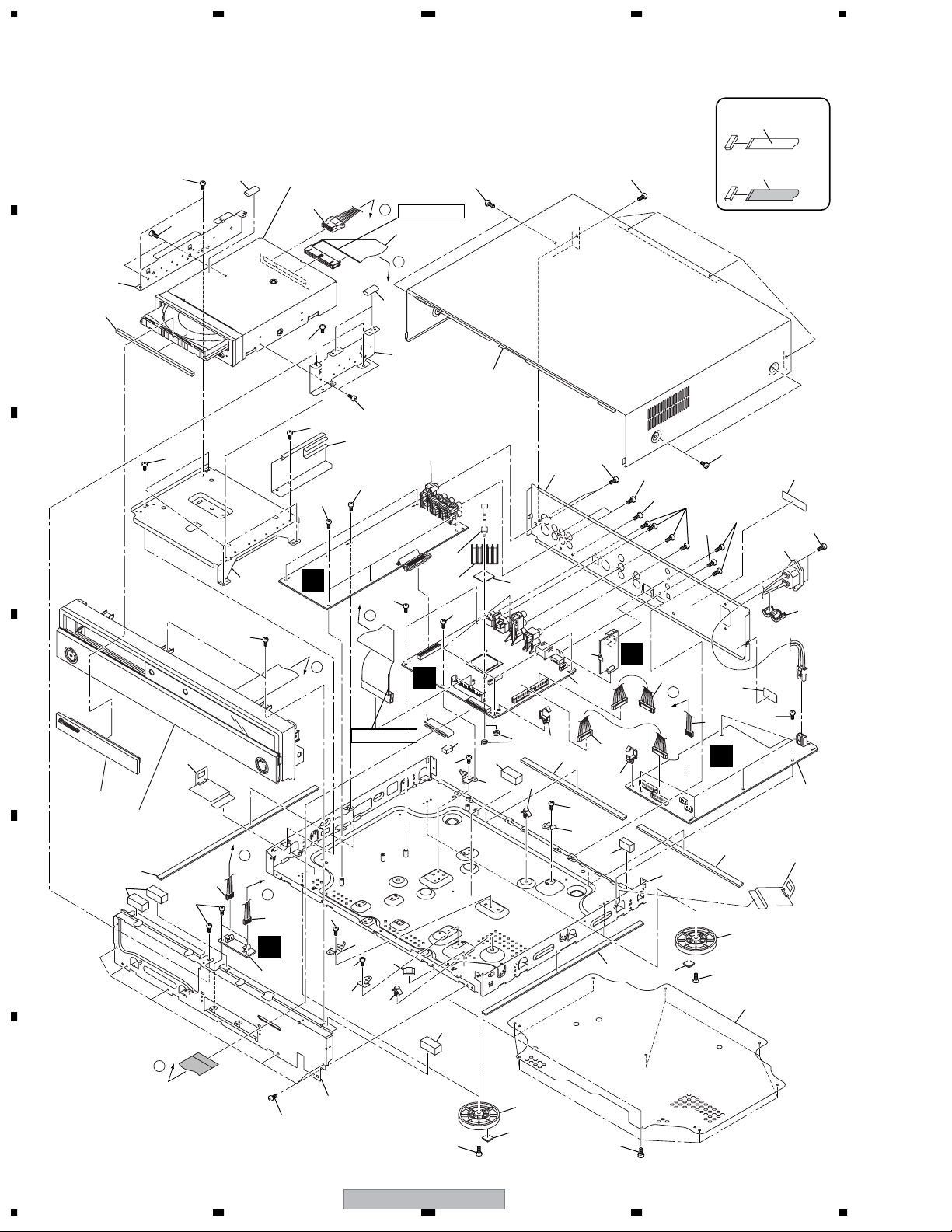
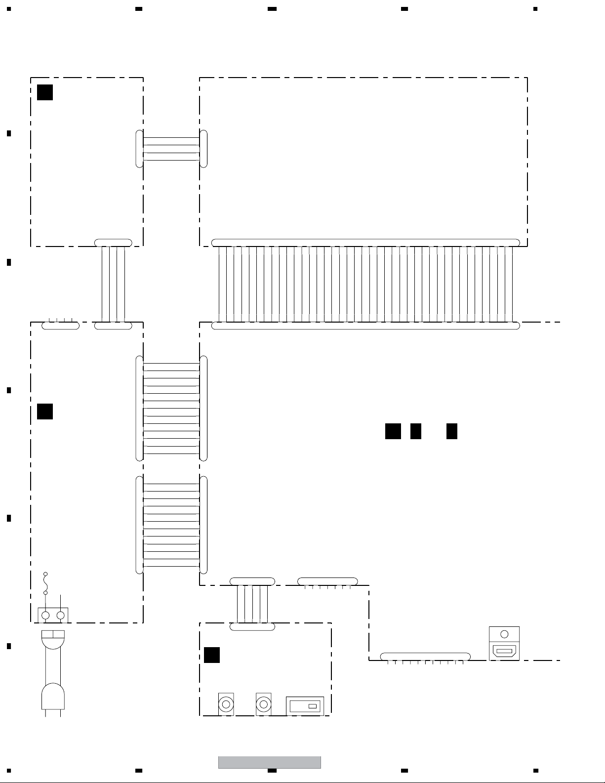
2. EXPLODED VIEWS AND PARTS LIST
NOTES:
A
2.1 PACKING
B
C
Parts marked by "NSP" are generally unavailable because they are not in our Master Spare Parts List.
The mark found on some component parts indicates the importance of the safety factor of the part.
Therefore, when replacing, be sure to use parts of identical designation.
Screws adjacent to mark on product are used for disassembly.
For the applying amount of lubricants or glue, follow the instructions in this manual.
(In the case of no amount instructions, apply as you think it appropriate.)
16
16
7
2
2
17
17
14
14
1
1
7
3
3
4
4
6
6
D
19
19
8
8
15
15
S
S
T
T
A
A
N
N
D
D
B
B
Y
Y
/
/
O
O
N
N
H
H
D
D
H
H
D
D
M
M
I
I
L
L
A
A
N
N
F
F
L
L
D
D
I
I
M
M
M
M
E
E
R
R
F
F
L
L
O
O
F
F
F
F
9
9
18
18
11
11
10
10
12
12
5
5
E
13
13
FRONT
F
8
FRONT
BDP-HD1
1234
Page 9

5 678
PACKING parts List
Mark
No. Description Part No.
1 Instruction Manual VRB1410
(English, French)
NSP 2 Warranty Card ARY1026
3 Remote Control Unit VXX3101
4 Battery Cover AZN7933
NSP 5 Bettery (R6P, AA) AEX1025
6 Nonwoven Fabric Bag VHL1108
7AC Power Cord ADG7061
>
8FRONT Pad (PS) VHA1411
9 REAR Pad (PS) VHA1412
10 Video cable VDE1065
11 Stereo audio cable VDE1064
12 Accessory Box VHC1169
13 Packing Case VHG2711
NSP 14 Polyethylene Bag(230x340) Z21-038
15 Mirror Sheet VHL1006
A
B
16 Polyethylene Bag VHL1051
17 User Card ARY1176
18 Patation Plate (Paper) VHC1170
19 Nonwoven Cloth Cover VHL1116
C
D
56
BDP-HD1
E
F
7
8
9
Page 10
1234
2.2 EXTERIOR SECTION
A
30
45
47
47
45
4
E
1
52
21
14
18
53
D
41
12
46
43
32
B
C
25
46
27
46
31
9
6
46
46
42
22
43
46
C
Red line No.1
54
B
24
33
D
42
B
A
44
28
2
11
37
46
29
13
A
20
26
40
19
46
15
16
36
39
21
17
20
46
D
Red line No.1
23
Refer to
"2.3 FRONT PANEL
SECTION".
18
19
46
E
C
6
D
F
3
5
46
36
46
30
SIDE
CONTACT SIDE
44
47
49
5
G
17
46
NON-CONTACT
50
45
51
38
35
48
7
10
46
8
23
A
34
F
10
1234
46
46
BDP-HD1
38
12
46
Page 11

>
>
5 678
EXTERIOR SECTION parts List
Mark
No. Description Part No.
1 MAIN ASSY VXX3151
2AUJB ASSY VWG2578
3 WRPB ASSY VWG2591
4 SRJB ASSY VWG2579
5 Housing ASSY (4P) VKP2388
6 Housing ASSY (4P) VKP2387
7AC Inlet ASSY ADX7523
8 SYPS ASSY VWR1402
9Drive ASSY BDR101A VXX3148
10 Filter CTX1054
11 Hold Spring VBK1168
12 Rubber Foot VEB1349
13 Radiation Sheet VEB1360
14 SYPS Rubber VEB1386
15 Rubber Spacer1 VEB1387
16 Rubber Spacer2 VEB1388
17 Spacer S VEB1392
18 Spacer R VEB1393
19 Cushion VEB1395
20 Card Spacer VEC1708
NSP 21 Clamp VEC2418
22 Styling Sheet VEC2527
23 Barrier VEC2526
24 Gasket VEC2528
25 Front Cushion VEC2538
No. Description Part No.
Mark
NSP 51 ID Label ASSY VXW1013
52 Connector ASSY PF12PP6D22
53 Connector ASSY PF13PP-D25
54 Housing ASSY (ATA) VKP2384
Service AUSR ASSY VXX3152
NSP 1..AUSR ASSY VWM2394
2..AUJB ASSY VWG2578
2..WRPB ASSY VWG2591
2..SRJB ASSY VWG2579
A
B
C
26 Small Clamp VEC2541
27 Gasket VEC2552
28 Bonnet Case S VXX3053
29 Rear Panel VNA2867
NSP 30 PCB Base VNE2378
NSP 31 Sub Chassis VNE2389
NSP 32 Writer Stay L VNE2390
NSP 33 Writer Stay R VNE2391
NSP 34 Front Stay VNE2393
NSP 35 Layer Plate VNE2394
NSP 36 PCB Stay VNE2399
37 Heatsink VNH1078
38 Insulator VNK5794
39 Stopper VNK6140
40 Ferrite Core VTX1002
NSP 41 Base Chassis ASSY VXA2743
42 Screw AMZ30P060FTC
43 Screw AMZ30P060FTC
44 Screw BBZ30P060FBN
45 Screw BBZ30P060FCC
46 Screw BBZ30P060FTC
47 Screw BPZ30P080FCC
48 Screw CBZ30P080FCC
49 Screw PCZ30P060FCC
NSP 50 Serial Label S VRW2017
D
E
F
56
BDP-HD1
7
8
11
Page 12
1234
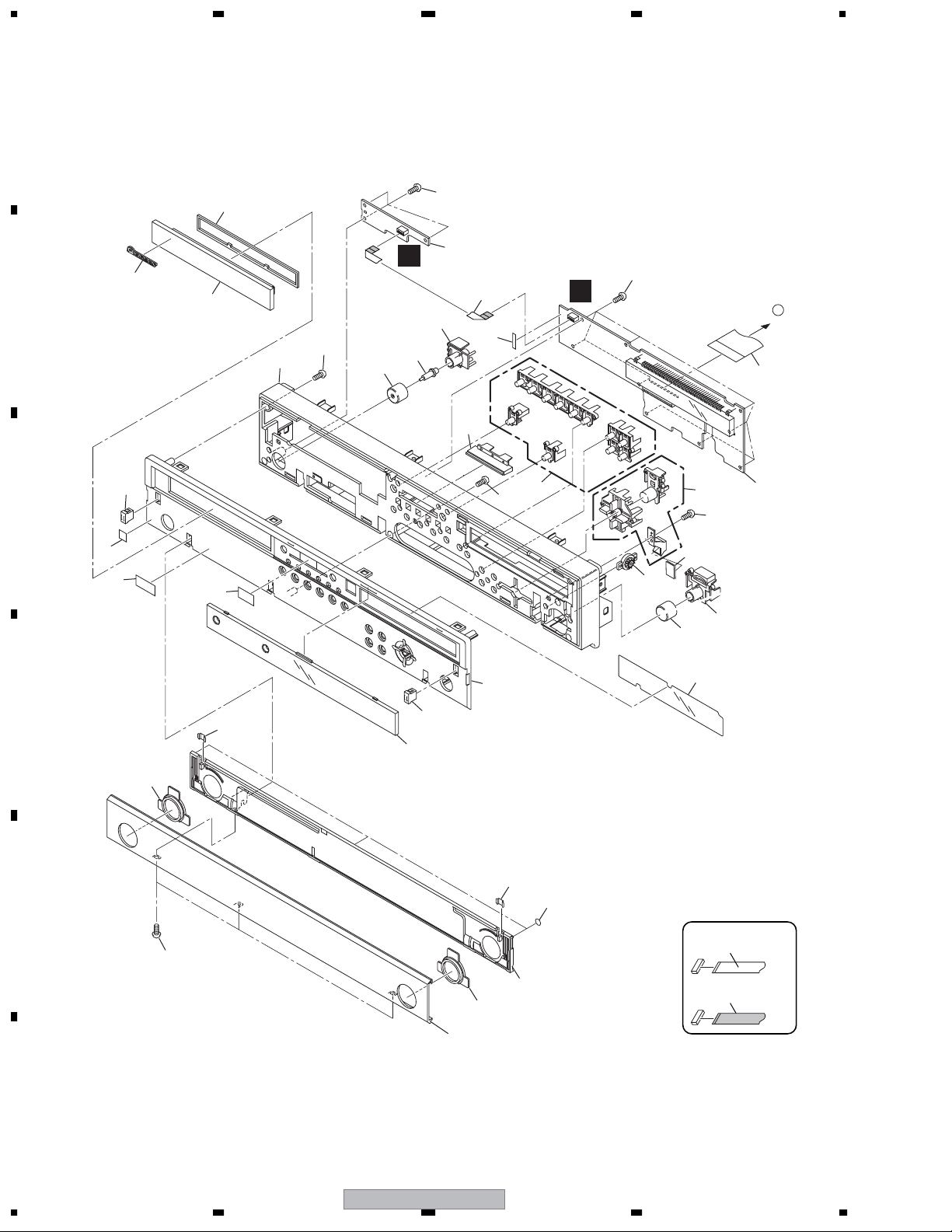
2.3 FRONT PANEL SECTION
A
C
14
26
13-1
2
12
30
26
B
8
22
26
25
Refer to
"2.2 EXTERIOR
SECTION. "
24
26
9
13-2
21
A
31
1
6
4
B
3
C
28
29
16
27
17
26
18
23
D
19
E
26
F
11
3
20
11
5
15
19
10
7
NON-CONTACT
SIDE
CONTACT SIDE
12
1234
BDP-HD1
Page 13

5 678
FRONT PANEL SECTION parts List
Mark
No. Description Part No.
1 FLKY ASSY VWG2559
2 PSWB ASSY VWG2560
3 Magnet Holder ASSY AEC1077
4 Name Plate B PAN1376
5 Rubber Sheet VEB1372
6Tray Sheet VEC2502
7 FL Filter VEC2534
8 Spacer VEC2543
9 Damper Spacer VEC2546
10 Door Panel B VNB1054
11 Magnet Catcher VNE2388
12 Illumi Lens A VNK5783
13 Power Key 1 VNK5790
14 LED Lens VNK5792
15 Door Base VNK5918
16 Tray Panel VNK5920
17 Panel Base VNK5945
18 Key Top VNK5946
19 Door Ring VNK5947
20 FL Lens VNK5948
A
B
C
21 Key Top A VNK5949
22 Main Key VNK5997
23 Front Panel VNK6015
24 Menu Key VNK6089
25 Damper ASSY VXA2504
26 Screw BPZ30P080FBN
27 Hologram Label VRW2264
NSP 28 Energy Star Label AAX8022
NSP 29 Pop Label VRW2329
30 Flexible Cable (6P) VDA2071
31 Flexible Cable (28P) VDA2152
Service FLKB ASSY VXX3153
NSP 1..FLKB ASSY VWM2357
2..FLKY ASSY VWG2559
2..PSWB ASSY VWG2560
D
E
56
BDP-HD1
F
7
8
13
Page 14
(S
)
o
T
o
T
o
T
o
T
A
1234
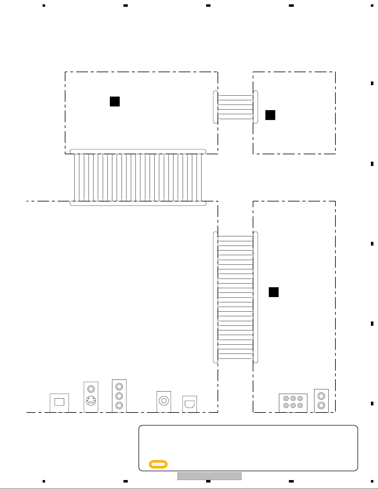
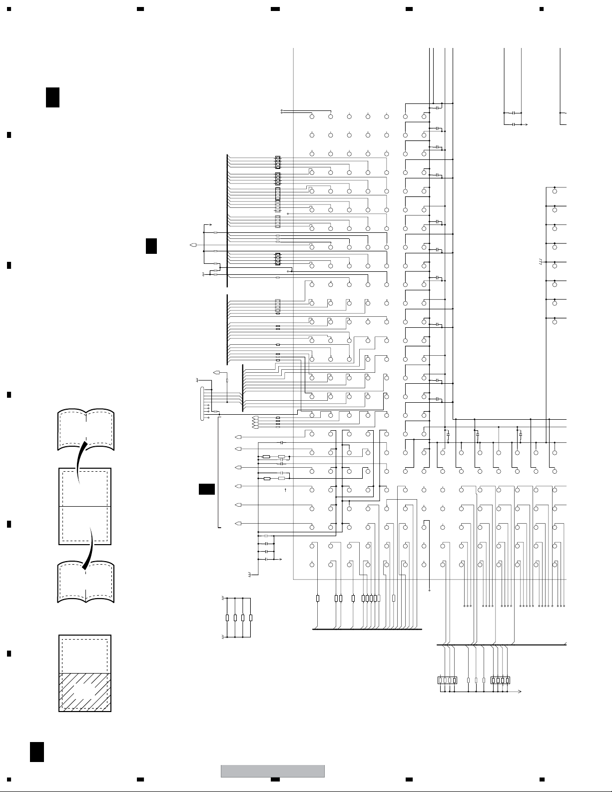
3. BLOCK DIAGRAM AND SCHEMATIC DIAGRAM
3.1 BLOCK DIAGRAM
FL
Driver
FL
B
FLKB
DRIVE
Blu
A
3LINE(A/D ports)
KEY
BD DRIVE
connector
CN3501
FLKB
connector
CN1802
ATA
A
MAIN
remote control
B
C
G
SYPS
connector
CN6002
Power
connector
CN6051
Power
27MHz
X1001
RTL8201CP
IC3001
ETHER
computer
micro
SiI9030-7
SUB
IC3601
HDMI
IC4551
1KB
I2C
BGA820pin
SMP8634
Video AMP
LA73054
IC4201
EEPROM
IC2801
Sigma Designs
IC1001
SM5302AS
Video AMP
IC4101
MEMORY
IC2701
512Mb
ATA
FLASH
256M2?
SDRAM
256M2?
SDRAM
256M2?
DDR
SDRAM
DDR
512Mbx4
IC2001,21
IC2901,21
SDRAM
DDR-0
256M2?
SDRAM
512Mbx2
IC2101,21
DDR
SDRAM
DDR-1
AMCLK, ABCLK, ALRCK, ADATA1 ,ADATA2, ADAT
DDR
25MHz
D
connector
CN2001
B to B
E
SRJB
X3001
connector
CN3501
B to B
HDMI
D
VIDEO Y,C OUT
video
OUT
VIDEO Y,C,Yp.Cb,Cr OUT
video
(HD)
OUT
OUT
D.OUT
digital
audio
B to B
CN3001
connector
connector
CN5701
B to B
D
AUJB
E
SR
IR
PCM1738
F
IC3501
audio
DAC
AUDIO C/LFE OUT
PCM1738
audio
DAC
AUDIO Ls/Rs OUT
IC3401
PCM1738
audio
DAC
AUDIO L/R/FL/FR OUT
IC3301
OU
audi
OU
OU
audi
OU
14
1234
BDP-HD1
audi
audi
Page 15
5 678
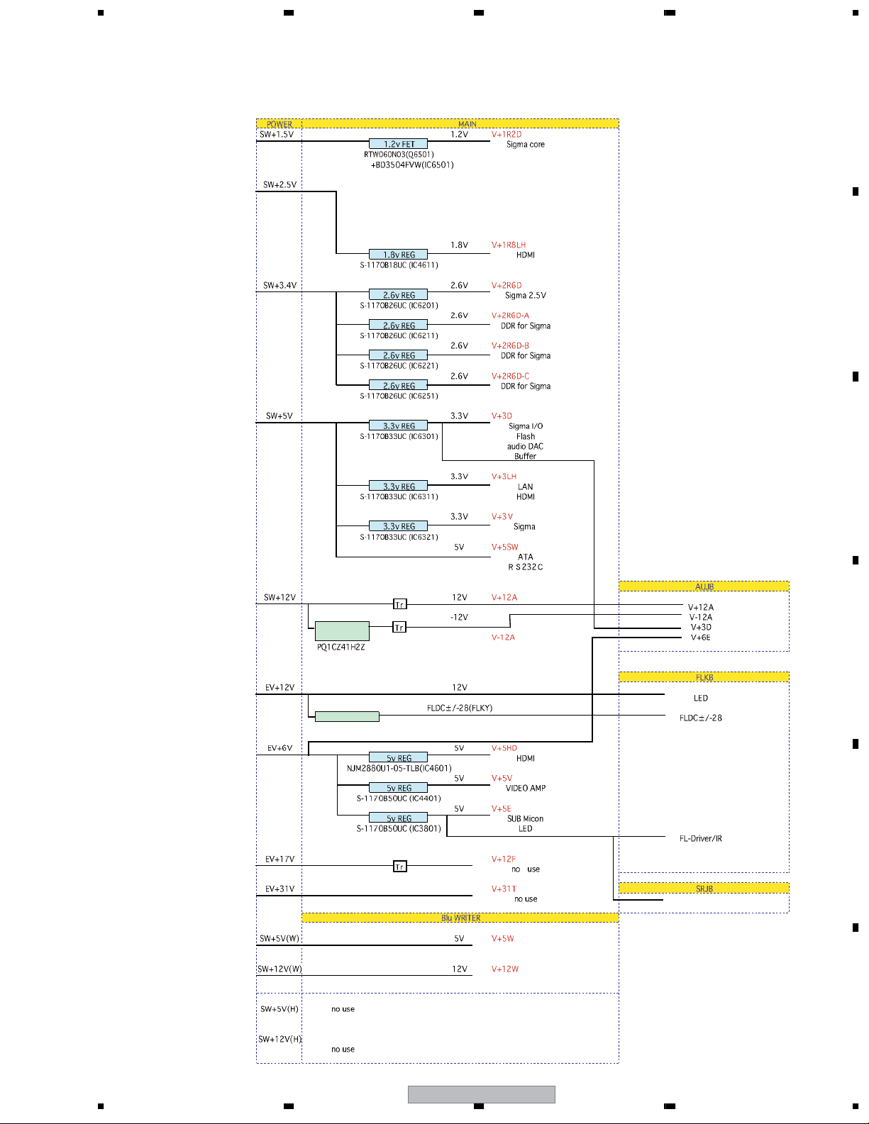
3.2 POWER BLOCK
A
B
Inversion
chopper circuitry
RCC supply circuitry
C
D
E
Blu Drive
Blu Drive
BDP-HD1
56
F
7
8
15
Page 16
1234
3.3 OVERALL WIRING DIAGRAM
A
WRPB ASSY
F
(VWG2591)
CN4002
B4B-EH
B
SW+12V
1
GND
2
GND
3
SW+5V
4
CN401
DKN1285-
1
2
3
4
BD DRIVE
CN4001
B4B-EH
2
3
4
1
GND
GND
SW+5V
SW+12V
SW+12V
GND
GND
SW+5V
1
3
4
C
2
CN204
B4B-EH-Y
YELLOW
(HDD1)
SYPS ASSY
G
(VWR1402)
D
1
2
CN203
B4B-EH
WHITE
(WRITER)
CN202
B13B-PH-K-S
CN201
B12B-PH-K-S
3
4
CN6002
P_ON
1
GND
2
EV+17V
3
GND
4
SW+5V
5
GND
6
GND
7
SW+3.4V
8
SW+3.4V
9
GND
10
GND
11
SW+2.5V
12
SW+2.5V
13
SW+1.5V
1
SW+1.5V
2
GND
3
GND
4
EV+31V
5
GND
6
EV+6V
7
GND
8
EV+12V
9
GND
10
SW+12V
11
GND
12
AKM1284-A
1
2
3
4
5
6
7
8
9
10
11
12
13
CN6051
AKM1283-A
1
2
3
4
5
6
7
8
9
10
11
12
E
CN101
LN
3-176976-4
E
37
38
39
40
GND
CS0#
CS1#
DASP#
383940
CN3401
KM200TA5
1
GND
1
CN2001
KP200TA5L
SRJB ASSY
36
DA0
DA2
36
37
345
2
GND
R_CONT
2
345
333435
DA1
PDIAG#
RESERVED
V+5E
SEL_CONT
INTRQ
(VWG2579)
AC POWER CORD
RKN1004- RKN1006-
JA2001JA2002
303132
GND
CSEL
DMACK#
30
3132333435
1234567
NC
SW
S2001
VSH1009-
272829
GND
IORDY
26
272829
RS232C
CN1861
VKN1411-A
GND
V+5SW
F
IRINSRIN
IR RECEIVER
DIOR#
NC
GND
NC
DIOW#
RXD
CN401
DKN1285-
21
2223242526
GND
DMARQ
KEYPIN
21
22
232425
CN1802
VKN2059-A
TXR
DD8
DD7
GND
123456789
RESET#
123456789
10
11
121314
151617
181920
DD6
DD9
DD5
DD4
DD3
DD2
DD1
DD0
GND
DD15
181920
A
DD14
DD12
DD13
13
14
151617
()
A 1/7–
DD10
DD11
101112
A 7/7
MAIN ASSY (VXX3151)
(VWV2234)
JA4501
AKP1278-A
JTAG,EJTAG
CN1871
VKN1415-A
123456789
V+3D
pull-up
GND
JTAG_TMS
JTAG_TDI
JTAG_RESET#
GND
JTAG_TCK
JTAG_TRST#
10
11
JTAG_TDO
pull-down
HDMI OUT
ATAPI CONNECTOR
16
SETTING1
SETTING2
BDP-HD1
1234
Page 17
5 678
A
CN3001
VKN2023-A
28
FLCLK
FLSTB
28
26
27
FLDATA
LED_STAND BY
26
27
JA4101
AKB7159-A
22
232425
KEY3
FLDC+
FL-28V
LED_STAND BY
22
232425
FLKY ASSY
B
(VWG2559)
CN101
52492-2820
161718
192021
GND
V+5E
KEY2
FLDC-
RESET_OUT
161718
192021
CN3501
52044-2845
JA4201
VKB1198-A
Y
Pb
Pr
10
1112131415
GND
LED_HD
LED_PON
LED_STAND BY
LED_HDMI
LED_Blue
1112131415
LED_LAN
10
LED_Blue
LED_STAND BY
DIGITAL AUDIO OUT
JA5501
AKB7102-A
IR
GND
KEY1
LED_FL OFF
JA5502
VKS1002-A
CN102
VKN1237-
123456789
GND
V+13E
123456789
CN5701
VKN2011-A
6
5
4
3
2
1
1
2
3
4
5
6
7
8
9
10
11
12
13
14
15
16
17
18
19
20
21
22
23
24
25
26
27
V+13E
V+5FL
RESET_OUT
KEY1_1
LED_PON
GND
XMMUTE
XAMUTE
GND
V-12A
GND
V+12A
GND
V+6E
GND
V+3D
GND
DAC_MUT
DAC_CS#
DAC_MC
DAC_MDI
DAC_MOD
GND
AMCLK
GND
ABCLK2
ADATA12
ALRCK2
DAC_RST#
DAC_CS2#
ADATA42
ADATA32
ADATA22
CN201
VKN1237-
1
2
3
4
5
6
CN3001
VKN2008-A
1
2
3
4
5
6
7
8
9
10
11
12
13
14
15
16
17
18
19
20
21
22
23
24
25
26
27
PSWB ASSY
C
(VWG2560)
AUJB ASSY
D
(VWG2578)
AUDIO OUT
5.1ch
JA3401
VKB1235-
2ch
JA3301
AKB7104-
B
C
D
E
L
R
LAN
COMPOSITE
COMPONENT
opticalCo-Axial
S-VIDEO
VIDEO OUT
÷
When ordering service parts, be sure to refer to "EXPLODED VIEWS
and PARTS LIST" or "PCB PARTS LIST".
÷
The > mark found on some component parts indicates the
importance of the safety factor of the part. Therefore, when
replacing, be sure to use parts of identical designation.
÷
: The power supply is shown with the marked box.
BDP-HD1
56
LsRsFL
Center
FRLfe
F
7
8
17
Page 18
1234
DAC
MUT
3.4 MAIN ASSY 1/7
A
A 1/7
Large size
SCH diagram
B
MAIN ASSY(VWV2234)
2
C1031
221/4
1/2
C1032
105
C1033
102
GND
C1034
221/4
R1031
0R0
C1036
106
V+1R2PLL
GND
C1035
106
GND
3
DTL1106-A
L1031
1
V+1R2S
V+1R2D
3
2
1
C1021
221/4
C1025 C1015
NM NM
C1022
105
C1023
102
GND
C1024
106
V+2R6S
V+2R6D
DTL1106-A
L1021
GND
C1011
221/4
C1012
C1013
C1014
2
105
102
106
3
DTL1106-A
1
V+3VS
GND
L1011
C1007
V+3V
R1070
0R0
106
R1002
GND
0R0
C1006
V+3USB
0R0
106
V+3PLL
GND
R1001
GND
VCH1266-AVCH1266-A
C1001
221/4
C1008C1037
C1002
C1003
C1004
221/4
C1005
105
102
106
2
3
1
V+3S
V+3D
DTL1106-A
L1001
JTAG,EJTAG IN
10
11
GND
C1874
C1875NMC1876
NM
NM
R1876
R1875
R1877
330
330
330
103
JTAG_TRST#
JTAG_TDO
NM
R1874
JTAG_TCK
R1873
330
330
JTAG_TDI
C1877NMC1872NMC1873
R1872
R1871
330
JTAG_RESET#
JTAG_TMS
123456789
1
2
3
4
1
2
3
4
R1878
R1879
103
103
VKN1415
C1871
105
CN1871
8
7
6
5
8
7
6
5
GND
R1903
R1901
0R0
C
2/2
1/2
for checker mode
Arrangement side B
V+3S
R1074
103
R1076
R1077
103
103
GND
24MHz
R1053
0R0
R1054
105
C1071
NM
C1051
C1052
120
100
X1001X1002
27MHz
VSS1205NM
R1052
105
R1089
NM
1
R1051
0R0
0R0
NM
Arrangement side A
GND
R1852
R1851
103
R1902
V+3S
V+3D
NM
A6
B6
R1078
NM
C6
D6
E6
F6
G6
H6
J6
9030_INT
for PBI_INTC
R1067
103
V+3S
RCLK1_XTAL_IN
A7
GPIO12
GPIO13
GPIO14
VDD_3V3F7
VSSG7
VDD_1V2H7
VSSJ7
PB_INT
V_MUTE
B7
C7
D7
F7
G7
H7
J7
PCI_CLK
RESET#
R1075
10
R1071
10
R1088
0R0
GND
R1055
C1081
NM
NM
R1086
R1087
R1079
103
103
NM
XTAL_OUT
RESET#
A8
RCLK0_INB9XTAL_BUF
B8
VCXO1_IN
VCXO0_IN
C8
RCLK0_OUT
RCLK1_OUT
D8
RCLK3_OUT
GPIO11
E8
VSSF8
VDD_3V3F9
F8
VDD_1V2G8
VSSG9
G8
C1116
104
XMMUTE
CLK25M
R1050
0R0
R1085
103
XTAL_IN
A9
A10
UART1_RTS
B10
UART1_DTR
C10
C9
RCLK2_OUT
D10
D9
TEST
E10
E9
VDD_3V3F10
F10
F9
VSSG10
G10
G9
JTAG_TCK
JTAG_TRST#
JTAG_TDO
JTAG_TMS
JTAG_TDI
DAC_MDO
DAC_CS2#
R1073
R1072
A11
C1115
330
UART1_RX
A12
UART0_DCD
B11
B12
UART1_CTS
C11
C12
VDD_PLL0_1V2
D11
D12
VSS_PLL0
E11
E12
VSSF12
F11
F12
VDD_1V2G12
G11
G12
VCG1063-A
330
330
UART1_TX
UART1_DSR
UART1_DCD
JTAG_UART#
XTAL_DISC
VSSF11
VDD_1V2G11
104
U0_TXR
R1058
330
UART0_TX
A13
UART0_RTS
B13
UART0_DTR
C13
VDD_PLL1_3V3
D13
VSS_PLL1
E13
VDD_3V3F13
F13
VSSG13
G13
C1103
105
DAC_CS#
R1057
UART0_RX
UART0_CTS
UART0_DSR
VDD_PLL2_3V3
VSS_PLL2
VDD_3V3F14
VSSG14
C1131
U0_RXD
A14
B14
C14
D14
E14
F14
G14
DAC_MC
_
4
3
6
5
I2C_SCL
I2C_SDA
FIP_CLK
FIP_STBIRI2CS_SDA
I2CS_SCL
FIP_DATA
D
R1062
R1061
R1064
R1063
R1081
R1082
R1083
R1084
330
330
330
330
330
330
330
330
R1066
103
VI1_CLK
VI1_P0
NCA1
A2
A1
VI1_P4B2VI1_P1B3VI1_HS
B1
VI1_P5C2VI1_P6C3VI1_P2C4VI1_P3
C1
E
VI0_P0D3VI1_P7
VI0_P1
D2
D1
VI0_P3E3VI0_P2
VI0_P4
E1
E2
VI0_P9F2VI0_P8F3VI0_P7F4VI0_P6F5VI0_P5
F1
VI0_P14G2VI0_P13G3VI0_P12G4VI0_P11G5VI0_P10
G1
VI0_P19H2VI0_P18H3VI0_P17H4VI0_P16H5VI0_P15
H1
VI0_HS
VI0_VS
J1
VI1_VS
A3
VI1_VLD
GPIO4
GPIO5E5GPIO6
VI0_P22J4VI0_P21J5VI0_P20
J3
J2
A4
B4
RCLK1_XTAL_OUT
GPIO0
A5
GPIO1
GPIO7
B5
GPIO8
GPIO2
C5
GPIO9
GPIO3
D4
D5
GPIO10E7GPIO15
E4
VSSF6
VDD_3V3G6
VSSH6
VDD_3V3J6
F
18
1234
BDP-HD1
Page 19
B11
C11
D11
G
5 678
A
EJTAG IN
C1877NMC1872NMC1873
C1874
NM
R1873
R1872
R1871
R1874
330
330
330
330
JTAG_RESET#
JTAG_TCK
JTAG_TMS
JTAG_TDI
GND
R1903
0R0
0R0
NM
Arrangement side A
GND
R1852
R1851
103
JTAG_TCK
JTAG_TRST#
JTAG_TDO
JTAG_TMS
JTAG_TDI
DAC_MDO
R1058
330
R1901
NM
U0_TXR
330
1234567
R1878
103
1
2
3
4
1
2
3
4
R1879
103
R1902
DAC_CS#
R1057
CN1871
VKN1415
C1871
105
8
7
6
5
8
7
6
5
V+3S
V+3D
U0_RXD
DAC_MC
DAC_MUT
3
658
V+3D
DAC_MDI
214
330
7
W.Reset
R1056
GND
IDE_D9
IDE_D8
IDE_D7
IDE_D5
R1861
103
R1862
103
IDE_D6
IDE_D10
IDE_D11
IDE_D4
RS232C IN
R1864
R1865
V+5SW
330
330
U0_RXD
U0_TXR
IDE_D12
IDE_D2
IDE_D3
IDE_D13
IDE_D14
IDE_D0
IDE_D15
IDE_D1
IDE_DMARQ
IDE_DIOW#
1234567
C1861
105
IDE_DMACK#
IDE_DIOR#
IDE_IORDY
CN1861
VKN1411
IDE_PA0
IDE_PA2
IDE_IRQ
IDE_PA1
GND
IDE_CS0#
IDE_CS1#
IDE_CBLID#
NM
R1827
DRAM1_D12
DRAM1_D13
DRAM1_D14
DRAM1_D15
VKN2059-A
CN1802
103
R1826
DRAM1_D10
DRAM1_D11
DRAM1_D9
TP3001
TP3002
D1801
NM
DRAM1_DM0
DRAM1_DM1
DRAM1_DQS1
DRAM1_DQS0
DRAM1_D8
GND
40
NM
DASP#
CS1#
R1825
DRAM1_D5
DRAM1_D6
DRAM1_D7
CS0#
DA2
3637383940
35
R1824
330
6587
2143
IDE_CS0#
IDE_CS1#
IDE_PA2
DRAM1_D3
DRAM1_D1
DRAM1_D0
DRAM1_D4
PDIAG#
DA0
470
IDE_PA0
VCG1063-A
GND
DRAM1_D2
DRAM1_CLK
To BD WRITER Primary ATA
RESERVED
DA1
C1821
NM
NM
R1828
R1829
R1830
R1823
820
330
330
IDE_CBLID#
IDE_PA1
C1204
104
C1205
C1206
104
DRAM1_D31
DRAM1_D30
DRAM1_D29
DRAM1_CLKN
DRAM1_D28
INTRQ
GND
103
R1821
220
IDE_IRQ
VREFD-B
DRAM1_D25
DRAM1_D24
DRAM1_DQS3
DMACK#
CSEL
R1836
0R0
R1822
R1820
820
IDE_DMACK#
DRAM1_D22
DRAM1_D23
DRAM1_D26
DRAM1_D27
IORDY
DIOR#
GND
R1819
102
R1818
220
IDE_IORDY
R1807
223
DRAM1_CLKE
DRAM1_DM2
DRAM1_DM3
DRAM1_DQS2
DIOW#
GND
R1816
R1817
220
IDE_DIOR#
IDE_DIOW#
IDE_PA1
IDE_PA0
IDE_PA2
6587
R1806
223
DRAM1_D20
DRAM1_D21
DRAM1_D19
DRAM1_D17
DRAM1_D18
DMARQ
GND
21222324252627282930313233343536373839
562
R1815
820
IDE_DMARQ
IDE_CS0#
IDE_CS1#
2143
DRAM1_A12
DRAM1_A9
DRAM1_WE
DRAM1_A11
KEYPIN
R1814
43
DRAM1_A13
DD15
GND
19
R1834
NM
V+3D
R1813
IDE_D15
IDE_DIOR#
IDE_DIOW#
IDE_DMACK#
6587
21
R1805
223
DRAM1_A8
DRAM1_A7
DRAM1_A6
DRAM1_CS
DRAM1_RAS
DRAM1_D16
DD14
DD0
330
6587
2143
IDE_D14
IDE_D0
IDE_D15
43
DRAM1_CAS
DRAM1_A5
DD1
IDE_D1
IDE_D0
6587
R1804
223
DRAM1_BA1
DRAM1_A4
DRAM1_A10
DD13
DD2
13
1415161718
R1812
330
6587
IDE_D13
IDE_D2
IDE_D14
IDE_D1
21
DRAM1_BA0
DRAM1_A3
DD12
DD3
2143
IDE_D12
IDE_D3
IDE_D13
IDE_D2
6587
43
R1803
223
DRAM1_A1
DRAM1_A0
DRAM1_A2
DD11
10111213141516171819202122232425262728293031323334
DD4
101112
R1811
330
6587
IDE_D11
IDE_D4
IDE_D12
IDE_D3
21
DD10
DD5
2143
IDE_D10
IDE_D5
IDE_D4
IDE_D11
6587
43
R1802
223
DD9
R1810
IDE_D9
IDE_D10
21
DD6
DD8
330
6587
2143
IDE_D6
IDE_D5
43
DD7
IDE_D8
IDE_D7
IDE_D6
IDE_D9
6587
R1801
223
GND
GND
123456789
123456789
R1809
562
330
IDE_D8
21
RESET#
CN1803
NM
R1808
AUX_RESET#
IDE_D7
R1835
NM
C1801
105
C1802
105
223
R1833
R1832
B
C
R1831
V+3D
V+5SW
0R0
NM
D
UART1_RX
UART0_TX
UART0_RX
A13
A12
UART0_DCD
UART0_RTS
UART0_CTS
B13
B12
UART1_CTS
UART0_DTR
UART0_DSR
C13
C12
VDD_PLL0_1V2
VDD_PLL1_3V3
VDD_PLL2_3V3
D13
D12
VSS_PLL1
VSS_PLL0
E11
E12
VSSF12
F11
F12
VDD_1V2G12
11
G12
VCG1063-A
VDD_3V3F13
F13
VSSG13
G13
C1103
VSS_PLL2
E13
E14
VDD_3V3F14
F14
VSSG14
G14
C1131
105
SCARD_CLK
SCARD_IO
A15
A14
SCARD_RST
SCARD_FC#
B14
B15
SCARD_CTL0
IDE_D8
C14
C15
SCARD_CTL1
VDD_PLL3_3V3
D14
D15
SCARD_CTL2
VSS_PLL3
E15
VSSF15
VSSF16
F15
VDD_1V2G16
VDD_1V2G15
G15
C1130
105
IDE_D12
IDE_D6
A16
IDE_D10
B16
IDE_D5
C16
IDE_D7
D16
IDE_D9
E16
VDD_3V3F17
F16
VSSG17
G16
IDE_D1
A17
A18
IDE_D15
IDE_D3
B17
B18
IDE_D13
IDE_D0
C17
C18
IDE_D11
IDE_D2
D17
D18
IDE_D14
IDE_D4
E17
E18
VSSF19
VDD_3V3F18
F17
F18
VDD_1V2G19
VSSG18
G17
G18
A19
B19
C19
D19
E19
F19
G19
IDE_IOR#
IDE_IORDY
IDE_ACK#
IDE_DMARQ
IDE_IOW#
VSSF20
VDD_1V2G20
VCG1063-A
C1102
IDE_NPCBLID
A20
A21
IDE_A0
B21
B20
IDE_A2
C21
C20
IDE_IRQ
D21
D20
IDE_A1
E20
E21
VSSF21
F20
F21
VDD_1V2G21
G20
G21
104
DRAM1_DQ13
DRAM1_DQ14
DRAM1_DQ15
IDE_CS0#
IDE_CS1#
VDD_2V5F22
VSSG22
C1114
A22
B22
C22
D22
E22
F22
G22
105
DRAM1_DQ9
DRAM1_DQ10
DRAM1_DQ11
DRAM1_DQ12
DRAM1_VREFSSTL2
VDD_2V5F23
VDD_1V2G23
C1129
A23
B23
C23
D23
E23
F23
G23
DRAM1_DM0
DRAM1_DM1
DRAM1_DQ8
DRAM1_DQS1
VSSF24
VDD_1V2G24
104
C1113
A24
B24
C24
D24
E24
F24
G24
DRAM1_DQ4
A25
DRAM1_DQ5
B25
DRAM1_DQ6
C25
DRAM1_DQ7
D25
DRAM1_VREFSSTL1
E25
VDD_2V5F25
F25
VSSG25
G25
DRAM1_CK
DRAM1_DQ2
DRAM1_DQ3
DRAM1_DQ0
DRAM1_DQ1
VSSF26
VSSG26
VCG1063-A
DRAM1_DQS0
DRAM1_DQ27
DRAM1_CK#
A26
B26
C26
D26
E26
F26
G26
C1101
A27
DRAM1_DQ31
B27
DRAM1_DQ30
C27
DRAM1_DQ28
D27
DRAM1_DQ29
E27
VDD_2V5F27
F27
VDD_1V2G27
G27
C1140
105
A28
DRAM1_DQ26
B28
DRAM1_DQ25
C28
DRAM1_DQS3
D28
DRAM1_DQ24
E28
DRAM1_VREFSSTL0
F28
VSSG28
G28
VDD_1V2H28
H28
VSSJ28
J28
DRAM1_DM3
A29
DRAM1_DM2
B29
DRAM1_DQS2
C29
DRAM1_DQ22
D29
DRAM1_DQ23
E29
VDD_2V5F29
F29
DRAM0_VREFSSTL2
G29
VDD_2V5H29
H29
VSSJ29
J29
DRAM1_DQ21
A30
DRAM1_DQ20
B30
DRAM1_DQ19
C30
DRAM1_DQ17
D30
DRAM1_DQ18
E30
DRAM1_CKE
DRAM0_DQS1
DRAM0_VREFSSTL1
F30
DRAM0_DQ12
G30
H30
J30
DRAM1_DQ16
A31
DRAM1_A13
B31
DRAM1_WE#
C31
DRAM1_A9
D31
DRAM1_A11
E31
DRAM1_A12
F31
DRAM0_DQ13
G31
DRAM0_DQ8
H31
DRAM0_DQ7
J31
DRAM1_CAS#
DRAM1_RAS#
DRAM1_CS#
DRAM1_A6
DRAM1_A7
DRAM1_A8
DRAM0_DQ11
DRAM0_DM1
DRAM0_DQ6
DRAM1_BA0
NCA34
A32
A33
A34
DRAM1_BA1
DRAM1_A0
B32
B33
B34
DRAM1_A10
DRAM1_A1
C33
C32
D32
E32
F32
G32
H32
J32
DRAM1_A4
D33
DRAM1_A5
E33
DRAM0_DQ15
F33
DRAM0_DQ10
G33
DRAM0_DM0
H33
DRAM0_DQ5
J33
C34
DRAM1_A2
D34
DRAM1_A3
E34
DRAM0_DQ14
DRAM0_DQ9
DRAM0_DQS0
DRAM0_DQ4
E
DRAM0_D15
F34
G34
H34
J34
DRAM0_D14
DRAM0_D12
DRAM0_D13
DRAM0_D11
DRAM0_D10
DRAM0_D9
DRAM0_DQS1
DRAM0_D8
DRAM0_DM1
DRAM0_DM0
DRAM0_DQS0
DRAM0_D7
DRAM0_D6
DRAM0_D5
DRAM0_D4
DRAM0_D1
DRAM0_D0
C1201
VREFD-A
104
F
56
BDP-HD1
7
8
19
Page 20
1
G
1234
A
A 1/7
B
C
SCH diagram
D
E
MAIN ASSY(VWV2234)
A 5/7
Large size
1/2
2/2
PCLK
GND
CN1893
NM
GND
9030_RST#
10
9
8
7
6
5
4
3
2
1
for PBI_INTC
V+3S
R1407
103
R1409
103
R1418
NM
R1419
103
R1412
103
R1315
103
A 5/7
GND GNDV
NM
AUX_RESET#
SVid-Y
SVid-C
CVBS
Pr/R
Pb/B
VO_P19
VO_P20
VO_P21
VO_P22
VO_P23
VO_P14
VO_P15
VO_P16
VO_P17
VO_P18
VO_P9
VO_P10
VO_P11
VO_P12
VO_P13
VO_P5
VO_P6
VO_P7
VO_P8
STBY_DSCL
VO_P3
VO_P4
VRDY
STBY_DSDA
VO_P1
VO_P2
VO_VS
VO_HS
STBY_HPDET
VO_P0
ETH_TXD3
ETH_TXD2
ETH_TXD1
ETH_TXD0
ETH_MDIO
ETH_MDINT#
ETH_TXC
ETH_TXEN
ETH_CRS
ETH_RXD1
ETH_RXD2
ETH_RXD3
ETH_COL
ETH_RXC
ETH_RXD0
ETH_MDC
ETH_RXDV
ETH_RXERR
R1316
LED7
LED4
LED3
LED2
1080P
XAMUTE
DAC_RST#
Y/G
VCG1063-A
R1428
R1429
0R0
0R0
C1425
C1426
C1427
C1428
GNDV
R1427
0R0
LED11
LED10
LED9
LED8
LED7
LED6
LED5
LED4
LED3
LED2
LED1
104
104
105
R1426
0R0
R1414
R1415
R1416
330
R1413
R1302
R1304
R1305
R1307
R1308
R1309
R1310
R1311
R1312
R1313
R1314
R1421
1300
C1423
C1422
C1424
R1422
1300
10 Ω is J %
R1301
C1421
220
R1423
R1424
330
330
330
220
220
220
220
220
220
220
220
220
220
220
104
100
100
V+3VS
R1401
330
R1402
330
R1403
330
R1404
330
R1406
330
R1410
330
822
104
822
VI0_VLDK3VI0_P25
VI0_CLK
K1
K2
VI2_VSL2VI2_HS
L1
VI2_CLKM2VI2_VLDM3VI0_P31
M1
VO0_P22
VO0_P21N4VO0_P20
VO0_P23
N1
N2
VO0_P16
VO0_P18
VO0_P17
P1
P2
VO0_P11
VO0_P12
VO0_P13
R1
R2
VO0_P7T3VO0_P6
VO0_P8
T1
T2
VO0_CLK
VO0_VLD
U1
U2
VO0_VS
VO0_HS
V1
V2
ETH_TXD3
NCW2
W2
W1
ETH_TXD2
ETH_TXD1
Y1
Y2
ETH_TXCLK
ETH_TX_EN
AA1
AA2
ETH_RXD3
ETH_RXD2
AB1
AB2
ETH_RXCLK
ETH_RXD0
AC1
AC2
ETH_MDC
GPIO27
GPIO26
AD1
AD2
ETH_RX_DV
GPIO23
GPIO22
AE1
AE2
ETH_RX_ER
GPIO19
AF2
AF1
VO1_AVDD_Y
VO1_Y
AG1
AG2
VO1_AVDD_V
VO1_V
AH1
AH2
VO1_AVDD_U
VO1_U
AJ1
AJ2
VO2_AVDD_Y
VO2_Y
AK1
AK2
VO2_AVDD_V
VO2_V
AL2
AL1
VO2_AVDD_U
VO2_U
AM1
AM2
SO0_LRCLK
SO0_SPDIF
AN2
AN1
SO0_MCLK
NCAP1
AP2
AP1
R1506
R1507
R1508
220
220
220
SPDIF0
ALRCLK
AMCLK
VI0_P28
L3
N3
P3
R3
VO0_P0
ETH_RXD1
AB3
ETH_COL
AC3
GPIO18
VO1_AVSS_Y
VO1_AVSS_V
VO1_AVSS_U
VO2_AVSS_Y
VO2_AVSS_V
AL3
VO2_AVSS_U
AM3
SO0_DATA2
AN3
SO0_BCLK
AP3
VO0_P4
U3
VO0_P2
V3
W3
ETH_TXD0
Y3
ETH_CRS
AA3
AD3
AE3
AF3
AG3
AH3
AJ3
AK3
R1505
220
ABCLK
VO0_P15
VO0_P10
VO0_P5
GPIO25
GPIO21
VI0_P24
VI0_P27
VI0_P30
P4
R4
T4
GPIO31
GPIO17
VO1_AVDD
VO1_RSET
VO2_RSET
VO2_AVDD
SO0_DATA5
AL4
SO0_DATA4
AM4
SO0_DATA3
AN4
SO0_DATA1
AP4
R1503
R1504
220
220
ADATA1
ADATA2
K4
L4
M4
VO0_P3
U4
VO0_P1
V4
HDMI_HPD
W4
ETH_MDIO
Y4
NCAA4
AA4
AB4
GPIO29
AC4
AD4
AE4
AF4
AG4
AH4
AJ4
AK4
R1502
220
ADATA3
VO0_P19
VO0_P14
R1501
R1509
220
220
ADATA4
ADATA5
VI0_P23
VI0_P26
VI0_P29
N5
P5
VO0_P9
GPIO24
GPIO20
GPIO16
VO1_AVSS
VO1_VREF
VO2_VREF
VO2_AVSS
SO1_DATA5
SO1_SPDIF
AM5
SO1_BCLK
AN5
SO1_MCLK
AP5
AMCLK1
K5
L5
M5
R5
HDMI_PD#
T5
HDMI_DSCL
U5
HDMI_DSDA
V5
HDMI_MSEN
W5
NCY5
Y5
ETH_MDINT#
AA5
GPIO30
AB5
GPIO28
AC5
AD5
AE5
AF5
AG5
AH5
AJ5
AK5
AL5
R1510
220
ABCLK1
SPDIF1
VDD_3V3K6
K6
VSSL6
L6
VSSM6
M6
VDD_3V3N6
N6
VDD_3V3P6
P6
VDD_3V3V6
VDD_3V3AA6
VDD_3V3AB6
VSSAC6
VSSAD6
VDD_3V3AE6
VDD_3V3AF6
VSSAG6
VSSAH6
VSSAJ6
SO1_LRCLK
SO1_DATA4
SO1_DATA2
SO1_DATA3
SO1_DATA1
ADATA11
ALRCK1
VSSR6
VSST6
VDD_3V3U6
U6
V6
VSSW6
VSSY6
AA6
AB6
AC6
AD6
AE6
AF6
AG6
AH6
AJ6
AK6
AL6
AM6
AN6
AP6
ADATA31
ADATA21
R6
T6
W6
Y6
ADATA41
VSSK7
K7
VDD_1V2L7
L7
VDD_1V2M7
M7
VSSN7
N7
VSSP7
VDD_1V2R7
VDD_1V2T7
VSSU7
VSSV7
VDD_1V2W7
VDD_1V2Y7
VSSAA7
VSSAB7
VDD_1V2AC7
VDD_1V2AD7
AD7
VSSAE7
VSSAF7
VDD_1V2AG7
VSSAH7
AH7
VSSAJ7
SI1_LRCLK
SI0_LRCLK
SI0_SPDIF
AM7
SI0_BCLK
AN7
SI0_DATA
AP7
ADATA51
P7
R7
T7
U7
V7
W7
Y7
AA7
AB7
AC7
VCG1063-A
AE7
AF7
AG7
AJ7
AK7
AL7
C1132
105
C1117
104
C1104
VCG1063-A
C1118
104
C1119
104
C1105
VCG1063-A
C1133
105
C1120
104
C1106
C1134
105
VDD_1V2AH8
VSSAJ8
SI1_SPDIF
SI1_BCLK
SI1_DATA
PCI_INTA#
PCI_CLK
104
AP8
AH8
AJ8
AK8
AL8
AM8
AN8
PCI_CLK
C1121
VSSAH9
VDD_3V3AJ9
PCI_REQ1#
PCI_REQ0#/GNT#
PCI_GNT3#
PCI_GNT1#
PCI_GNT0#/REQ#
PCI_INTA#
AH9
AJ9
AK9
AL9
AM9
AN9
AP9
PCI_GNT#0
104
VSSAH10
VDD_3V3AJ10
PCI_GNTB3
PCI_GNTB1
PCI_REQ0#
C1122
AH10
AJ10
PCI_REQ2#
AK10
PCI_AD28
AL10
PCI_GNT2#
AM10
PCI_AD29
AN10
PCI_AD31
AP10
PCI_AD29
PCI_AD31
PCI_GNTB2
PCI_REQ1#
VDD_1V2AH11
VSSAJ11
AK11
AL11
PCI_AD30
AM11
PCI_AD25
AN11
PCI_AD27
AP11
PCI_AD28
PCI_REQ2#
C1153
VCG1063-A
C1154
105
AH11
AJ11
PCI_REQ3#
PCI_AD24
PCI_AD27
PCI_AD25
PCI_AD30
VCG1063-A
VDD_1V2AH12
VSSAJ12
PCI_IDSEL2
PCI_IDSEL1
PCI_AD26
PCI_AD23
PCI_CBE3#
AP12
PCI_AD24
PCI_REQ3#
V+1R2PLL
C1107
AH12
AJ12
AK12
AL12
AM12
AN12
PCI_CBE3#
PCI_AD26
PCI_AD23
GND
VSSAH13
AH13
VDD_3V3AJ13
AJ13
AK13
PCI_IDSEL3
AL13
PCI_AD20
AM13
PCI_IDSEL0
AN13
PCI_AD21
PCI_AD19
AP13
PCI_IDSEL2
PCI_IDSEL1
PCI_AD19
PCI_IDSEL0
PCI_AD20
PCI_AD21
VSSP14
P14
VSSR14
R14
VSST14
T14
VSSU14
U14
VSSV14
V14
VSSW14
W14
VSSY14
Y14
VSSAA14
AA14
VSSAH14
VDD_3V3AJ14
PCI_AD18
PCI_FRAME#
PCI_AD22
PCI_CBE2#
PCI_AD17
AP14
PCI_IDSEL3
C
VC
C
AH14
AJ14
AK14
AL14
AM14
AN14
PCI_CBE2#
PCI_AD22
PCI_AD17
F
A 1/7
20
PCI_REQ3#
PCI_REQ1#
PCI_REQ0#
PCI_INTA#
PCI_REQ2#
R1894
R1895
R1893
103
103
103
PCI_FRAME#
R1892
103
PCI_TRDY#
PCI_DEVSEL#
PCI_STOP#
PCI_IRDY#
R1891
103
V+3S
2/2
1234
BDP-HD1
Page 21

J
PCI REQ3#
PCI AD24
5 678
A
VDD_2V5K29
DRAM0_DQ1
DRAM0_DQ0
DRAM0_DQ3
DRAM0_DQ2
K32
L32
M32
N32
P32
DRAM0_WE#
R32
DRAM0_CS#
T32
DRAM0_A10
U32
DRAM0_A2
V32
NCW32
W32
NCY32
Y32
NCAA32
AA32
TS1_IN_SYNC
AB32
TS1_IN_D4
AC32
TS1_IN_D5
AD32
TS0_IN_D2
AE32
TS0_IN_D3
AF32
PB_CS2#
AG32
AH32
AJ32
AK32
AL32
AM32
AN32
PB_A1
PB_A2
PB_A0
K33
DRAM0_DQ31
L33
DRAM0_DQ26
M33
DRAM0_DM2
N33
DRAM0_DQ20
P33
DRAM0_A13
R33
DRAM0_RAS#
T33
DRAM0_BA1
U33
DRAM0_A1
V33
NCW33
NCY33
TS0_IN_D0
TS0_IN_D1
PB_CS1#
PB_AD9
PB_AD13
PB_AD1
AK33
PB_AD5
AL33
PB_DMAACK#
AM33
PB_DMARQ
AN33
PB_IORDY
AP33
W33
Y33
NCAA33
AA33
TS1_IN_D1
AB33
TS1_IN_D2
AC33
TS1_IN_D3
AD33
AE33
AF33
AG33
AH33
AJ33
PB_IORDY
PB_DMARQ
DRAM0_CK
DRAM0_CK#
DRAM0_DQ27
DRAM0_DM3
DRAM0_DQ21
DRAM0_DQ16
DRAM0_CAS#
DRAM0_BA0
U34
DRAM0_A0
V34
TS0_IN_SYNC
TS0_CLK
PB_CS0#
PB_AD8
PB_AD12
PB_AD0
PB_AD4
PB_RD#
PB_WR#
AN34
NCAP34
AP34
K34
L34
M34
N34
P34
R34
T34
NCW34
W34
NCY34
Y34
NCAA34
AA34
NCAB34
AB34
TS1_CLK
AC34
TS1_IN_D0
AD34
AE34
AF34
AG34
AH34
AJ34
AK34
AL34
AM34
PB_RD#
PB_WR#
GND
AH13
AJ13
AK13
PCI_IDSEL3
AL13
PCI_AD20
AM13
PCI_IDSEL0
AN13
PCI_AD21
PCI_AD19
AP13
PCI_AD19
PCI_IDSEL0
PCI_AD20
PCI_AD21
VSSP14
P14
VSSR14
R14
VSST14
T14
VSSU14
U14
VSSV14
V14
VSSW14
W14
VSSY14
Y14
VSSAA14
AA14
VSSAH14
AH14
VDD_3V3AJ14
AJ14
AK14
PCI_AD18
AL14
PCI_FRAME#
AM14
PCI_AD22
AN14
PCI_CBE2#
PCI_AD17
AP14
PCI_IDSEL3
PCI_AD17
C1151
VCG1063-A
C1152
105
VSSAJ15
PCI_CBE2#
PCI_AD22
PCI_FRAME#
VSSP15
P15
VSSR15
R15
VSST15
T15
VSSU15
U15
VSSV15
V15
VSSW15
W15
VSSY15
Y15
VSSAA15
AA15
105
VDD_1V2AH15
AH15
AJ15
AK15
PCI_AD16
AL15
PCI_TRDY#
AM15
PCI_IRDY#
AN15
PCI_STOP#
PCI_DEVSEL#
AP15
PCI_AD18
V+3PLL
VSSP16
VSSR16
VSST16
VSSU16
VSSV16
VSSW16
VSSY16
VSSAA16
C1135
VDD_1V2AH16
VSSAJ16
PCI_AD16
PCI_DEVSEL#
PCI_TRDY#
PCI_IRDY#
PCI_STOP#
P16
R16
T16
U16
V16
W16
Y16
AA16
AH16
AJ16
AK16
PCI_AD15
AL16
PCI_AD13
AM16
PCI_PAR
AN16
PCI_AD14
PCI_CBE1#
AP16
PCI_CBE1#
PCI_AD13
PCI_AD14
PCI_PAR
VSSP17
VSSR17
VSST17
VSSU17
VSSV17
VSSW17
VSSY17
VSSAA17
PCI_AD4
PCI_AD11
PCI_AD12
PCI_AD10
PCI_AD8
AP17
PCI_AD15
P17
R17
T17
U17
V17
W17
Y17
AA17
VCG1063-A
VSSAH17
AH17
VDD_3V3AJ17
AJ17
AK17
AL17
AM17
AN17
PCI_AD10
PCI_AD12
PCI_AD8
VSSP18
VSSR18
VSST18
VSSU18
VSSV18
VSSW18
VSSY18
VSSAA18
C1108
PCI_AD6
PCI_CBE0#
PCI_AD9
PCI_AD7
PCI_AD5
AP18
PCI_AD11
PCI_AD4
P18
R18
T18
U18
V18
W18
Y18
AA18
VSSAH18
AH18
VDD_3V3AJ18
AJ18
AK18
AL18
AM18
AN18
PCI_AD9
PCI_AD7
PCI_AD5
VSSP19
P19
VSSR19
R19
VSST19
T19
VSSU19
U19
VSSV19
V19
VSSW19
W19
VSSY19
Y19
VSSAA19
AA19
VDD_1V2AH19
VSSAJ19
AK19
PCI_AD2
AL19
PCI_AD0
AM19
PCI_AD3
AN19
PCI_AD1
AP19
USB20_XO
PCI_CBEO#
PCI_AD6
AH19
AJ19
PCI_AD1
PCI_AD0
PCI_AD3
VSSP20
P20
VSSR20
R20
VSST20
T20
VSSU20
U20
VSSV20
V20
VSSW20
W20
VSSY20
Y20
VSSAA20
AA20
C1136
105
VDD_1V2AH20
AH20
VSSAJ20
AJ20
USB20_VSSAT_0AK20
AK20
USB20_VSSAT_0AL20
AL20
USB20_VDDAT_0_3V3AM20
AM20
AN20
USB20_REXT
AP20
USB20_XI
PCI_AD2
332
GND
VSSP21
P21
MAIN LSI
VSSR21
VSST21
VSSU21
VSSV21
VSSW21
VSSY21
VSSAA21
R21
T21
U21
V21
W21
Y21
AA21
(SMP8634LF)
V+3USB
105
C1161
VCG1063-A
C1162
VCG1063-A
C1123
VSSAH22
AH22
VDD_3V3AJ22
AJ22
USB20_VSSAT_1AK22
AK22
USB20_VDDAC_3V3
AL22
USB20_VDDAT_1_3V3AM22
AM22
USB20_DP_1
AN22
USB20_DM_1
AP22
C1109
VDD_1V2AH24
VDD_1V2AH23
AH23
VSSAJ23
VSSAJ24
AJ23
USB20_VSSAT_1AK23
RTC_VSSAK24
AK23
USB20_VSSAT_1AL23
AL23
USB20_VDDAT_1_3V3AM23
RTC_RING
AM23
RTC_CLK_IN
USB20_ATEST
AN23
RTC_XTAL_IN
RTC_CLK_OUT
AP23
R1060
X1003
R1068
103
104
VSSAH21
AH21
VDD_3V3AJ21
AJ21
USB20_VSSAT_0AK21
AK21
USB20_VSSAC
AL21
USB20_VDDAT_0_3V3AM21
AM21
USB20_DP_0
AN21
USB20_DM_0
AP21
R1896
IC1001
V+2R6S
V+3SV+1R2S
R1069
0R0
C1124
104
AH24
AJ24
AK24
RTC_VDD_BAT_3V3AL24
AL24
AM24
AN24
AP24
0R0
VSSAH25
AH25
VDD_3V3AJ25
AJ25
RTC_VSSAK25
AK25
RTC_TEST
RTC_XTAL_DISC
RTC_XTAL_OUT
R1059
C1141
105
105
VSSAH26
VDD_3V3AJ26
NCAK26
RTC_VDD_BAT_3V3AL25
NCAL26
AL25
NCAM26
AM25
AM26
NCAN26
AN25
AN26
NCAP26
AP25
C1137
AH26
AJ26
AK26
AL26
AP26
VDD_1V2AH27
VSSAJ27
NCAK27
PB_A21
PB_A22
PB_A23
PB_A24
NM
NM
R1065
103
C1112
VCG1063-A
C1128
104
C1127
104
C1139
105
C1111
VCG1063-A
C1126
104
C1125
104
C1110
VCG1063-A
C1138
105
AH27
AJ27
AK27
AL27
AM27
AN27
AP27
PB_A24
PB_A22
PB_A23
R1899
NM
VSSK28
VDD_1V2L28
VDD_1V2M28
VSSN28
PB_A17
AL28
PB_A18
AM28
PB_A19
AN28
PB_A20
AP28
PB_A21
K28
L28
M28
N28
VSSP28
P28
VDD_1V2R28
R28
VDD_1V2T28
T28
VSSU28
U28
VSSV28
V28
VDD_1V2W28
W28
VDD_1V2Y28
Y28
VSSAA28
AA28
VSSAB28
AB28
VDD_1V2AC28
AC28
VDD_1V2AD28
AD28
VSSAE28
AE28
VSSAF28
AF28
VDD_1V2AG28
AG28
VSSAH28
AH28
VDD_3V3AJ28
AJ28
NCAK28
AK28
PB_A18
PB_A19
PB_A20
R1897
NM
K29
DRAM0_VREFSSTL0
L29
VDD_2V5M29
M29
VSSN29
N29
VDD_2V5P29
P29
VSSR29
R29
VDD_2V5T29
T29
VDD_2V5U29
U29
VSSV29
V29
VSSW29
W29
VSSY29
Y29
VDD_3V3AA29
AA29
VDD_3V3AB29
AB29
VSSAC29
AC29
VSSAD29
AD29
VDD_3V3AE29
AE29
VDD_3V3AF29
AF29
VSSAG29
AG29
VDD_3V3AH29
AH29
VSSAJ29
AJ29
PB_A12
AK29
PB_A13
AL29
PB_A14
AM29
PB_A15
AN29
PB_A16
AP29
PB_A15
PB_A16
PB_A17
V+3S
PB_A13
PB_A14
DRAM0_DQ29
DRAM0_DQ24
DRAM0_DQ23
PB_A8
PB_A9
PB_A10
PB_A11
AP30
PB_A12
K30
L30
M30
N30
DRAM0_DQ18
P30
DRAM0_CKE
R30
DRAM0_A11
T30
DRAM0_A8
U30
DRAM0_A6
V30
DRAM0_A4
W30
NCY30
Y30
NCAA30
AA30
TDMX_GPIO0
AB30
TS1_IN_VLD
AC30
TS0_IN_VLD
AD30
TS0_IN_D6
AE30
TS0_IN_D7
AF30
PB_ALE
AG30
PB_DIR#
AH30
PB_A6
AJ30
PB_A7
AK30
AL30
AM30
AN30
PB_A11
PB_A10
PB_A9
DRAM0_DQ28
DRAM0_DQS3
DRAM0_DQ22
DRAM0_DQ17
PB_AD7
PB_A3
PB_A4
AP31
PB_A5
PB_A8
PB_A7
PB_A6
K31
L31
M31
N31
P31
DRAM0_A12
R31
DRAM0_A9
T31
DRAM0_A7
U31
DRAM0_A5
V31
DRAM0_A3
W31
NCY31
Y31
NCAA31
AA31
TDMX_GPIO1
AB31
TS1_IN_D6
AC31
TS1_IN_D7
AD31
TS0_IN_D4
AE31
TS0_IN_D5
AF31
PB_CS3#
AG31
PB_AD11
AH31
PB_AD15
AJ31
PB_AD3
AK31
AL31
AM31
AN31
PB_A4
PB_A5
DRAM0_DQ30
DRAM0_DQ25
DRAM0_DQS2
DRAM0_DQ19
PB_AD10
PB_AD14
PB_AD2
PB_AD6
PB_A0
PB_A1
PB_A3
PB_A2
AP32
C1153
VCG1063-A
C1154
V+1R2PLL
105
VCG1063-A
C1107
VDD_1V2AH12
VSSAH13
AH12
AH11
VDD_3V3AJ13
VSSAJ12
AJ12
A
11
AK12
PCI_AD27
PCI_AD25
PCI_CBE3#
PCI_AD24
PCI_AD30
PCI_IDSEL2
AL12
PCI_IDSEL1
AM12
PCI_AD26
AN12
PCI_AD23
AP12
PCI_CBE3#
PCI_IDSEL1
PCI_AD26
PCI_AD23
PCI_IDSEL2
PCI_REQ3#
PCI_TRDY#
PCI_IRDY#
GND
PB_CS3#
PB_CS2#
PB_CS1#
PB_CS0#
PB_AD11
PB_AD10
PB_AD9
PB_AD8
PB_AD15
PB_AD14
PB_AD13
PB_AD12
PB_AD3
PB_AD2
PB_AD1
PB_AD0
PB_AD7
PB_AD6
PB_AD5
PB_AD4
DRAM0_D3
DRAM0_D2
DRAM0_CLK
DRAM0_D29
DRAM0_D28
DRAM0_D30
DRAM0_D31
DRAM0_CLKN
DRAM0_D24
DRAM0_DQS3
DRAM0_D25
DRAM0_D26
DRAM0_D27
DRAM0_D23
DRAM0_D22
DRAM0_DQS2
DRAM0_DM2
DRAM0_DM3
DRAM0_D18
DRAM0_D17
DRAM0_D19
DRAM0_D20
DRAM0_D21
DRAM0_CLKE
DRAM0_A12
DRAM0_WE
DRAM0_A13
DRAM0_D16
DRAM0_A11
DRAM0_A9
DRAM0_CS
DRAM0_RAS
DRAM0_CAS
DRAM0_A8
DRAM0_A7
DRAM0_A10
DRAM0_BA1
DRAM0_BA0
DRAM0_A6
DRAM0_A5
DRAM0_A2
DRAM0_A1
DRAM0_A0
DRAM0_A4
DRAM0_A3
R1880
0R0
GND
C1202
VCG1063-A
C1203
104
B
C
D
E
GND
R1898
R1900
0R0
R1891
103
V+3S
0R0
GND
56
BDP-HD1
F
A 1/7
7
8
21
Page 22
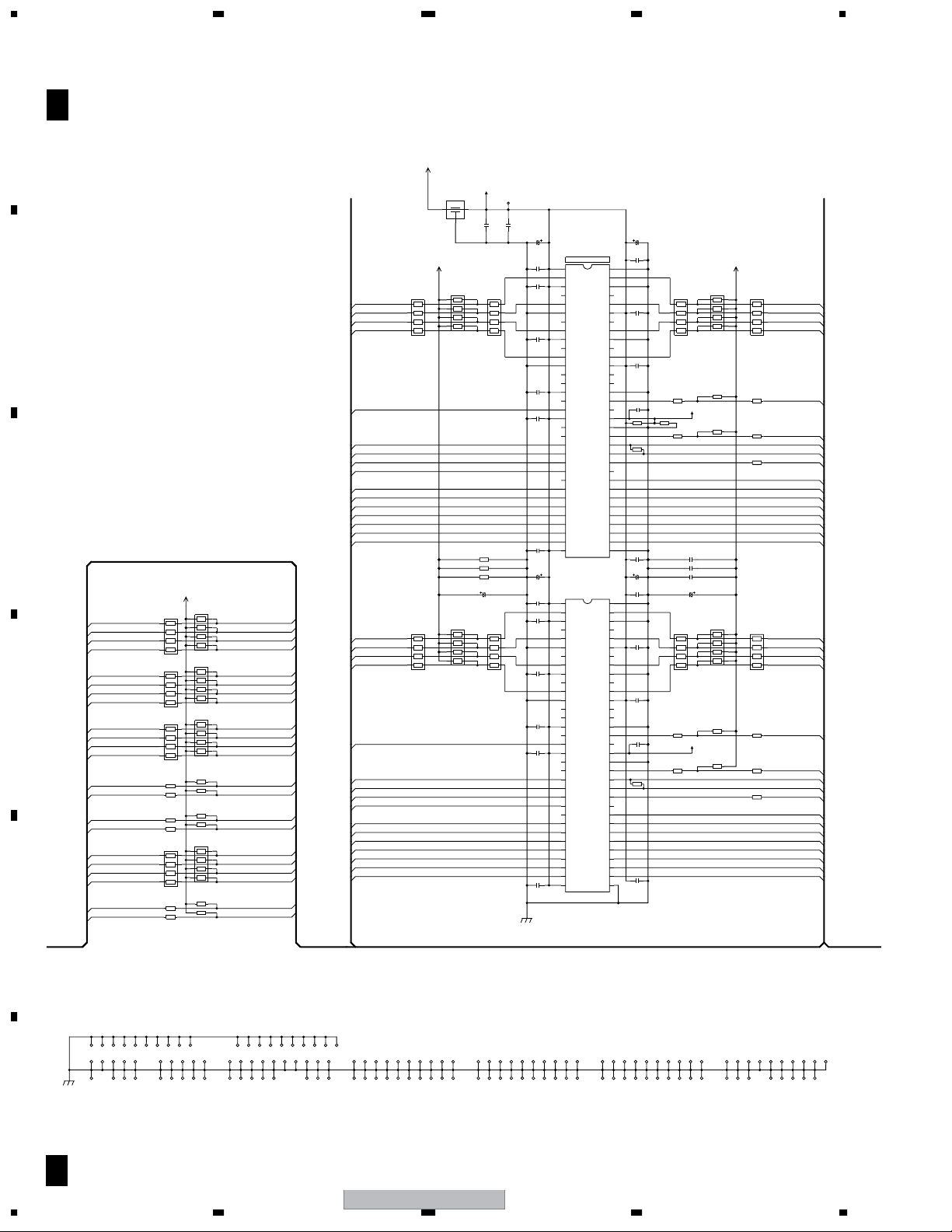
1234
3.5 MAIN ASSY 2/7
A
B
C
D
E
A 2/7
DRAM0_A12
DRAM0_A11
DRAM0_A9
DRAM0_A8
DRAM0_A13
DRAM0_A10
DRAM0_A0
DRAM0_A1
DRAM0_A7
DRAM0_A6
DRAM0_A5
DRAM0_A4
DRAM0_A3
DRAM0_BA0
DRAM0_BA1
DRAM0_WE
DRAM0_CAS
DRAM0_RAS
DRAM0_CS
DRAM0_CLK
DRAM0_CLKN
MAIN ASSY(VWV2234)
DRAM0_D0 DRAM0_D7
DRAM0_D1
DRAM0_D2
DRAM0_D3
DRAM0_TA13
DRAM0_TWE
DRAM0_TCAS
DRAM0_TRAS
DRAM0_TCS
DRAM0_TBA0 DRAM0_TA11
DRAM0_TBA1
DRAM0_TA10
DRAM0_TA0
DRAM0_TA1
DRAM0_TA2
DRAM0_TA3
VTT-A
R2091
R2081
NM
0R0
R2092
R2082
NM
0R0
R2093
R2083
NM
0R0
R2094
NM
R2084
0R0
R2079
R2078
NM
0R0
R2095
NM
R2085
0R0
R2096
R2086
NM
0R0
R2097
R2087
NM
0R0
R2098
NM
R2088
0R0
R2099
R2089
NM
0R0
DRAM0_TA12
DRAM0_TA11
DRAM0_TA9
DRAM0_TA8
DRAM0_TA13
DRAM0_TA10
DRAM0_TA0
DRAM0_TA1
DRAM0_TA7
DRAM0_TA6
DRAM0_TA5
DRAM0_TA4
DRAM0_TA3
DRAM0_TA2DRAM0_A2
DRAM0_TBA0
DRAM0_TBA1
DRAM0_TWE
DRAM0_TCAS
DRAM0_TRAS
DRAM0_TCS
DRAM0_TCLK
DRAM0_TCLKN
DRAM0_D8 DRAM0_D15
DRAM0_D9
DRAM0_D10
DRAM0_D11
DRAM0_TA13
DRAM0_TWE
DRAM0_TCAS
DRAM0_TRAS
DRAM0_TCS
DRAM0_TBA0
DRAM0_TBA1
DRAM0_TA10
DRAM0_TA0
DRAM0_TA1
DRAM0_TA2
DRAM0_TA3
V+2R6D-A
VTT-A
R2041
100
R2061
100
V+DDR-A
L2001
DTL1106-A
1
3
2
R2001
DDR0_TDATA0 DDR0_TDATA7
DDR0_TDATA1
DDR0_TDATA2
DDR0_TDATA3
NM
R2381
R2382
R2383
C2031
R2021
DDR0_TDATA8
DDR0_TDATA9
DDR0_TDATA10
DDR0_TDATA11
NM
104
105
C2012
C2001
C2035
IC2001
221/4
K4H510838C-UCCC
Clock:200MHz
C2002
1
VDD1
2
DQ0
3
VDDQ1
4
NC1
5
DQ1
6
VSSQ1
7
NC2
8
DQ2
9
VDDQ2
10
NC3
11
DQ3
12
VSSQ2
13
NC4
14
NC5
15
VDDQ3
16
NC6
17
NC7
18
VDD2
19
NC8
20
NC9
21
/WE
22
/CAS
23
/RAS
24
/CS
25
NC10
26
BA0
27
BA1
28
AP/A10
29
A0
30
A1
31
A2
32
A3
33
VDD334VSS1
K4H510838C-UCCC
1
VDD1
2
DQ0
3
VDDQ1
4
NC1
5
DQ1
6
VSSQ1
7
NC2
8
DQ2
9
VDDQ2
10
NC3
11
DQ3
12
VSSQ2
13
NC4
14
NC5
15
VDDQ3
16
NC6
17
NC7
18
VDD2
19
NC8
20
NC9
21
/WE
22
/CAS
23
/RAS
24
/CS
25
NC10
26
BA0
27
BA1
28
AP/A10
29
A0
30
A1
31
A2
32
A3
33
VDD334VSS1
IC2021
VSSQ5
VDDQ5
VSSQ4
VDDQ4
VSSQ3
VSSQ5
VDDQ5
VSSQ4
VDDQ4
VSSQ3
VSS3
DQ7
NC17
DQ6
NC16
DQ5
NC15
DQ4
NC14
NC13
DQS
NC12
VREF
VSS2
DM
/CK
CK
CKE
NC11
A12
A11
A9
A8
A7
A6
A5
A4
VSS3
DQ7
NC17
DQ6
NC16
DQ5
NC15
DQ4
NC14
NC13
DQS
NC12
VREF
VSS2
DM
/CK
CK
CKE
NC11
A12
A11
A9
A8
A7
A6
A5
A4
105
DDR0_DQ0
C2003
R2045
R2065
104
DDR0_DQ1 DDR0_DQ6
DDR0_DQ2
C2006
220
103
DDR0_DQ3
C2007
VCG1063-A
C2008
105
C2009
VCG1063-A
0R0
0R0
C2016
0R0
221/4
NM
C2021
105
DDR0_DQ8
C2022
104
DDR0_DQ9
DDR0_DQ10
C2025
220
103
DDR0_DQ11
C2026
VCG1063-A
C2027
105
C2028
VCG1063-A
C2015
VCH1234-A
C2004
105
66
65
64
63
62
C2005
61
103
60
59
58
57
56
C2010
55
VCG1063-A
54
53
52
51
C2013
50
49
104
48
R2005
47
1001
46
45
R2059
44
NM
43
42
41
40
39
38
37
36
35
C2011
104
C2036
221/4
C2023
105
66
65
DDR0_DQ15
64
63
62
C2024
61
103
60
59
DDR0_DQ13
58
57
56
DDR0_DQ12
C2029
55
VCG1063-A
54
53
52
51
DDR0_DQS1
C2014
50
49
104
48
47
46
45
R2077
44
NM
43
42
41
40
39
38
37
36
35
C2030
104
GND
DDR0_DQ7
DDR0_DQ5
DDR0_DQ4
DDR0_DQS0
R2006
1001
DDR0_DM0
DDR0_DQ14
DDR0_DM1
VTT-A
R2003
R2055
DDR0_TDATA6
DDR0_TDATA5
DDR0_TDATA4
220
DDR0_TDQS0
R2057
220
VREFD-A
DDR0_TDM0
R2058
220
NM
C2091
NM
C2092
NM
C2093
C2032
R2073
DDR0_TDATA15
DDR0_TDATA14
DDR0_TDATA13
DDR0_TDATA12
220
DDR0_TDQS1
R2075
220
VREFD-A
DDR0_TDM1
R2076
220
R2048
DRAM0_D6
DRAM0_D5
R2050
R2051
R2052
R2068
R2070
R2071
R2072
100
100
100
100
100
100
100
100
DRAM0_D4
DRAM0_DQS0
DRAM0_DM0
DRAM0_TCLKN
DRAM0_TCLK
DRAM0_TCLKE
DRAM0_TA12
DRAM0_TA9
DRAM0_TA8
DRAM0_TA7
DRAM0_TA6
DRAM0_TA5
DRAM0_TA4
DRAM0_D14
DRAM0_D13
DRAM0_D12
DRAM0_DQS1
DRAM0_DM1
DRAM0_TCLKN
DRAM0_TCLK
DRAM0_TCLKE
DRAM0_TA12
DRAM0_TA11
DRAM0_TA9
DRAM0_TA8
DRAM0_TA7
DRAM0_TA6
DRAM0_TA5
DRAM0_TA4
NM
R2010
NM
R2011
NM
NM
R2023
NM
R2030
NM
R2031
NM
F
GND
A 2/7
22
1234
BDP-HD1
Page 23
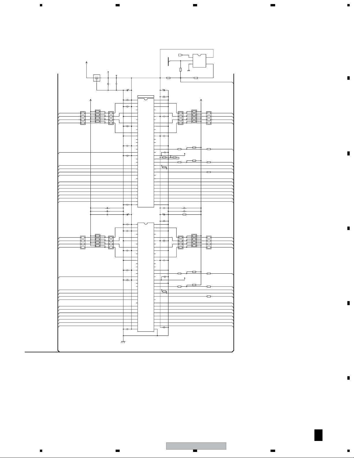
5 678
A
DRAM0_D16
DRAM0_D17
DRAM0_D18
DRAM0_D19
DRAM0_TA13
DRAM0_TWE
DRAM0_TCAS
DRAM0_TRAS
DRAM0_TCS
DRAM0_TBA0
DRAM0_TBA1
DRAM0_TA10
DRAM0_TA0
DRAM0_TA1
DRAM0_TA2
DRAM0_TA3
DRAM0_D24
DRAM0_D25
DRAM0_D26
DRAM0_D27
DRAM0_TA13
DRAM0_TWE
DRAM0_TCAS
DRAM0_TRAS
DRAM0_TCS
DRAM0_TBA0
DRAM0_TBA1
DRAM0_TA10
DRAM0_TA0
DRAM0_TA1
DRAM0_TA2
DRAM0_TA3
V+2R6D-C
VTT-A
R2941
100
R2961
100
DTL1106-A
3
RESET2#
DRAM0_CLKE
V+DDR-C
L2901
1
2
105
104
C2901
C2912
C2935
221/4
IC2901
K4H510838C-UCCC
Clock:200MHz
C2902
1
VDD1
105
C2903
104
C2906
103
C2907
VCG1063-A
C2908
105
C2909
VCG1063-A
C2916
221/4
C2921
105
C2922
104
C2925
103
C2926
VCG1063-A
C2927
105
C2928
VCG1063-A
2
DQ0
3
VDDQ1
4
NC1
5
DQ1
6
VSSQ1
7
NC2
8
DQ2
9
VDDQ2
10
NC3
11
DQ3
12
VSSQ2
13
NC4
14
NC5
15
VDDQ3
16
NC6
17
NC7
18
VDD2
19
NC8
20
NC9
21
/WE
22
/CAS
23
/RAS
24
/CS
25
NC10
26
BA0
27
BA1
28
AP/A10
29
A0
30
A1
31
A2
32
A3
33
VDD334VSS1
K4H510838C-UCCC
1
VDD1
2
DQ0
3
VDDQ1
4
NC1
5
DQ1
6
VSSQ1
7
NC2
8
DQ2
9
VDDQ2
10
NC3
11
DQ3
12
VSSQ2
13
NC4
14
NC5
15
VDDQ3
16
NC6
17
NC7
18
VDD2
19
NC8
20
NC9
21
/WE
22
/CAS
23
/RAS
24
/CS
25
NC10
26
BA0
27
BA1
28
AP/A10
29
A0
30
A1
31
A2
32
A3
33
VDD334VSS1
VSSQ5
VDDQ5
VSSQ4
VDDQ4
VSSQ3
IC2921
VSSQ5
VDDQ5
VSSQ4
VDDQ4
VSSQ3
DDR0_DQ16
R2901
R2945
DDR0_TDATA16
DDR0_DQ17
DDR0_TDATA17
DDR0_TDATA18
DDR0_TDATA19
C2981
C2982
C2983
DDR0_TDATA24
DDR0_TDATA25
DDR0_TDATA26
DDR0_TDATA27
DDR0_DQ18
220
DDR0_DQ19
NM
NM
NM
DDR0_DQ24
R2965
DDR0_DQ25
DDR0_DQ26
220
DDR0_DQ27
NM
R2921
NM
R2017
NM
C2915
VCH1234-A
C2904
105
66
VSS3
65
DQ7
NC17
DQ6
NC16
DQ5
NC15
DQ4
NC14
NC13
DQS
NC12
VREF
VSS2
DM
/CK
CK
CKE
NC11
A12
A11
A9
A8
A7
A6
A5
A4
VSS3
DQ7
NC17
DQ6
NC16
DQ5
NC15
DQ4
NC14
NC13
DQS
NC12
VREF
VSS2
DM
/CK
CK
CKE
NC11
A12
A11
A9
A8
A7
A6
A5
A4
DDR0_DQ23
64
63
62
61
60
59
58
57
56
55
VCG1063-A
54
53
52
51
50
49
48
47
46
45
44
43
42
41
40
39
38
37
36
35
66
65
64
63
62
61
60
59
58
57
56
55
VCG1063-A
54
53
52
51
50
49
48
47
46
45
44
43
42
41
40
39
38
37
36
35
R2955
DDR0_DQ22
C2905
103
DDR0_DQ21
DDR0_DQ20
C2910
R2957
DDR0_DQS2
C2913
220
R2906
104
1001
R2905
R2958
1001
DDR0_DM2
220
R2959
NM
C2911
C2991
C2992
104
C2936
R2393
221/4
C2923
105
DDR0_DQ31
R2973
DDR0_DQ30
C2924
103
DDR0_DQ29
DDR0_DQ28
C2929
R2975
DDR0_DQS3
C2914
220
104
R2976
DDR0_DM3
220
R2977
NM
C2930
104
IC2011
5
1
VCC
INB
2
INA
4
GND3OUTY
NM
0R0
R2019
GND
R2016
NM
DRAM0_TCLKE
VTT-A
R2903
DDR0_TDATA23
DDR0_TDATA22
DDR0_TDATA21
DDR0_TDATA20
220
DDR0_TDQS2
VREFD-A
DDR0_TDM2
NM
NM
0R0
DDR0_TDATA31
DDR0_TDATA30
DDR0_TDATA29
DDR0_TDATA28
220
DDR0_TDQS3
VREFD-A
DDR0_TDM3
R2948
DRAM0_D23
DRAM0_D22
DRAM0_D21
100
R2950
100
R2951
100
R2952
100
R2968
100
R2970
100
R2971
100
R2972
100
DRAM0_D20
DRAM0_DQS2
DRAM0_DM2
DRAM0_TCLKN
DRAM0_TCLK
DRAM0_TCLKE
DRAM0_TA12
DRAM0_TA11
DRAM0_TA9
DRAM0_TA8
DRAM0_TA7
DRAM0_TA6
DRAM0_TA5
DRAM0_TA4
DRAM0_D31
DRAM0_D30
DRAM0_D29
DRAM0_D28
DRAM0_DQS3
DRAM0_DM3
DRAM0_TCLKN
DRAM0_TCLK
DRAM0_TCLKE
DRAM0_TA12
DRAM0_TA11
DRAM0_TA9
DRAM0_TA8
DRAM0_TA7
DRAM0_TA6
DRAM0_TA5
DRAM0_TA4
NM
R2910
NM
R2911
NM
R2923
NM
R2930
NM
R2931
NM
B
C
D
GND
BDP-HD1
56
E
F
A 2/7
7
8
23
Page 24
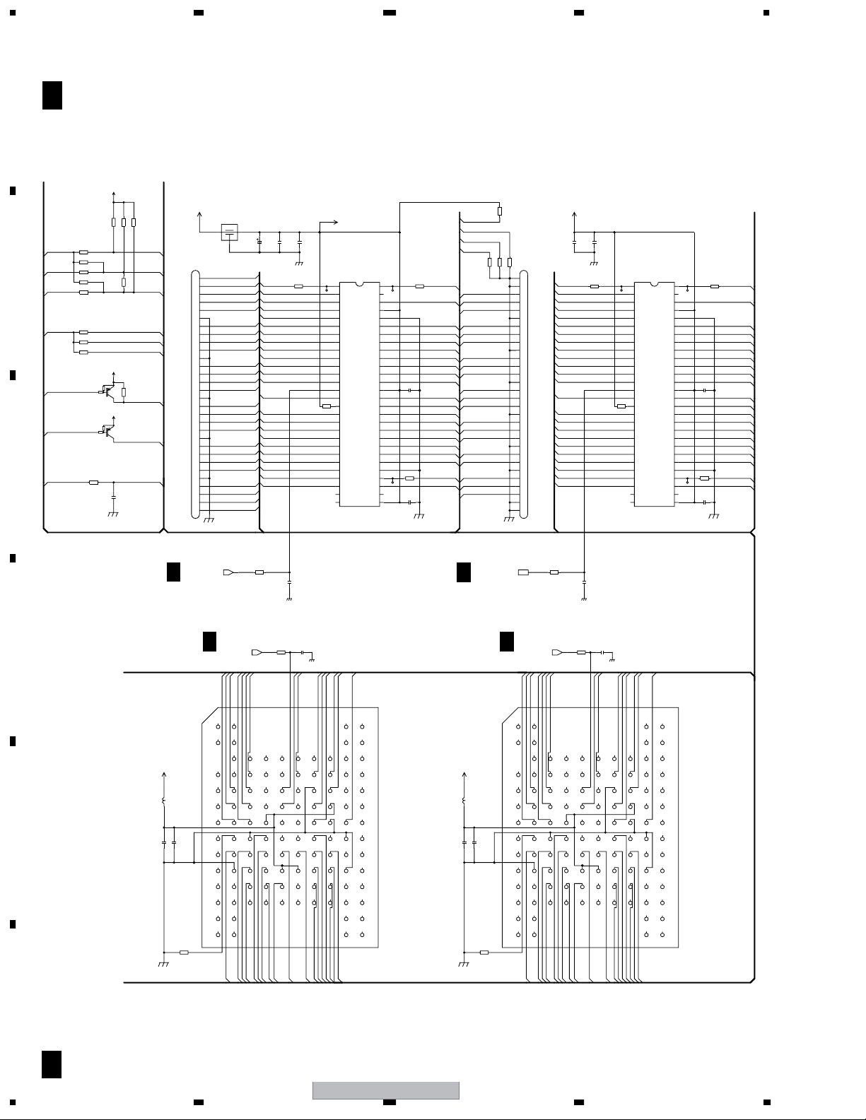
1234
3.6 MAIN ASSY 3/7
A
A 3/7
PB_CS2# FL_CS2#
PB_CS3#
B
PB_CS1#
PB_IORDY FL_RDY
DOC_INT3#
DOC_INT1#
C
PB_RD#
MAIN ASSY(VWV2234)
V+3FM
V+3D
L2701
DTL1106-A
1
CN2701
NM
30
29
28
27
26
25
24
23
22
21
20
19
18
17
16
15
14
13
12
11
10
9
8
7
6
5
4
3
2
1
3
2
GND
PB_A24
PB_A23
PB_A22
PB_A15
PB_A14
PB_A13
PB_A12
PB_A11
PB_A10
PB_A9
PB_A8
PB_A19
PB_A20
PB_WR#
PB_A21
PB_IORDY
PB_A18
PB_A17
PB_A7
PB_A6
PB_A5
PB_A4
PB_A3
PB_A2
PB_A1
C2706
221/4
PB_A22
PB_A15
PB_A14
PB_A13
PB_A12
PB_A11
PB_A10
PB_A9
PB_A8
PB_A19
PB_A20
PB_WR#
PB_A21
FL_RDY
PB_A18
PB_A17
PB_A7
PB_A6
PB_A5
PB_A4
PB_A3
PB_A2
PB_A1
C2702
106
GND
R2716
0R0
R2703
Q2792
Q2791
R2799
R2781
R2782
R2783
R2784
R2785
R2791
R2792
R2793
NM
103
R2786
R2788NMR2787
0R0
NM
NM
NM
NM
0R0
NM
NM
R2789
NM
DOC_RDY3
DOC_RDY1
DOC_CS3#
DOC_CS1#
V+3FM
NM
103
R2794
PB_INT
V+3FM
NM
PB_INT
C2799
PB_RD2#
NM
0R0
GND
C2701
104
0R0
V+3FM
IC2701
VYW2378
(S29GL512N10TFI020-K)
1
A23
2
A22
3
A15
4
A14
BYTE#
5
A13
VSS2
6
A12
DQ15/A-1
7
A11
8
A10
DQ14
9
A9
10
DQ13
A8
11
A19
12
DQ12
A20
13
WE#
14
RESET#
15
DQ11
A21
16
WP#/ACC
17
DQ10
RY/BY#
18
A18
19
A17
20
A7
21
A6
22
A5
23
A4
24
VSS1
A3
25
A2
26
A1
27
NC1
28
NC229VIO
CN2702
NM
9
8
7
6
5
4
3
2
1
V+3FM
C2762NMC2761
PB_A22
PB_A15
PB_A14
PB_A13
PB_A12
PB_A11
PB_A9
PB_A8
PB_A19
PB_A20
PB_WR#
PB_A21
FL_RDY
PB_A18
PB_A17
PB_A7
PB_A6
PB_A5
PB_A4
PB_A3
PB_A2
PB_A1
R2768
GND
NM
IC2761
NM
1
A23
2
3
4
5
6
7
8
9
10
11
12
13
14
15
16
17
18
19
20
21
22
23
24
25
26
27
28
A22
A15
A14
BYTE#
A13
A12
DQ15/A-1
A11
A10
A9
A8
A19
A20
WE#
RESET#
A21
WP#/ACC
RY/BY#
A18
A17
A7
A6
A5
A4
A3
A2
A1
NC1
NC229VIO
VSS2
DQ14
DQ13
DQ12
DQ11
DQ10
VSS1
NC5
NC4
A16
DQ7
DQ6
DQ5
DQ4
VCC
DQ3
DQ2
DQ9
DQ1
DQ8
DQ0
OE#
CE#
NC3
NM
R2763
NM
R2767
56
55
54
53
52
51
50
49
48
47
46
45
44
43
42
41
40
39
38
37
36
35
34
33
32
31
A0
30
C2763
R2769
C2764
PB_A24PB_A24 PB_A23PB_A23
NM
PB_A16
PB_AD15
PB_AD7
PB_AD14PB_A10
PB_AD6
PB_AD13
PB_AD5
PB_AD12
PB_AD4
NM
PB_AD11
PB_AD3
PB_AD10
PB_AD2
PB_AD9
PB_AD1
PB_AD8
PB_AD0
PB_RD2#
DOC_CS1#
NM
PB_A0
NM
GND
103
R2711
PB_IORDY
PB_AD7
PB_DMARQ
PB_INT
103
103
103
R2712
R2713
R2714
GND
30
29
28
27
26
25
24
23
22
21
20
19
18
17
16
15
14
13
12
11
10
NC4
A24
A16
DQ7
DQ6
DQ5
DQ4
VCC
DQ3
DQ2
DQ9
DQ1
DQ8
DQ0
OE#
CE#
A0
NC3
0R0
55
54
53
52
51
50
49
48
47
46
45
44
C2703
43
42
105
41
40
39
38
37
36
35
34
33
32
R2717
0R0
31
30
C2704
105
PB_A16
PB_AD15
PB_AD7
PB_AD14
PB_AD6
PB_AD13
PB_AD5
PB_AD12
PB_AD4
PB_AD11
PB_AD3
PB_AD10
PB_AD2
PB_AD9
PB_AD1
PB_AD8
PB_AD0
PB_RD2#
FL_CS2#
PB_A0
GND
PB_A16
PB_AD15
PB_AD7
PB_AD14
PB_AD6
PB_AD13
PB_AD5
PB_AD12
PB_AD4
PB_AD11
PB_AD3
PB_AD10
PB_AD2
PB_AD9
PB_AD1
PB_AD8
PB_AD0
PB_RD#
PB_CS0#
PB_A0
R2715
56
RESET2#
R2706
A 1/7
0R0
102
C2705
A 1/7
GND
D
NM
L2721
E
C2722
NM
NM
C2721
R2727
NM
RESET2# RESET2#
PB_A7
PB_A1
PB_A2
PB_A3
PB_A4
PB_A5
PB_A6
A1
NC_A1A2NC_A2
B1
NC_B1B2NC_B2
C2
NC_C2C3NC_C3C4NC_C4C5NC_C5C6NC_C6C7NC_C7C8NC_C8C9NC_C9
D1
D3A7D4
NC_D1D2NC_D2
E1
E2A3E3A6E4
NC_E1
F1
F2A2F3A5F4
NC_F1
G1
G2A1G3A4G4
NC_G1
H1
H2A0H3
NC_H1
VSS_H3
J1
J2
CE#J3OE#
NC_J1
K1
K2
K3D0K4
NC_K1
RSRVD_K2
L1
L3D8L4D2L5
NC_L1L2NC_L2
M1
NC_M1M2NC_M2M3NC_M3M4NC_M4M5NC_M5M6NC_M6M7NC_M7M8NC_M8M9NC_M9
N1
NC_N1N2NC_N2
P1
NC_P1P2NC_P2
PB_RD2#
DOC_CS3#
PB_AD8
PB_AD0
R2726
NM
RSRVD_D4D5RSRVD_D5
RSTIN#
RSRVD_E4
NC_F4F5BUSY#
NC_G5G6NC_G6
IF_CFG
H4D1H5
NC_H5H6NC_H6
J4D9J5D3J6D4J7
D10K5VCC
D11
PB_AD9
PB_AD10
PB_AD11
PB_AD2
PB_AD1
E5
G5
C2725
NM
PB_WR#
DOC_RDY3
WE#
RSRVD_E6E7RSRVD_E7
RSRVD_F6
VCCQ
RSRVD_L6
PB_AD3
GND
PB_A8
PB_A9
PB_A12
PB_A10
PB_A11
DOC_INT3#
A9
A10
NC_A9
NC_A10
B9
B10
NC_B9
NC_B10
C10
PB_AD13
PB_AD12
A11
E8
A12
LOCK#
RSRVD_H8
K8D7K9
D14
PB_AD14
PB_AD6
PB_AD15
PB_AD7
NC_D9
RSRVD_E9
RSRVD_F9
IRQ#
ID1
RSRVD_J9
VSS_K9
NC_L9
NC_N9
NC_P9
NC_C10
D9
D10
NC_D10
E9
E10
NC_E10
F9
F10
NC_F10
G9
G10
NC_G10
H9
J9
L9
N9
P9
NM
H10
NC_H10
IC2721
J10
NC_J10
K10
NC_K10
L10
NC_L10
M10
NC_M10
N10
NC_N10
P10
NC_P10
D6
D7A8D8
E6
F6
F7A9F8
G7
A10G8ID0
H7D6H8
D13J8D15
K6
K7
D12
L6
L7D5L8
PB_AD4
PB_AD5
V+3FMV+3FM
L2741
C2742NMC2741
GNDGND
RESET2#
R2766
NM
NM
C2765
GND
A 1/7A 1/7
PB_A6
PB_A5
PB_A2
PB_A1
PB_A4
PB_A3
PB_A7
A1
NC_A1A2NC_A2
B1
NC_B1B2NC_B2
C2
NC_C2C3NC_C3C4NC_C4C5NC_C5C6NC_C6C7NC_C7C8NC_C8C9NC_C9
D1
D3A7D4
NC_D1D2NC_D2
E1
E2A3E3A6E4
NM
NC_E1
F1
F2A2F3A5F4
NC_F1
G1
G2A1G3A4G4
NC_G1
H1
H2A0H3
NC_H1
VSS_H3
J1
J2
CE#J3OE#
NC_J1
K1
K2
K3D0K4
NC_K1
RSRVD_K2
L1
L3D8L4D2L5
NC_L1L2NC_L2
M1
NC_M1M2NC_M2M3NC_M3M4NC_M4M5NC_M5M6NC_M6M7NC_M7M8NC_M8M9NC_M9
N1
NC_N1N2NC_N2
P1
NC_P1P2NC_P2
DOC_CS1#
PB_AD8
PB_RD2#
PB_AD0
R2747
NM
NM
R2746
RSRVD_D4D5RSRVD_D5
RSRVD_E4
NC_F4F5BUSY#
IF_CFG
H4D1H5
J4D9J5D3J6D4J7
D10K5VCC
PB_AD2
PB_AD11
PB_AD10
PB_AD1
PB_AD9
NM
E5
RSTIN#
G5
NC_G5G6NC_G6
NC_H5H6NC_H6
D11
PB_AD3
C2745
NM
GND
PB_WR#
DOC_RDY1
D6
WE#
E6
RSRVD_E6E7RSRVD_E7
F6
RSRVD_F6
K6
VCCQ
L6
RSRVD_L6
PB_AD4
PB_A8
D7A8D8
F7A9F8
G7
A10G8ID0
H7D6H8
D13J8D15
K7
D12
L7D5L8
PB_AD12
PB_AD5
PB_A9
PB_A10
A11
A12
LOCK#
RSRVD_H8
D14
PB_AD6
PB_AD14
PB_AD13
PB_A11
PB_A12
E8
K8D7K9
PB_AD7
PB_AD15
NC_A9
NC_B9
NC_D9
RSRVD_E9
RSRVD_F9
IRQ#
ID1
RSRVD_J9
VSS_K9
NC_L9
NC_N9
NC_P9
A9
B9
D9
E9
F9
G9
H9
J9
L9
N9
P9
DOC_INT1#
A10
NC_A10
B10
NC_B10
C10
NC_C10
D10
NC_D10
E10
NC_E10
F10
NC_F10
G10
NC_G10
H10
NC_H10
J10
NC_J10
K10
NC_K10
L10
NC_L10
M10
NC_M10
N10
NC_N10
P10
NC_P10
NM
IC2741
F
A 3/7
24
1234
BDP-HD1
Page 25
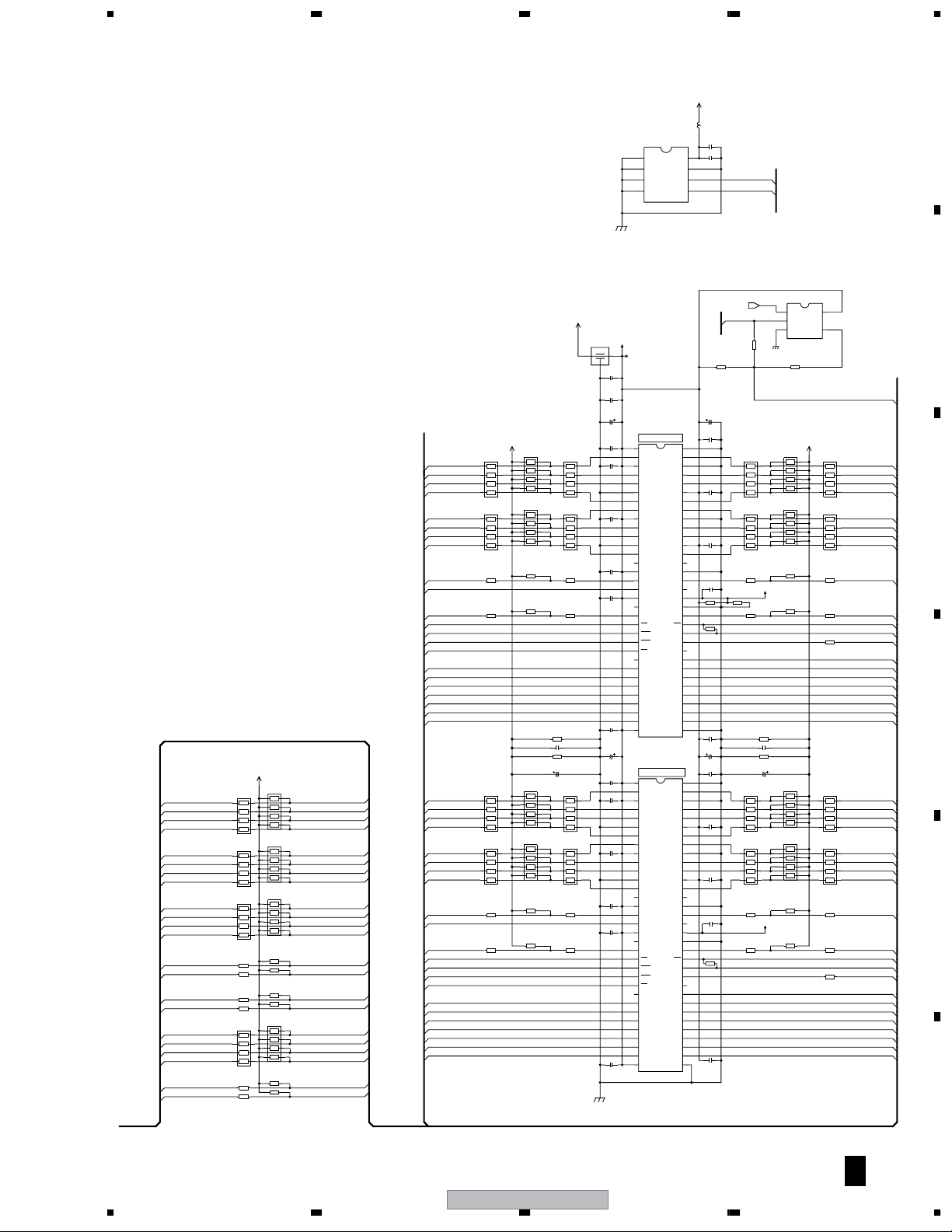
5 678
DRAM1_A12
DRAM1_A11
DRAM1_A9
DRAM1_A8
DRAM1_A13
DRAM1_A10
DRAM1_A0
DRAM1_A1
DRAM1_A7
DRAM1_A6
DRAM1_A5
DRAM1_A4
DRAM1_A3
DRAM1_A2
DRAM1_BA0
DRAM1_BA1
DRAM1_WE
DRAM1_CAS
DRAM1_RAS
DRAM1_CS
DRAM1_CLK
DRAM1_CLKN
R2181
R2182
R2183
R2184
R2178
R2185
R2186
R2187
R2188
R2189
100
100
100
100
100
100
100
100
100
100
VTT-B
R2191
R2192
R2193
R2194
R2195
R2196
R2197
R2198
R2199
R2179
V+3D
L2801
C2801
CTF1394-A
IC2801
1
A0
2
A1
3
A2
45
GND
106
8
C2802
Vcc
104
7
WP
6
SCL
SDA
I2C_SCL
I2C_SDA
A
BR24L01AFJ-W
GND
R2119
0R0
GND
VREFD-B
0R0
NM
0R0
NM
VREFD-B
1
INB
2
INA
GND3OUTY
R2116
NM
R2103
NM
R2107
NM
R2110
NM
R2111
NM
R2123
NM
R2127
NM
R2130
NM
R2131
NM
IC2111
5
VCC
4
NM
B
DRAM1_TCLKE
R2148
DRAM1_D15
DRAM1_D14
DRAM1_D13
DRAM1_D12
100
R2149
R2150
R2151
R2152
R2168
R2169
R2170
R2171
R2172
100
100
100
100
100
100
100
100
100
DRAM1_D11
DRAM1_D10
DRAM1_D9
DRAM1_D8
DRAM1_DQS1
DRAM1_DM1
DRAM1_TCLKN
DRAM1_TCLK
DRAM1_TCLKE
DRAM1_TA12
DRAM1_TA11
DRAM1_TA9
DRAM1_TA8
DRAM1_TA7
DRAM1_TA6
DRAM1_TA5
DRAM1_TA4
DRAM1_D31
DRAM1_D30
DRAM1_D29
DRAM1_D28
DRAM1_D27
DRAM1_D26
DRAM1_D25
DRAM1_D24
DRAM1_DQS3
DRAM1_DM3
DRAM1_TCLKN
DRAM1_TCLK
DRAM1_TCLKE
DRAM1_TA12
DRAM1_TA11
DRAM1_TA9
DRAM1_TA8
DRAM1_TA7
DRAM1_TA6
DRAM1_TA5
DRAM1_TA4
C
D
E
F
RESET2#
66
65
64
63
62
61
60
59
58
57
56
55
54
53
52
51
50
49
48
47
46
45
44
43
42
41
40
39
38
37
36
35
66
65
64
63
62
61
60
59
58
57
56
55
54
53
52
51
50
49
48
47
46
45
44
43
42
41
40
39
38
37
36
35
C2115
VCH1234-A
C2104
105
C2105
103
C2110
VCG1063-A
C2113
104
R2105
1001
R2159
NM
C2111
104
C2136
221/4
C2123
105
C2124
103
C2129
VCG1063-A
C2114
104
R2177
NM
C2130
104
DRAM1_CLKE
R2117
NM
R2106
R2155
220
R2156
220
R2157
220
1001
R2158
220
R2491
C2192
R2493
C2132
R2173
220
R2174
220
R2175
220
R2176
220
V+2R6D-B
L2101
DTL1106-A
V+DDR-B
1
3
2
C2101
105
C2112
104
C2135
IC2101
221/4
K4H511638C-UCCC-K
VTT-B VTT-B
R2101
DRAM1_D0
DRAM1_D1
DRAM1_D2
DRAM1_D3
DRAM1_D4
DRAM1_D5
DRAM1_D6
DRAM1_D7
DRAM1_DQS0
DRAM1_TA13
DRAM1_DM0
DRAM1_TWE
DRAM1_TCAS
DRAM1_TRAS
DRAM1_TCS
DRAM1_TBA0
DRAM1_TBA1
DRAM1_TA10
DRAM1_TA0
DRAM1_TA1
DRAM1_TA2
DRAM1_TA3
DRAM1_TA12
DRAM1_TA11
DRAM1_TA9
NM
NM
NM
NM
NM
NM
NM
NM
NM
NM
DRAM1_TA8
DRAM1_TA13
DRAM1_TA10
DRAM1_TA0
DRAM1_TA1
DRAM1_TA7
DRAM1_TA6
DRAM1_TA5
DRAM1_TA4
DRAM1_TA3
DRAM1_TA2
DRAM1_TBA0
DRAM1_TBA1
DRAM1_TWE
DRAM1_TCAS
DRAM1_TRAS
DRAM1_TCS
DRAM1_TCLK
DRAM1_TCLKN
DRAM1_D16
DRAM1_D17
DRAM1_D18
DRAM1_D19
DRAM1_D20
DRAM1_D21
DRAM1_D22
DRAM1_D23
DRAM1_DQS2
DRAM1_TA13
DRAM1_DM2
DRAM1_TWE
DRAM1_TCAS
DRAM1_TRAS
DRAM1_TCS
DRAM1_TBA0
DRAM1_TBA1
DRAM1_TA10
DRAM1_TA0
DRAM1_TA1
DRAM1_TA2
DRAM1_TA3
R2141
R2142
R2143
R2144
R2161
R2162
R2163
R2164
100
100
100
100
100
100
100
100
R2104
R2112
R2153
R2121
R2124
R2114
R2115
R2145
NM
220
R2146
NM
220
NM
R2147
220
NM
R2140
220
0R0
R2481
NM
C2182
0R0
R2483
NM
C2131
R2165
NM
220
R2166
NM
220
NM
R2167
220
NM
R2160
220
GND
C2102
105
C2103
104
C2106
103
C2107
VCG1063-A
C2108
105
C2109
VCG1063-A
C2116
221/4
C2121
105
C2122
104
C2125
103
C2126
VCG1063-A
C2127
105
C2128
VCG1063-A
Clock:200MHz
1
VDD1
VSS3
2
DQ0
DQ15
3
VDDQ1
VSSQ5
4
DQ1
DQ14
5
DQ2
DQ13
6
VSSQ1
VDDQ5
7
DQ3
DQ12
8
DQ4
DQ11
9
VDDQ2
VSSQ4
10
DQ5
DQ10
11
DQ6
12
VSSQ2
VDDQ4
13
DQ7
14
NC1
15
VDDQ3
VSSQ3
16
LDQS
UDQS
17
NC2
18
VDD2
VREF
19
NC3
VSS2
20
LDM
21
WE
22
CAS
23
RAS
24
CS
25
NC4
26
BA0
27
BA1
28
AP/A10
29
A0
30
A1
31
A2
32
A3
33
VDD334VSS1
IC2121
K4H511638C-UCCC-K
Clock:200MHz
1
VDD1
VSS3
2
DQ0
DQ15
3
VDDQ1
VSSQ5
4
DQ1
DQ14
5
DQ2
DQ13
6
VSSQ1
VDDQ5
7
DQ3
DQ12
8
DQ4
DQ11
9
VDDQ2
VSSQ4
10
DQ5
DQ10
11
DQ6
12
VSSQ2
VDDQ4
13
DQ7
14
NC1
15
VDDQ3
VSSQ3
16
LDQS
UDQS
17
NC2
18
VDD2
VREF
19
NC3
VSS2
20
LDM
21
WE
22
CAS
23
RAS
24
CS
25
NC4
26
BA0
27
BA1
28
AP/A10
29
A0
30
A1
31
A2
32
A3
33
VDD334VSS1
DQ9
DQ8
NC7
NC6
UDM
CK
CK
CKE
NC5
A12
A11
A9
A8
A7
A6
A5
A4
DQ9
DQ8
NC7
NC6
UDM
CK
CK
CKE
NC5
A12
A11
A9
A8
A7
A6
A5
A4
56
BDP-HD1
A 3/7
7
8
25
Page 26
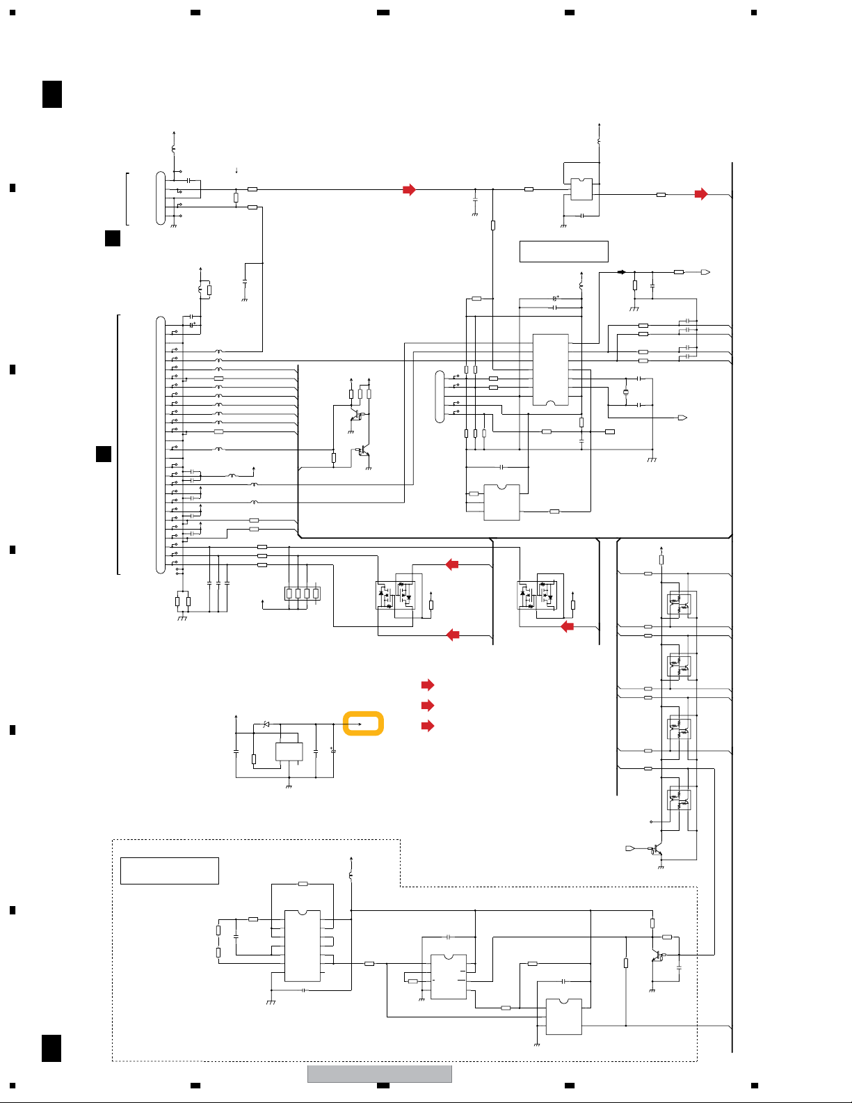
1234
3.7 MAIN ASSY 4/7
A
B
C
D
E
F
A 4/7
MAIN ASSY(VWV2234)
V+5E
L3401
CN3401
CN2001
SEL_CONT
SRJB
E
LED_FL OFF
LED_STAND BY
LED_Blue
CN101
LED_LAN
LED_HDMI
LED_Blue
LED_STAND BY
FLKY
LED_PON
B
RESET_OUT
LED_STAND BY
LED_STAND BY
Super LED
KM200TA5
V+5E
GND
R_CONT
GND
CN3501
52044-2845
GND
V+13E
GND
IR
KEY1
LED_HD
GND
GND
V+5E
KEY2
FLDC-
KEY3
FLDC+
FL-28V
FLDATA
FLCLK
FLSTB
CTF1394-A
C3401
5
106
4
3
2
1
The R3403 arrangement side B.
R3401
220
NM
R3402
R3403
220
GND
V+13E
101
C3402
NM
R3510
L3510
VTL1175-A
GND
C3501
104
R3501
C3506
NM
L3511
CTF1306
L3512
CTF1306
L3513
CTF1306
R3514
103
L3515
CTF1306
L3516
CTF1306
L3517
CTF1306
L3518
CTF1306
L3519
CTF1306
R3520
103
L3521
CTF1306
L3501
C3507
CTF1394-A
102
C3502
104
FLDC-
C3503
104
FLDC+
C3504
104
FL-28V
C3505
104
220
220
C6703
C6704
C6705
0R0
0R0
R3502
FrontLED1
LED2
FrontLED3
FrontLED4
FrontLED5
FrontLED6
FrontLED7
LED8
V+5E
L3523
CTF1306
L3524
CTF1306
R3525
103
R3526
103
R3527
R3528
R3529
220
V+5E
FrontLED9
LED10
LED11
220
220
220
658
7
102
R3503
214
3
1
2
3
4
5
6
7
8
9
10
11
12
13
14
15
16
17
18
19
20
21
22
23
24
25
26
27
28
GND
V+6E
D3801
NM
5
VOUT
225
R3801
R3763
101
104
ON/OFF
0R0
1234
TC74VHCU04FT
1
2
3
4
5
6
7
C3801
103
R3762
C3761
393
R3761
VSS
NC VIN
IC3801
S-1170B50UC-OUJ
GND
R3764
0R0
IC3751
1A
1Y
2A
2Y
3A
3Y
GND
C3751
105
106
C3802
14
VCC
13
6A
12
6Y
11
5A
10
5Y
9
4A
8
4Y
GND
C3803
V+3D
L3635
CTF1357
IC3631
TC7SH08FUS1
1
(SEL)
C3632
101
220
GND
R3634
104
NM
R3602
104
R3618
220
V+5E
V+3D
NM
NM
R3562NMR3564
R3561
Q3561
NM
GND
Q3562
NM
220
R3563
GND
5
6
Q3554
UM6K1N
1
2
V+5E
101/16
5
4
3
2
VKN1374-A
CN3601
1
V+3D V+3D
R3554
34
(SEL)
: SEL_CONT ROUTE
(FIP)
: FIP ROUTE
(ETH)
: ETH ROUTE
R3616
R3603
220
NM
R3605NMR3606
R3607
104
IC3641
1
R3642
0R0
NM
(FIP)
(FIP)
FIP_STB
FIP_CLK
ER
2
SUB
GND3VOUT
R3631
R3632
SubMicon
C3601
C3602
8
9
10
11
12
13
14
C3641
NM
NM
5
VDD
4
RESET IC
6
Q3553
UM6K1N
1
220
IC3601
PE0003D
(PIC16F688-I/SL)
AN6
AN5
AN4
INT
ICSPCLK
ICSPDAT
VSS
R3604
220
R3641
5
2
CLKOUT
NM
V+3D
L3701
CTF1357
C3701
105
IC3701
R3703
220
TC7WH74FU
1
CK
2
D
3
Q
R3702
45
0R0
GND
8
Vcc
7
PR
6
CLR
Q
GND
R3713
NM
R3711
220
TC7SH08FUS1
1
INB
2
INA
GND3OUTY
5
INB
VCC
2
INA
4
GND3OUTY
C3631
105
GND
V+5E
L3601
101/16
CTF1394-A
104
AN7
7
RC4
6
RC5
5
VPP
4
3
CLKIN
2
VDD
1
R3608
102
C3608
104
0R0
R3553
34
FIP_DATA
(FIP)
C3702
105
IC3711
5
VCC
4
GND
X3601
SUB_RESET#
R3633
R3617
R3612
R3613
R3614 102
R3615 102
C3603
NM
NM
C3604
LED1
LED3
LED4
LED5
LED6
LED7
LED9
RESET3#
NM
R3712
220
R3611
220
103
101
C3611
C3612
NM
NM
C3613
NM
NM
C3614
220
C3615
220
POWER_ON
MAIN LSI
W.Reset
I2C_SCL
I2C_SDA
I2CS_SCL
I2CS_SDA
IR
GND
V+3D
332
R3787
R3781
332
R3782
332
R3783
332
R3784
332
R3785
332
R3786
332
R3788
332
GND
103
R3721
R3722
Q3721
DTC124EUA
GND
Q3781
Q3782
Q3783
Q3785
Q3784
DTC124EUA
NM
FrontLED1
E2
C1
4
5B26
UMH9N
3
E11B12C2
FrontLED3
FrontLED4
E2
C1
4
5B26
UMH9N
3
E11B12C2
FrontLED5
FrontLED6
E2
C1
4
5B26
UMH9N
3
E11B12C2
FrontLED7
E2
C1
4
5B26
UMH9N
3
E11B12C2
NM
C3721
FrontLED9
A 4/7
26
GND
BDP-HD1
1234
Page 27
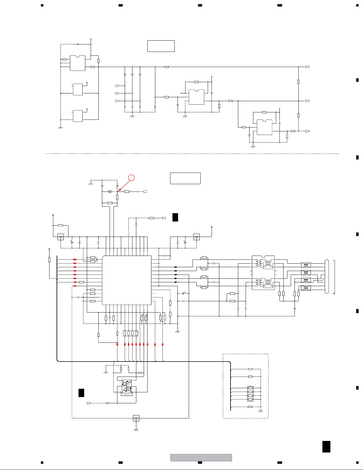
5 678
V+3D
R3903
V+3LH
103
R3055
ETH_MDINT#
104
GND
R3002
L3002
DTL1106-A
1
ETH_COL
NM
2
ETH_TXEN
ETH_TXD3
ETH_TXD2
ETH_TXD1
ETH_TXD0
ETH_TXC
VWV2249
3
IC3901
BD45282G
1
ER
2
SUB
GND3VOUT
IC3903
NC
3
GND
4
IC3902
BU4809F
NC
3
GND
4
R3002:0R0
C3004
C3111
C3901
221/4
V+3D
105
5
VDD
NM
VDD
2
VOUT
1
VDD
2
VOUT
1
223
R3902
R3901
4
0R0
V+2R6D
V+1R2D
F_RESET#
JTAG_RESET#
SUB_RESET#
D3901NMD3902
NM
C3902
C3903
D3903
RB520S-30
101
C3904
NM
NM
RESET
R3916
NM
R3911
101
101
C3905
C3911
102
GNDGND
R3912
IC3911
1
INB
2
INA
GND3OUTY
TC7SH08FUS1
RESET#
MAIN LSI
V+3D
105
R3923
0R0
R3914
DDR CLKE
RESET2#
NOR FLASH
NAND FLASH
ETHER
HDMI
NM
R3925
RESET3#
R3924
101
103
LED
LAN
MUTE
(during RESET)
101
5
VCC
105
C3912
R3913
R3915
101
103
1
R3921
2
0R0
102
TC7SH08FUS1
C3922
R3922
101
IC3921
INB
INA
GND3OUTY
V+3D
5
VCC
C3921
4
4
A
B
GND
2
200
GND
C3041
25MHz
R3054
R3014
R3015
R3016
103
R3056
103
103
103
102
C3006
1
COL
2
TXEN
3
NM
TXD3
4
TXD2
5
TXD1
6
TXD0
7
TXC
8
PWFBIN
9
LED0/PHYAD0
10
LED1/PHYAD1
11
DGND1
12
LED2/PHYAD2
NM
R3019
102
C3005
R1303
220
104
X3001
VSS1215-A
R3041
NM
48
47
131415
103
R3017
DVDD33_2
X2
105
C3007
R3018
13
14
15
103
R1306
150
C3042
R3043
NM
0R0
R3042
C3044
40
41
42
43
44
45X1464748
LDPS
ISOLATE
MII/SNIB/RTT3
IC3001
RESETB
3837DUPLEX
ANE
24 RXER/FXEN
RPTR
DGND3
RTL8201CP-LF
LED3/PHYAD3
DVDD33_1
LED4/PHYAD4
RXC16DGND217RXD318RXD219RXD120RXD021RXDV22CRS
R3053
658
7
220
R3011
214
3
220
CLK25M
102
SPEED
PWFBOUT
23
103
AVDD33
AGND2
TPTX+
TPTX-
TPRX+
TPRX-
AGND
RTSET
MDIO
R3044
373839
MDC
24
0R0
36
35
34
33
32
31
30
29
28
27
NC
26
25
103
R3052
RESET2#
102
R3051
C3003
102
R3057
R3012
R3013
NM
Ether
A 1/7
102
C3002
C3001
C3112
330/25
C3113
104
1001
1001
GND
221/4
L3001
DTL1106-A
3
C
V+3LH
1
2
T3001
R3021
C3021
R3022
R3023
C3022
R3024
49R9
49R9
49R9
49R9
BTX1044-A
1
2
104
104
R3211
0R0
R3212
0R0
3
4
5
6
7
89
104
104
C3202
C3203
16
15
14
13
12
11
10
75R0
R3202
R3201
75R0
VTH1056-A-T
1
23
VTH1056-A-T
1
23
VTH1056-A-T
1
23
1
23
VTH1056-A-T
75R0
R3203
R3204
C3201
ACG1127-A
75R0
CN3001
VKN2023-A
L3201
4
1
2
L3202
4
L3203
4
L3204
4
ETHERNET
3
4
5
6
7
8
D
LAN
ETH_RXD3
ETH_RXDV
ETH_RXD2
ETH_RXD1
A 1/7
RESET3#
GND
R3035
103
R3033
Q3031
UM6K1N
1
2
3D24
R3032
NM
ETH_RXD0
103
ETH_CRS
R3031
R3034
6
D1
5
G2
S2
L3101
DTL1106-A
3
2
ETH_RXC
ETH_RXERR
S1
G1
0R0
ETH_MDC
ETH_MDIO
NM
1
GND
BDP-HD1
56
ETH_TXC
ETH_RXC
ETH_RXD0
ETH_RXD1
ETH_RXD2
ETH_RXD3
ETH_RXDV
E
R3251
NM
R3252
NM
R3253
NM
8
1
7
2
6
3
5
4
R3254
NM
GND
F
A 4/7
7
8
27
Page 28
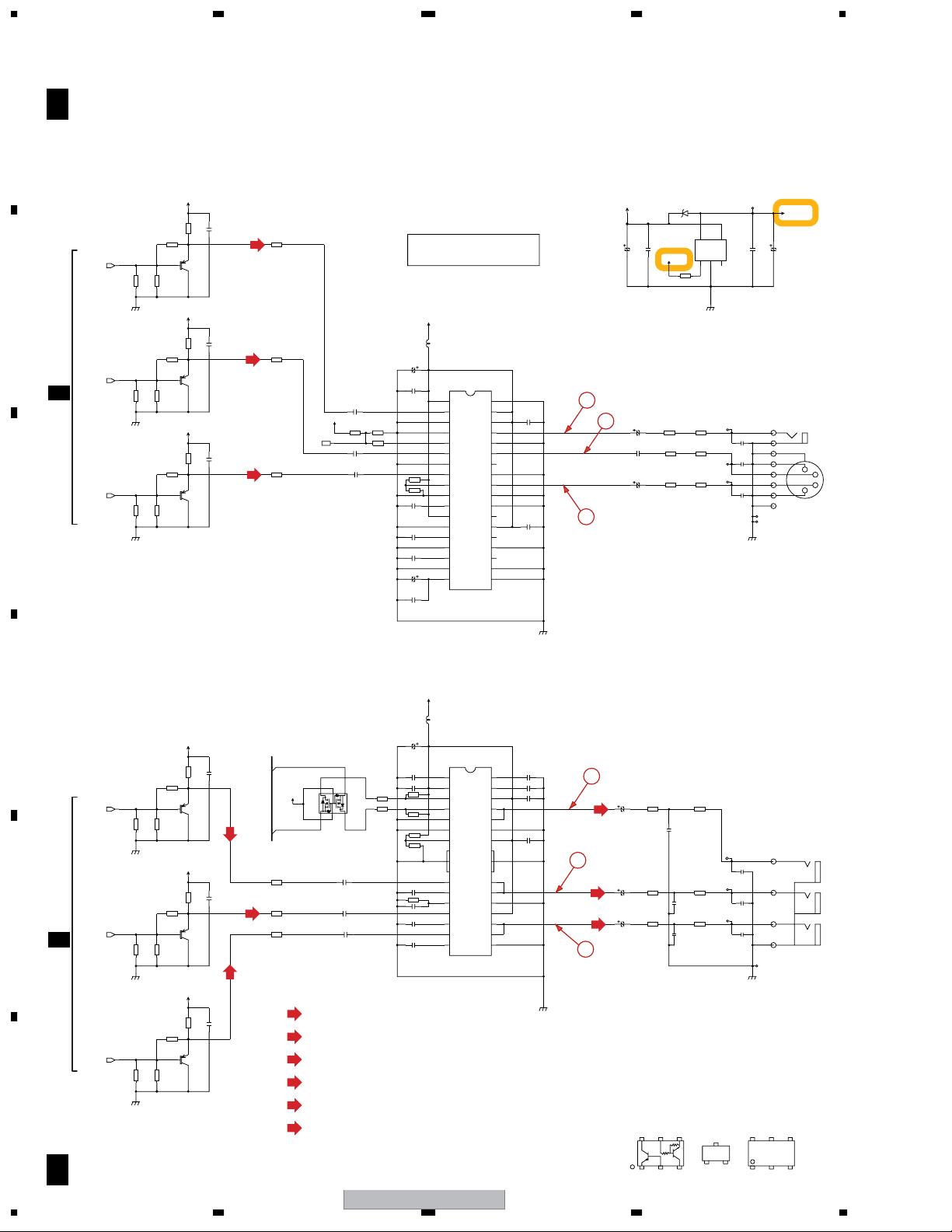
1234
3.8 MAIN ASSY 5/7
A
B
C
A 5/7
CVBS
SVid-C
A 1/7A 1/7
SVid-Y
MAIN ASSY(VWV2234)
V+5V
681
105
(CV_BS)
R4123
GND
GND
GND
R4121
R4131
R4141
R4125
NM
75R0
75R0
R4122
R4135
NM
75R0
75R0
R4132
R4145
NM
75R0
75R0
R4142
V+5V
V+5V
R4133
R4143
C4121
Q4121
2SA1576A(QR)
681
C4131
Q4131
2SA1576A(QR)
681
C4141
Q4141
2SA1576A(QR)
105
(SV_C)
105
(SV_Y)
R4124
R4134
R4144
0R0
0R0
C4151
106
V+3S
R4191
103
V_MUTE
C4152
106
C4153
0R0
106
R4193
VIDEO AMP
V+5V
L4101
C4101
101/16
C4102
104
R4192
NM
0R0
R4118
NM
R4119
0R0
C4104
104
C4105
104
C4106
104
C4107
470/16
C4108
104
CTF1394-A
IC4101
LA73054
1
VCC1
AMP-1.SW
2
0COMPOSITE.IN
DRIVE-1.SW
3
SQUEEZE.SW
VCC21
4
LETTER-BOX.SW
COMPOSITE.OUT
5
MUTE-1.SW
GND21
6
CHROMA.IN
CHROMA.OUT
7
GND11
C_DC.OUT
8
Y-1.IN
GND22
9
YC-MIX.SW
Y-1.OUT
10
RGB.SW
GND23
11
Y-2.IN
GND24
12
MUTE-2.SW
Y-2.OUT
13
LPF.SW
VCC22
14
CB.IN
CB.OUT
15
AMP-2.SW
GND25
16
CR.IN
CR.OUT
17
GND12
GND26
18 19
REG DRIVE-2.SW
V+6E
C4401
36
35
C4109
34
33
104
32
31
30
29
28
27
26
25
C4110
24
23
104
22
21
20
4
6
102/6R3
C4113
C4112
102/6R3
5
C4111
D4401
NM
4
5
VIN
VOUT
225
C4402
V+3D
101/16
104
R4111
75R0
R4112
R4113
1
2NC3
R4401
VSS
0R0
ON/OFF
IC4401
S-1170B52UC-OUL
GND
R4114
C4114
0R0
R4115
75R0
R4116
75R0
NM
C4115
0R0
NM
C4116
0R0
NM
106
C4404
C4406
AKB7159-A
7
6
5
2
4
3
1
8
GND
V+5V
NM
JA4101
GND
V+5V
D
V+5V
(Y/G)
I2C_SCL
6
V+3D
Q4201
1234
I2C_SDA
R4224
0R0
R4234
0R0
R4244
0R0
(CV)
: CV SIGNAL ROUTE
(SV_Y)
: SV_Y SIGNAL ROUTE
(SV_C)
: SV_C SIGNAL ROUTE
(Y)
: Y SIGNAL ROUTE
(Pb)
: Pb SIGNAL ROUTE
(Pr)
: Pr SIGNAL ROUTE
R4225
NM
Y/G
75R0
75R0
R4221
R4222
GND
R4235
E
NM
Pb/B
75R0
75R0
R4231
R4232
GND
R4245
NM
Pr/R
75R0
75R0
R4241
R4242
F
GND
V+5V
V+5V
R4233
R4243
C4221
Q4221
2SA1576A(QR)
681
C4231
Q4231
2SA1576A(QR)
681
C4241
Q4241
2SA1576A(QR)
105
(Pb/B)
(Pr/R)
105
681
105
R4223
C4202
C4203
R4203
5
220
UM6K1N
R4204
220
R4207
R4208
C4251
106
C4204
104
R4202
182
C4217
C4252
101
106
C4205
104
C4253
106
C4206
104
L4201
CTF1394-A
C4201
101/16
106
104
R4205
102
R4206
102
NM
0R0
1
REF1
2
VDD
3
SDA
4
SCL
5
VSS
6
MUXSEL
7
ADS
29
GND4
8
9
IN1B
10
ISET
11
IN2A
12
IN2B
13
IN3A
14
IN3B
SM5302AS-TFB
IC4201
28
REF2
27
REF3
26
VCC1
25
OUT1A
24
OUT1B
23
GND1
22
VCC2
30
GND5
21
OU2A
IN1A
20
OUT2B
19
GND2
18
VCC3
17
OUT3A
16
OUT3B
15
GND3
C4210
C4207
106
7
C4208
106
C4209
(Y)
104
104
GND
8
(Pb)
(Pr)
9
C4211
102/6R3
C4212
102/6R3
C4213
102/6R3
R4211
75R0
R4212
75R0
R4213
75R0
UMF21N-TLB
C1
R4214
0R0
C4218
NM
JA4201
3
C4214
R4215
C4219
NM
R4216
C4220
NM
NM
2
C4215
0R0
NM
1
C4216
0R0
NM
4
VKB1198-A
TP3009
GND
C1E2 E2B2
C
B2
A 5/7
28
B1E1 C2
B
B1 C2
E1
E
BDP-HD1
1234
Page 29
5 678
A
HDMI
V+1R8LH
V+3.3LH
4,16,45,59,74 13,48,71
28,34
23,38
IC 4551
HDMI Trancemitter
SiI9030CTU-7
V+6E
V+3LH
CN4501
HDMI
Connector
HDMI OUT
AKP1278-A
IC4601
V+5HD
NJM2880U1-05
54
1
VOU
CONT
B
C
• • • • • • • • • • • • • • • • • • • • • • •
Digital video and audio bus from SMP8634
HDMI Trancemitter Block
V+2R5SW
S-117B18UC-OTD
45
V+3D
1
IC4611
VI
ON/OF
V+1R8L
D
VOU
E
F
56
BDP-HD1
A 5/7
7
8
29
Page 30

1234
3.9 MAIN ASSY 6/7
A
B
C
D
A 6/7
MAIN ASSY(VWV2234)
0R0
R5101
ADATA51
ADATA5
ADATA41
ADATA4
ADATA31
ADATA3
ADATA21
ADATA2
ADATA11
ADATA1
ALRCK1
ALRCLK
ABCLK1
ABCLK
AMCLK1
AMCLK
R5102
R5103
R5104
R5105
R5106
R5107
R5108
R5109
R5110
R5111
R5112
R5113
R5114
R5115
R5116
ADATA52
NM
0R0
ADATA42
NM
0R0
ADATA32
NM
0R0
ADATA22
NM
0R0
ADATA12
NM
0R0
ALRCK2
NM
0R0
ABCLK2
NM
0R0
NM
R5713 NM
R5721
0R0
GND
IC5721
TC7SZ08FU
1
INB
2
INA
GND3OUTY
C5721
105
V+3D
5
VCC
4
AUDIO I/F
V+6E
R5701 332
XAMUTE
R5717 332
XMMUTE
L5731
VTL1175-A
R5731
NM
GND
ADATA22
ADATA32
ADATA42
DAC_CS2#
ALRCK2
ADATA12
ABCLK2
DAC_MDO
DAC_MDI
DAC_MC
DAC_CS#
DAC_MUT
C5731
R5718 NM
R5712 0R0
R5714 0R0
R5719 NM
R5715 0R0
R5716 0R0
332
Q5802
E2
4
3
V+3D
V+12A
V-12A
0R0
R5804
C1
5B26
UMH9N
E11B12C2
R5702 0R0
R5703 0R0
R5704 0R0
R5705 0R0
L5706
R5707 0R0
R5708 0R0
R5709 0R0
R5710 0R0
R5711 0R0
C5701
C5714
C5702
C5713
C5703
C5711
C5704
C5712
C5802NMC5803
CTF1384
104
NM
104
NM
104
NM
104
NM
DAC_RST#
101/16
0R0
R5803
R5802
CN5701
VKN2011-A
27
26
25
24
23
22
21
20
19
to AUJB
18
D
17
16
CN3001
15
14
13
12
11
10
9
8
7
6
5
4
3
2
1
NM
E
F
A 6/7
30
RESET3#
R5801
0R0
C5801
Q5801
DTC124EUA
NM
GND
BDP-HD1
1234
Page 31

5 678
A
AUDIO Digital
B
V+3D
L5501
C5501
C5502
C5503
221/4
105
102
CTF1394-A
SPDIF0
SPDIF1
R5511
R5512
R5503
0R0
NM
0R0
R5501
R5502
0R0
0R0
R5505
220
(D)
IC5501
1
1A
2
1Y
3
2A
4
2Y
5
3A
6
3Y
7
GND
TC74VHCU04FT
14
VCC
13
6A
12
6Y
11
5A
10
5Y
9
4A
8
4Y
R5504
220
C5524
NM
C5521
VCH1241
C5522NMC5523
L5502
VTL1172-
(3.3:1.0)
34
2
1
NM
R5506
75R0
5
C5527
L5503
PTL1017-A
R5509
NM
1
4
23
NM
R5510
NM
C5529
F5504
DTF1068-A-T
F5505
DTF1070-A-T
104
TP3014
C5526
C5525
NM
105
JA5501
AKB7102-A
S2
S1
H
E
105
106
C5528
C5530
C
GND
C5504
102
C5505
106
3
(D)(D)
TP3015
JA5502
VKS1002-A
1
2
3
D
GND
(D)
: AUDIO (DIGITAL) SIGNAL ROUTE
UMF21N-TLB
C1
B1E1 C2
C1E2 E2B2
C
B
B2
E
B1 C2
E1
BDP-HD1
56
E
F
A 6/7
7
8
31
Page 32

1234
3.10 MAIN ASSY 7/7
A
B
C
D
E
F
A 7/7
A 7/7
32
MAIN ASSY(VWV2234)
CN6002
AKM1284-A
SW+2.5V
SW+2.5V
SW+3.4V
SW+3.4V
CN202
G
GND
GND
GND
GND
SW+5V
GND
E+17V
GND
P_ON
V+3R4SW
13
12
11
10
9
8
7
6
5
4
3
2
1
C6001
105
C6011
103
C6002
105
C6012
103
C6003
105
C6004
104
C6005
103
GND
V+3D
NM
C6291
GND
C6202
C6201
101/16
V+2R5SW
(for this Page only)
V+3R4SW
(for this Page only)
V+17E
(for this Page only)
L6003
CTF1306
NM
R6291
NM
R6292
225
R6201
R6001
0R0
R6002
(for this Page and ATA)
0R0
POWER_ON
D6201
NM
5
VOUTON/OFF
0R0
VSS
1234
NC VIN
V+5SW
(+ Super LED)
C6203
V+5SW
C6302
C6301
101/16
V+3R4SW
R6393
C6312
NM
C6391
NM
R6391
NM
NM
R6392
GND
C6322
V+2R6D
for MAIN LSI
106
221/4
C6204
C6205
VCH1258-A
D6301
NM
225
0R0
R6301
5
VOUT
1
2NC3
VSS
ON/OFF
S-1170B33UC-OTS
4
IC6301
VIN
106
C6303
C6304
C6305
VCH1234-A
V+3D
for MAIN LSI
for Others
NM
GND
D6311
NM
5
VOUT
225
0R0
R6311
1
2NC3
VSS
ON/OFF
TP3023
4
VIN
C6313
IC6311
S-1170B33UC-OTS
V+3LH
for LAN
for HDMI
C6315
VCH1234-A
NM
106
C6314
GND
D6321
NM
4
5
VIN
VOUT
NM
225
R6321
1
2NC3
VSS
IC6321
ON/OFF
S-1170B33UC-OTS
for VIDEO of MAIN LSI
TP3024
106
C6323
C6324
C6325
VCH1234-A
V+3V
NM
GND
IC6201
S-1170B26UC-OTL
GND
V+3D
C6293
NM
GND
R6293
R629
D6211
NM
5
225
C6212
NM
NM
225
C6222
VOUT ON/OFF
0R0
R6211
1234
GND
D6221
NM
5
VOUT ON/OFF
NM
ON/OFF
R6221
1234
VSS
VSS
GND
D6251
NM
5
VOUT
C6252
225
NM
R6251
1234
VSS
GND
106
NC VIN
C6213
C6214
IC6211
S-1170B26UC-OTL
106
NC VIN
C6224
C6223
IC6221
S-1170B26UC-OTL
106
NC VIN
C6254
C6253
IC6251
S-1170B26UC-OTL
221/4
221/4
221/4
C6215
C6225
C6255
V+2R5SW
NM
NM
C6232
C6231
NM
C6242
NM
IC6231
V_DDQ
V_REF
AV_IN
V_SENSE
6
PV_IN
7
V_TT
8
NM
NM
C6233
NM
45
3
GND
2
NC
1
NM
C6234
GND
IC6241
V_DDQ
V_REF
AV_IN
V_SENSE
6
PV_IN
7
V_TT
8
NM
NM
C6243
NM
45
3
GND
2
NC
1
NM
C6244
GND
TP3025
TP3026
TP3027
TP3028
V+2R6D-A
VREFD-A
VTT-A
NM
C6235
V+2R6D-B
VREFD-B
VTT-B
NM
C6245
V+2R6D-C
for DDR-A
for DDR-A
for DDR-A
for DDR-B
for DDR-B
for DDR-B
for DDR-C
BDP-HD1
1234
Page 33

5 678
A
R6123
C6141
IC6141
104
C6142
470/16
Vin
Vout
COM
Oadj
ON/OFF
PQ1CZ41H2ZPH
0R0
L6121
NM
NM
C6121
GNDC
L6131
R6133
C6145
NM
NM
C6131
NM
0R0
NM
L6142
1
2
3
4
5
NM
2.2 u
R6141
C6144
D6141
RF101L2S
L6141
VTL1175-A
Radiation
22uH/620mA
C6143
ZA
101/35
R6142
R6143
912
102
C6122
C6132
Q6121
2SD2673
331101
R6121
104
104
C6123
C6133
R6131
104
C6124
104
C6134
Q6131
2SA1036
C6125
101/16
101/16
C6135
V+12A
104
C6126
101/16
GND
104
C6136
101/16
V-12A
B
AKM1283-A
SW+12V
EV+12V
EV+6V
CN201
G
EV+31V
SW+1.5V
SW+1.5V
CN6051
GND
GND
GND
GND
GND
GND
V+13E
NM
R6101
104
C6103
R6052
GND
GNDFL
NM
C6101
GND
Q6101
2SC5712
L6101
VTL1175-A
C6102
VCH1267-A
C6052
104
C6016
103
C6051
104
105
R6051
C6054
105
C6015
103
V+6E
C6053
C6014
103
273
104
C6055
C6013
103
for analog AV
SUB MICON
12
11
10
9
8
7
6
5
4
3
2
1
POWER_ON
104
D6102
1SS355
273
R6102
2SA1576A(QR)
D6101
UDZS15(B)
V+5SW
C6504
V+2R6D
R6507
106
C6505
V+5SW
0R0
R6114
R6113
NM
274
R6103
103
102
R6104
R6105
102
D6103
UDZS13(B)
R6106
2SC4081(QR)
Q6102
IC6501
223
1
NRCS
2
GND
3
EN
45
0R0
VCC
BD3504FVM
Q6103
C6104
T6101
9
NM
C6111
8
7
R6108
C6105
NM
C6112
6
122
103
VTT1166-A
R6107
223
221
D6104
1
RF101L2S
NM
D6105
RF101L2S
C6106
C6108
104
C6107
101/35
104
C6109
100/50
C6113
2
3
4
5
NM
C6114
V+1R5SW
L6113
FLDC+
CTF1357
ZA
L6112
FLDC-
CTF1357
103
R6109
D6106
BTH1119-A
472
R6155
L6111
UDZS2R4(B)
472
R6153
R6154
ZA
C6110
101/35
FL-28V
472
472
472
R6151
R6152
C
GND
R6501
VFB
332
392
R6502
8
VD
7
G
6
VS
391
R6503
R6504
3301
C6503
R6505
106
C6502
221
223
Q6501
RTW060N03
S11S22S3
D16D27D38D4
3G45
C6501
VCH1234-A
C6511
V+1R2D
for MAIN LSI
NM
D
V+3D
GND
R6707
V+17E
NM
Q6704
NM
Q6705
NM
NM
C6701
R6701
NM
NM
D6701
D6702
NM
C6702
NM
NM
GND
R6702
R6704
NM
NM
R6703
NM
NM
R6705
IC6701
NM
2
8
1
4
3
R6706
NM
IC6701
5
NM
7
6
R6709
Q6706Q6701
NM
NM
NM
R6708
BDP-HD1
56
R6506
CN6701
NM
1
2
3901
FAN
7
R6801
NM(104)
NM
D6801
GND
NM(104)
R6802
V+5SWV+17E
NM(103)
R6803
NM
D6802
GND
R6804
NM(103)
GND
E1 B1 C2
UMF21N-TLB
C1 B2 E2
E1 B1 C2
C
BE
B2C1
E
E2
F
A 7/7
33
8
Page 34

1234
3.11 FLKY and PSWB ASSYS
A
B
C
D
FLKY ASSY(VWG2559)
B
R155
100
***
***
V+5FL
C126
C125
GND1
GND1
from MAIN
MAIN ASSY CN3501
A
GND
V+13E
GND
KEY1
LED_FL OFF
LED_STAND BY
LED_Blue
LED_LAN
LED_HDMI
LED_HD
LED_Blue
LED_STAND BY
GND
LED_PON
GND
RESET_OUT
V+5E
KEY2
FLDC-
KEY3
FLDC+
LED_STAND BY
FL-28V
LED_STAND BY
FLDATA
FLCLK
FLSTB
CN101
2
IR
4
6
8
10
12
14
16
18
20
22
24
26
28
52492-2820
1
3
5
7
9
11
13
V+5E
15
17
19
21
23
25
27
C123
GND1
V+13E
GND1
1
C122
1
YB
V-28V
R181
0
***
L102
C130
LRCA***J-T
0.1
GND1
IC102
RPM7140-H4
1
Vout
2
GND
3
Vcc
C136
CEJQ101M16-TS
W999
L101
VAW1084-
V101
folder
FL : VNF1130-A
JQ
C133
GND1
GND1
S10
***
R150
82k
S11
C109
GND1
C120
0.1
(FUTABA)
S13
S12
1
LED4
OSC
67
DOUT
DIN
CLK
STB
10
11 8913254
S14
VSS
VSS
12
S15
431344
VDD
LED1
LED2
LED3
KEY1
KEY2
VDD
14
KEY1
S16
COM1
42
GRID1
SEG1
S1
COM12
COM2
41
S2
COM11
COM10
COM3
COM4S9COM5
GRID2
GRID3
GRID4
GRID10
GRID11
GRID12
IC101
PT6315
FL DRIVER
SEG2
SEG3
SEG4
S4
S3
V+5FL
10K
R156
VSG1024- -T
1.8K
R157
VSG1024- -T
2.2K
R158
VSG1024- -T
8.2K
R162
R161
VSG1024- -T
12k
R164
R163
VSG1024- -T
COM9
SEG11
SEG10
18381739164015
S5
C127
0.01
8.2K
12k
GRID5
SEG5
S101
S102
S103
S104
S118
COM8
COM6
37
GRID6
SEG6
19
S6
COM5
COM7
COM6
COM4
COM8
COM9
COM7S7
34
362035
GRID7
GRID8
GRID9
VEE
SEG16
SEG15
SEG14
SEG13
SEG12
SEG7
SEG8
SEG9
22
21
/UPD16315GB-3S
S8
FL
YB
HOME MEDIA GALLERY
OUTPUT FORMAT
FL DIMMER
OPEN / CLOSE
PAUSE
GND1
COM3
3332
31
30
2926
27
24 2523 28
COM2
COM10
COM11
COM12
COM1
S16
S15
S14
S13
S12
S11
S10
C121
GND1
GND1
C112
0.1
0.01
V-28V
JQ
C134
YB
***
35363738 2920 11248 101149 141541 192524 1318 17 1623 22 213v40 26273334
S5
S9
S4S8S6
47
47
47
C118
R151
R152
R153
GND1
S7
C117
***
***
***
C119
S1S2S3
YB
0.01
C105
V+5FL
GND1
FL
V+5
***
JQ
0.1
C124
C135
100/6.3
GND1
C106
GND1
R125
0
***
FLKY ASSY
HOME MEDIA GALLERY: S101
OUTPUT FORMAT : S102
FL DIMMER : S103
OPEN/CLOSE : S104
PAUSE : S118
E
LED(Blue)
F
LED(Blue)
B
V+5FL
***
R112
R111
1.8K
R115
2
1
D113
SLR-343BBT(GHJK)
C
B
Q103
DTC124EUA-TLB
E
GND1
V+5FL
***
R133
1.8K
R135
2
1
D115
SLR-343BBT(GHJK)
C
B
Q105
DTC124EUA-TLB
E
GND1
R116
D104
R134
R136
D107
V+13E
0
1.8K
***
GND1
V+13E
0
1.8K
***
GND1
C104
C113
STAND BY
V+13E
V+5FL
***
0.1
0.1
***
R120
R119
***
***
R124
R123
2
***
***
D106
D117
1
C
B
Q108
***
E
GND1
34
LED_HD(RED)
V+13E
V+5FL
0
R138
R137
270
R141
R142
2
D118
D108
1
SLR-343VC(NPQ)-TS
C
B
Q109
DTC124EUA-TLB
E
GND1
BDP-HD1
***
***
***
LED_HDMI(RED)
V+5FL
V+13E
0
R117
R118
270
R122
R121
2
D105
1
D116
SLR-343VC(NPQ)-TS
C
B
Q107
DTC124EUA-TLB
E
GND1
LED_LAN(RED)
V+5FL
***
***
0.1
C107
***
GND1
0
R109
R110
270
R114
R113
2
D103
1
D112
SLR-343VC(NPQ)-TS
C
B
Q102
DTC124EUA-TLB
E
GND1
***
***
***
Q104
STAND BY
B
V+5FL
R105
R107
2
D114
1
GND1
V+13EV+13E
***
***
R106
***
***
R108
***
***
D102
C
***
E
1234
Page 35

5 678
R127
***
R128
0
***
C110
V+5FL
R165
R167
R
8.2K
R172
R173
V
12K
R177
R176
R179
KEY3
LED_FL OFF
(RED)
V+5FL
0
R101
270
R103
2
1
D111
SLR-343VC(NPQ)-TS
C
B
Q101
DTC124EUA-TLB
E
GND1
10K
C129 0.01 YB
S106
VSG1024- -T
1.8K
S108
VSG1024- -T
2.2K
S110
VSG1024- -T
8.2K
S112
12K
S114
VSG1024- -T
12K
S116
VSG1024- -T
V+13E
***
R102
***
R104
***
D101
PSWB ASSY(VWG2560)
C
V+13E
V+5FL
R160
C131
GND1
0
R159
(0(2125))
0.1
0.1
C132
GND1 GND1
CN102
6
5
4
3
2
1
VKN1237-
V+13E
V+5FL
KEY1_1
LED_PON
GND
RESET_OUTRESET_OUT
V+13E
V+5FL
KEY1_1
LED_PON
GND
CN201
1
2
3
4
5
6
VKN1237-
V+13E V+5FL
GND1
FLKY ASSY : KEY 2
V+5FL
10K
R154
C128
0.01 YB
S105
MENU
VSG1024- -T
1.8K
8
R170
R174
STAND BY
V+5FL
R182
***
D119
B
Q110
GND1
V+5FL
R183
***
D120
B
Q111 ***
R171
12K
KEY2
R139
R143
2
1
C
E
R145
R147
2
1
C
E
GND1
R166
R168
R175
R178
R180
***
S107
VSG1024- -T
2.2K
S109
VSG1024- -T
8.2K
S111
VSG1024- -T
12K
S113
VSG1024- -T
12K
S115
VSG1024- -T
33K
S117
VSG1024- -T
V+13E
***
R140
***
***
R144
***
***
D109
***
V+13E
***
***
R146
***
***
R148
***
***
D110
GND1
RETURN
HOME MENU
TOP MENU
STOP
GND1
***
C115
J101
DE010WF0
STAND BY
1
GND1
C101
GND1
PLAY
ENTER
GND1
0.1
56
MENU : S105
RETURN : S107
HOME MENU : S109
TOP MENU : S111
: S113
: S115
STOP : S117
FLKY ASSY : KEY 3
PLAY : S106
⇑ : S108
⇒ : S110
ENTER : S112
⇓ : S114
⇐ : S116
BDP-HD1
C201
A
V+5FL
V+13E
0
***
R204
R203
1.8K
1.8K
R205
R206
2
***
D201
D202
1
Q201
SLR-343BBT(GHJK)
C
LED_PON
R201
12K
0.1
0.1
C202
GND1
GND1GND1
VSG1024- -T
33K
S201
R207
***
***
C203
(R999 : RS1/16S0R0J-T)
GND1
P_ON
RESET
GND1
Power on/off : S202
S202
R202
B
(Blue)
E
DTC124EUA-TLB
GND1
B
C
D
E
F
B C
7
8
35
Page 36

1234
3.12 AUJB ASSY 1/2
A
B
C
D
D 1/2
CN3001
VKN2008-
ADATA22
ADATA32
ADATA42
DAC_CS2#
DAC_RST#
ALRCK2
ADATA12
ABCLK2
GND
AMCLK
GND
DAC_MDO
DAC_MDI
(CN5701)
DAC_MC
6/7
DAC_CS#
A
DAC_MUT
GND
V+3D
GND
V+6E
GND
V+12A
GND
V-12A
GND
XAMUTE
XMMUTE
AUJB ASSY(1/2)(VWG2578)
XDACRST
LRCK0/GND
DATA0/L
PBCK0/GND
006
0/6.3
R3002
0
R3003
R3004
R3005
R3006
R3007
R3008
R3118
47
R3113
CP3173
22
V+3D
C3
47 C3005
V+6E
0
0
0
0
0
0
C3119
1000p
C3110
47
1000p
CP3179CP3178
CP3185
CP3177
CP3047
CP3044
CP3045
CP3046
CP3193
C3106
***
CH
CH
C3112
***
C3115
***
C3116
***
C3117
***
C3113
***
DATA1/LS
DATA2/DSD_C
DATA3/LSB
XCSDF2
XDACRST
LRCK0/GND
DATA0/L
PBCK0/GND
MCLK
CP3054
XDFSO
CP3063
XDFSI
CP3064
XDFSCK
CP3066
XCSDF1
CP3068
CP3069
CP3190
MCLK
XDFSO
XDFSI
XDFSCK
XCSDF1
0/R
0/R
V+12A
C3102
220/16
C3103
220/16
C3317
V-12A
***
C3108
XAMUTE
XMMUTE
***
CP3172
27
26
CP3184
25
CP3176
24
23
22
21
20
19
18
17
CP3002
16
CP3071
15
CP3070
14
CP3073
13
CP3819
12
11
10
9
8
7
6
5
4
3
2
1
CP3004
CP3005
CP3006
CP3821
CP3189
YF
YF
YF
YF
CP3061
CP3062
CP3065
CP3067
CP3187
CP3818
CP3188
CP3001
CP3003
C3004
C3001
C3002
CP3007
CP3820
R3104 22
R3107 22
R3110 22
R3106 0
C3107 ***
R3114 0
C3114 ***
R3127 22
C3109 ***
R3130
R3128 47
C3111 ***
R3100 10
R3099 0
R3115 0
R3116 22
R3117 0
R3131 0
R3001
0
0.1
0.1
0.1
0.1
V+3D
CP3042
R3309
330
R3318
0
IC3303
***
1
2
R3310
0
D 2/2
5
3
CP3192
4
C3340
GNDD
C3306
47/50
***
***
GNDA
C3318
1/50
C3304 ***
VCN1141- -T
GNDA
CP3053
CP3059
***
V+5A
F3302
C3351 CCH1510- -T
R3301
***
R3304
16kF
C3319
GNDA
VCH1249- -T47/16
DTF1070- -T
C3303
CP3060
***
V+3D
F3301
DTF1070- -T
YF
***
1
C3302
YF
0.1
C3310
R33 02
22
R3303
47
R3307 1k
R3316 0
R3317 0
R3308 0
***
C3357
C3356
1
(C3327:
330p CH)
10
11
12
13
14
R3305
IC3301
PCM1738EG-3-TBB
1
XRST
2
ZEROL
2
3
ZEROR
4
LRCK/GND
5
DATA0/DSD_L
6
BCK/GND
7
PMCK/DBCK
8
GNDD
3
9
VDD
PMCKO
4
SO
SI
SCK
MUTE/DSD_R
XCS
C3307
0.1
F3651
DTF1070- -T
YF
GNDA2
IOUTL-
IOUTL+
VCOM3
VCOM2
VCOM1
GNDA1
IOUTR+
IOUTR-
28
VCC3
27
26
25
24
VCC2
23
VCC1
C3305
22
47/50
21
IREF
VCH1261- -F
20
19
18
VCH1261- -F
17
16
15
R3306
***
R3141
***
R3147
***
R3171
R3172
C3301
470/6.3
R3315
0
R3311
R3312
C3320
0
0
***
GNDD
1000pCH
1YF
C3341
E
F
D 1/2
36
GNDA
CHIP SIZE
RESISTOR
CAPACITOR
GNDD
: 1608 size
RS1/16S~
: 2125 size
RS1/10S~
: 1608 size
CCSR**~
CKSR**~
: 2125 size
CCSQ**~
CKSQ**~
CN3102
V+5A
V+12A
GNDA
GNDA
GNDA
V-12A
B6B-EH
1
2
3
4
5
6
Standby
GNDA
V+12A
C3104
R3102
(1 YF)
V-12A
CP3009
***
***
(220 3W)
CP3010
R3103
CP3011
***
(220 3W)
GNDA
V+12A
R3054
***
V+12A
V+6E
CP3078
Q3051
***
R3051
R3052
R3053
GNDD
V+12A
V+6E
R3055
220/16
C3052
***
R3056
***
IC3051
NJM78M05FA
5v
YF
0.1
GNDA
C3053
470/6.3
CP3012
C3101
1000/6.3
V+5A
0
0
CP3076
C3051
***
CP3077
Q3052
***
D3101
1SS355-TRB
D3102
1SS355-TRB
CP3013
R3101
***
VNF1084-T
KN3101
R3108
0
R3109
0
CP3014
VNF1084-T
KN3102
GNDD
GNDA
VMUTE
47/16
C3105
VNF1084-T
KN3103
VCH1249- -T
BDP-HD1
1234
Page 37

XAMUTE
R3371
1k
C3360
C3359
XAMUTE
R3381
1k
CP3058
***
***
CP3051
R3372
4.7k
G
C3361
C3358
R3382
4.7k
G
D
S
GNDA
***
***
2SK2034-TLB
CP3052
D
Q3381
2SK2034-TLB
S
GNDA
5 678
VMUTE
A
Q3372
3.3k
R3373
2SA1576A(QR)-TLB
CBE
CP3055
2SK2034-TLB
Q3371
330p
C3308
GNDA
330p
C3309
GNDA
CP3049
Q3383
CH
CH
G
CP3056
D
G
S
Q3373
2SK2034-TLB
GNDA
VMUTE
D
S
GNDA
3.3k
R3383
10k
R3384
GNDA
Q3382
CP3057
10k
R3374
* 620(F) 1/2W
VCN1140- -F
GNDA
C3314
470p
VCE1051- -T
* 620(F)
VCN1140- -F
C3323
VCE1051- -T
R3323
* 620(F)
1/2W
VCN1140- -F
2SA1576A(QR)-TLB
CBE
CP3050
CP3036
CP3037
C3313
470p
VCE1051- -T
R3313
6
5
R3314
1/2W
2
CP3 0 4 8
3
470p
6
5
C3324
470p
VCE1051- -T
R3324
* 620(F) 1/2W
VCN1140- -F
-
+
-
+
-
+
4
2
3
8
7
IC3311
4
OPA2134PA
8
1
4
IC3311
OPA2134PA
8
7
4
IC3321
OPA2134PA
8
-
+
4
C3312
C3316
C3322
C3326
1
IC3321
OPA2134PA
0
V-12A
YF
0.1
YF
0.1
V-12A
YF
0.1
V+12A
C3311
GNDA
C3315
GNDA
V+12A
C3321
GNDA
C3325
GNDA
100/25
VCH1257- -F
VCN1138- -T
100/25
VCH1257- -F
VCN1138- -T
100/25
VCH1257- -F
VCN1138- -T
100/25
VCH1257- -F
1.2k(F)
VCN1138- -T
*NA Only
R3313,3314,3323,3324
VCN1142(F)
590(F) 1/2W
R3331
1.2k(F)
C3333
VCE1052- -T
R3332
1.2k(F)
R3336
R3342
1.2k(F)
VCE1052- -T
R3341
R3333
1.2k(F)
VCN1138- -T
R3334
1.8k(F)
VCN1139- -T
1200p
R3335
1.8k(F)
VCN1139- -T
1.2k(F)
VCN1138- -T
R3346
1.2k(F)
VCN1138- -T
R3345
1.8k(F)
VCN1139- -T
1200p
C3343
R3344
1.8k(F)
VCN1139- -T
R3343
1.2k(F)
VCN1138- -T
C3334
VCE1051- -T
C3335
C3345
470p
6
-
5
+
4
470p
VCE1051- -T
470p
VCE1051- -T
+
3
-
2
C3344
470p
VCE1051- -T
8
4
IC3331
OPA2134PA
GNDA
IC3331
4
OPA2134PA
1
8
7
C3339
MH16
MH18
***
C3332
V-12A
C3338
GNDA
V+12A
***
C3331
GNDA
5
C3337
47/50
VCH1255- -F
100/25
VCH1257- -F
C3347
47/50
VCH1255- -F
100/25
VCH1257- -F
MH3
NP
NP
MH15
CP3032
R3337
R3347
CP3031
22k
VCN1136- -T
22k
VCN1136- -T
VCN1137- -T
R3351
220
R3356
1k
CP3033
CP3034
R3366
1k
R3361
220
VCN1137- -T
MUTE_L
MUTE_R
FL
CP3029
B
B
CP3030
FR
D 2/2
D 2/2
D 2/2
R3354
220
C
VCN1137- -T
Q3351
E
2SD2114K(VW)-TLB
2SD2114K(VW)-TLB
Q3361
E
C
R3364
220
VCN1137- -T
D 2/2
C3352
C3353
CP3028
***
CP3026
***
CP3027
Front L,R
JA3301
AKB7104-
1
2
3
4
5
6
GNDA
2ch Audio out
L/FL
R/FR
B
C
GNDD
R31 61
***
R31 51
***
GNDA
: AUDIO SIGNAL ROUTE
D
E
F
56
BDP-HD1
D 1/2
7
8
37
Page 38

1234
3.13 AUJB ASSY 2/2
A
B
C
D
E
F
D 2/2
D
2/2
38
*NA Only
C3413
470p
R3413
620(D)
2
3
IC3411
NJM5532MD-TLB
C3414
470p
R3414
620(D)
6
C3423
470p
R3423
620(D)
2
3
IC3421
NJM5532MD-TLB
C3424
470p
R3424
620(D)
6
5
IC3421
NJM5532MD-TLB
C3513
470p
R3513
620(D)
2
3
IC3511
NJM5532MD-TLB
C3514
470p
R3514
620(D)
6
5
C3523
470p
R3523
620(D)
2
3
IC3521
NJM5532MD-TLB
C3524
470p
R3524
620(D)
6
5
C3613
***
R3613
***
2
3
IC3611
C3614
***
R3614
***
6
5
C3623
***
R3623
***
2
3
IC3621
C3624
***
R3624
***
6
5
R3413,3414,3423,3424
R3513,3514,3523,3524
590 Ω (D)
C3412
8
1
+
4
C3416
8
7
5
+
IC3411
4
NJM5532MD-TLB
C3422
8
1
+
4
C3426
8
7
+
4
C3512
8
1
+
4
C3516
8
7
+
IC3511
4
NJM5532MD-TLB
C3522
8
1
+
4
C3526
8
7
+
4
IC3521
NJM5532MD-TLB
C3612
8
1
+
4
***
***
C3616
8
7
+
4
IC3611
***
C3622
8
-
1
+
4
***
***
C3626
8
-
7
+
4
IC3621
***
V-12A
V-12A
V+12A
V-12A
V-12A
V+12A
***
V-12A
YF
0.1
YF
0.1
GNDA
0.1 YF
YF
0.1
GNDA
YF
0.1
YF
0.1
YF
0.1
YF
0.1
GNDA
YF
***
YF
***
GNDA
YF
***
YF
***
GNDA
***
C3411
GNDA
C3415
V+12A
GNDA
C3425
GNDA
GNDA
V+12A
GNDA
C3525
GNDA
V-12A
V+12A
GNDA
C3625
C3421
C3511
C3515
C3521
C3611
C3615
C3621
V+12A
100/16
100/16
100/16
100/16
100/16
***
100/16
100/16
100/16
***
***
***
CP3093CP3094
R3431
1.2k(D)
R3432
1.2k(D)
R3442
1.2k(D)
CP3096 CP3095
R3441
1.2k(D)
R3531
1.2k(D)
CP3126 CP3125
R3532
1.2k(D)
R3542
1.2k(D)
CP3128 CP3127
R3541
1.2k(D)
CP3154CP3155
R3631
R3632
CP3156
R3642
CP3157
R3641
***
***
***
***
AUJB ASSY(2/2)(VWG2578)
IC3402
XDACRST
LRCK0/GND
DATA1/LS
PBCK0/GND
V+3D
CP3191
MCLK
R3409
470
XDFSO
XDFSI
XDFSCK
XCSDF2
0/R
XDACRST
LRCK0/GND
DATA2/DSD_C
PBCK0/GND
R3509
MCLK
470
XDFSO
XDFSI
XDFSCK
XCSDF2
0/R
XDACRST
LRCK0/GND
DATA3/LSB
PBCK0/GND
R3609
MCLK
XDFSO
XDFSI
XDFSCK
XCSDF2
0/R
V+3D
***
R3418
R3518
IC3503
***
IC3603
0
IC3403
***
1
2
R3410
0
1
2
R3510
V+3D
***
1
2
R3610
TC7SH08FU-TLB
CP3079
V+3D
CP3080
F3401
DTF1070- -T
***
C3465
YF
1
C3401
C3402
330/6.3
R3415
CP3194
C3440
1000p
CH
5
4
3
GNDD
0
1000p
C3540
5
4
3
GNDD
0
***
C3640
5
4
3
GNDD
***
0
R3411
0
1YF
C3441
R3412
0
R3402
R3403
***
C3420
GNDD
V+3D
F3501
DTF1070- -T
C3501
R3515
0
R3511
0
1YF
C3541
R3512 0
CH
***
C3520
GNDD
V+3D
F3601
***
***
C3601
R3615
***
YF
***
C3641
CH
***
C3620
GNDD
C3410
0.1YF
CP3082
22
CP3083
47
CP3175
R3407
1k
R0
R3417 0
R3408 0
CP3180
CP3113
YF
1
C3502
330/6.3
YF
C3510
0.1
CP3116
R3502
22
CP3117
R3503
47
CP3181
R3507
1k
R3516 0
R3517 0
R3508 0
CP3182
CP3142
***
YF
C3602
***
YF
C3610
***
CP3145
R3602
***
R3603
***
CP3183
R3607
***
R3616 ***
R3617 ***
R3608 ***
CP3186
1
2
3
4
5
6
7
8
9
10
11
12
13
14
TC7SH08FU-TLB
CP3114
C3565
1
2
3
4
5
6
7
8
9
10
11
12
13
14
CKP3143
***
C3665
1
2
3
4
5
6
7
8
9
10
11
12
13
14
1
4
5
2
3
C3400
GNDD
***
C3464
IC3401
PCM1738EG-3-TBB
XRST
ZEROL
ZEROR
LRCK/GND
DATA2/DSD_LS
BCK/GND
PMCK/DBCK
GNDD
VDD
PMCKO
SO
SI
SCK
MUTE/DSD_RSXCS
C3407
0.1
IC3502
1
5
4
2
3
C3500
GNDD
***
***
C
IC3501
PCM1738EG-3-TBB
XRST
ZEROL
ZEROR
LRCK/GND
DATA1/DSD_C
BCK/GND
PMCK/DBCK
GNDD
VDD
PMCKO
SO
SI
SCK
MUTE/DSD_LFEXCS
C3507
0.1
IC3602
***
1
4
5
2
3
C3600
GNDD
***
C3664
IC3601
PCM1738EG-3-TBB
XRST
ZEROL
ZEROR
LRCK/GND
DATA1/DSD_C
BCK/GND
PMCK/DBCK
GNDD
VDD
PMCKO
SO
SI
SCK
MUTE/DSD_LFEXCS
C3607
***
CP3081
YF
0.1
VCC3
GNDA2
IOUTL-
IOUTL+
VCC2
VCC1
VCOM3
IREF
VCOM2
VCOM1
GNDA1
IOUTR+
IOUTR-
YF
R3405 ***
R3144 ***
R3145 ***
R3149
(C3427:330p CH)
R3156 ***
R3157 ***
CP3115
YF
0.1
VCC3
GNDA2
IOUTLIOUTL+
VCC2
VCC1
VCOM3
IREF
VCOM2
VCOM1
GNDA1
IOUTR+
IOUTR-
YF
R3505 ***
R3506 ***
R3142 ***
R3146 ***
R3150
(C3527:330p CH)
R3173 ***
R3152 ***
R3155 ***
R3158 ***
CP3144
YF
***
VCC3
GNDA2
IOUTL-
IOUTL+
VCC2
VCC1
VCOM3
IREF
VCOM2
VCOM1
GNDA1
IOUTR+
IOUTR-
YF
R3605 ***
R3606 ***
R3143 ***
R3148 ***
R3174 ***
R3153 ***
R3154 ***
R3159 ***
R3160 ***
28
27
26
25
24
23
C3405 47/16
22
CP3084
21
16k (D)
20
C3406
19
47/16
18
17
16
15
28
27
26
25
24
C3505
23
47/16
22
CP3118
21
16k (D)
20
C3506
19
47/16
18
17
16
15
28
27
26
25
24
C3605
23
***
22
CP3147
21
***
20
C3606
19
***
18
17
16
15
D 1/2
V+5A
F3402
1/50
C3451
C3404 ***
R3401
GNDAR3406 ***
D 1/2
V+5A
F3502
1/50
***
C3551
C3504
R3501
GNDA
D 1/2
V+5A
F3602
***
***
C3651
C3604
R3601
GNDA
DTF1070- -T
C3403
47/16
XMMUTE
2-A2,2-C2
DTF1070- -T
C3503
47/16
XMMUTE
2-A2,2-B2
***
C3603
***
XMMUTE
2-B2,2-C2
***
C3417
GNDA
***
C3517
GNDA
R3671
***
C3617
GNDA
***
R3471
1k
R3571
1k
***
R3472
4.7k
CP3016
R3572
4.7k
CP3018
R3672
***
CP3022
G
GNDA
G
GNDA
G
GNDA
2SK2034-TLB
CP3015
D
Q3471
2SK2034-TLB
S
2SK2034-TLB
CP3017
D
Q3571
2SK2034-TLB
S
CP3023
D
Q3671
***
S
Q3473
C3455
C3457
Q3573
C3561
C3563
Q3673
C3661
C3663
CP3085
CP3087
CP3119
CP3121
***
CP3149
CP3151
G
***
***
VMUTE
G
***
***
VMUTE
G
***
***
VMUTE
R3473
D
S
GNDA
C3454
C3456
R3573
D
S
GNDA
C3560
C3562
R3673
D
S
GNDA
C3660
C3662
3.3k
CP3086
***
***
CP3088
3.3k
CP3120
***
***
CP3122
***
CP3150
***
***
CP3152
Q3472
CP3092
2SA1576A(QR)-TLB
CBE
10k
R3474
GNDA
CP3091
CH
330p
C3408
GNDA
CH
330p
C3409
GNDA
Q3572
CP3124
2SA1576A(QR)-TLB
E
C
B
10k
R3574
GNDA
CP3123
CH
330p
C3508
GNDA
CH
330p
C3509
GNDA
Q3672
CP3148
***
CBE
***
R3674
GNDA
CP3153
CH
***
C3608
GNDA
CH
***
C3609
GNDA
BDP-HD1
1234
Page 39

CP3098
CP3099
CP3100
CP3097
C3433
R3436
R3446
C3443
R3433
1.2k(D)
R3434
1.8k(D)
1200p
R3435
1.2k(D)
1.2k(D)
R3445
1.8k(D)
1200p
R3444
1.2k(D)
1.8k(D)
1.8k(D)
R3443
5 678
CP3040
CP3101
CP3102
C3435
C3445
CP3104
C3434
470p
470p
470p
C3444
470p
2
3
CP3103
5
6
-
+
GNDA
8
1
4
NJM5532MD-TLB
IC3431
NJM5532MD-TLB
IC3431
4
+
7
-
8
C3432
C3439
***
***
GNDA
V-12A
GNDA
C3431
C3438
V+12A
100/16
100/16
C3437
47/16
C3447
47/16
R3352
FL
D 1/2
1-A6
MUTE_L
1-B6
MUTE_R
1-A6
D 1/2
***
R3491
GNDA
NP
22k
R3437
22k
R3447
NP
CP3105
1-B6
220
R3357
1k
R3367
1k
R3362
FR
220
2SD2114K(VW)-TLB
2SD2114K(VW)-TLB
B
CP3110
CP3111
B
CP3112
R3451
R3453
R3463
R3461
220
1k
1k
220
R3355
220
C
2SD2114K(VW)-TLB
Q3352
E
E
Q3362
2SD2114K(VW)-TLB
C
R3365
220
CP3106
B
CP3107
B
CP3108
C
Q3451
E
E
Q3461
C
CP3109
CP3815
R3452
220
R3462
220
CP3019
GNDA
CP3041
CP3020
CP3039
CP3090
C3354
C3355
C3452
C3453
C3552
C3553
CP3038
***
***
***
***
***
***
CP3089
Multi Channel
GNDA
JA3401
VKB1235-
8
9
7
5
6
4
2
3
1
5.1ch
Audio Out
10
FR
FL
Rs
Ls
LFE
Center
A
B
CP3130
CP3132 CP3131
CP3159
CP3160CP3161
C3533
R3536
R3546
C3543
C3633
R3636
R3646
C3643
CP3129
1200p
1.2k(D)
1.2k(D)
1200p
CP3158
***
***
***
***
R3533
1.2k(D)
R3534
1.8k(D)
R3535
1.8k(D)
R3545
1.8k(D)
R3544
1.8k(D)
R3543
1.2k(D)
R3633
***
R3634
***
R3635
***
R3645
***
R3644
***
R3643
***
V+12A
***
R3591
GNDA
R3691
GNDA
CP3137
2SD2114K(VW)-TLB
***
CP3165
CP3133
CP3134
C3535
C3545
CP3136
CP3163
C3635
C3645
CP3164
C3534
470p
470p
470p
C3544
470p
CP3162
C3634
***
IC3631
***
***
C3644
***
6
5
CP3135
3
2
6
5
***
CP3170
3
2
8
-
+
4
IC3531
NJM5532MD-TLB
GNDA
4
+
-
8
8
-
+
4
GNDA
IC3631
4
+
-
8
***
C3532
7
C3539
IC3531
NJM5532MD-TLB
1
***
C3632
7
***
C3639
(D3001:RB501V-40)
***
1
GNDA
V-12A
***
V+12A
GNDA
V-12A
C3531
C3538
GNDA
C3631
C3638
GNDA
100/16
100/16
***
***
C3537
47/16
C3547
47/16
C3637
***
***
C3647
NP
22k
R3537
22k
R3547
NP
NP
***
R3637
***
R3647
NP
BDP-HD1
56
R3551
220
R3553
R3563
R3561
R3651
***
R3653
***
R3663
***
R3661
***
1k
220
1k
CP3139
B
CP3140
B
CP3167
B
CP3168
B
CP3138
R3552
220
C
Q3551
CP3021
E
E
2SD2114K(VW)-TLB
Q3561
C
R3562
220
CP3141
CP3166
R3652
***
C
Q3651
***
E
CP3025
E
Q3661
***
C
R3662
***
CP3169
7
CP3024
C3652
C3653
CP3035
***
***
GNDA
JA3601
***
1
2
3
C
D
E
Lsb
Rsb
F
D
2/2
39
8
Page 40

1234
3.14 SRJB and WRPB ASSYS
A
B
C
SRJB ASSY(VWG2579)
E
V+5
0.1
C2111
CN2001
KP200TA5L
V+5E
SEL
_CONT
(CN3401)
GND
4/7
A
R
_CONT
GND
5
4
3
2
1
GND
GND
SELCONT
RCONT
R2013
V+5
)
V+5_1
L2001
(F2001 : DTF1070--T
C2001
100/16
C2003
0.1
10k
R2004
0
16
Y-COM
15
X-COM
14
1X
13 4
0X
12
A
11
B
10
C
9
TC74HC4053AFT-TBB
L:0Y SEL
L:0X SEL
IC2001
Z-COM
INH
VEE
GND
1YVCC
1
0Y
2
1v
3
0Z
5
6
7
8
H:1Y SEL
H:1X SEL
VCC
8
1Y
7
3A
6
2Y
5
C2002
0.1
R2019
***
TC7WH34FU-TRB
R2020
***
IC2002
1A
3Y
2A
GND
1
2
3
4
D
WRPB ASSY(VWG2591)
F
SW+12V
L4001
C4004
VTH1013-
220/16
VTH1013-
L4002
C4003
10/50
C4005
C4006
1u
***
R4004
1u
R4005
***
R4006
***
SW+12V
GND
GND
SW+5V
CN4001
B4B-EH
1
2
3
4
GND12 GND5
SW+5V
R4003
***
C4001
C4002
1u
1u
from SYPS
E
(CN203)
G
F
to WRITER
CN4002
B4B-EH
1
2
3
4
R4007
R4008
SW+12V
GND
GND
SW+5V
***
***
BD WRITER
CN401
E F
40
GND12
GNDS
GND5
BDP-HD1
1234
Page 41

R2012
0
R2011
0
5 678
A
Old name
: VTL1094- -T )
R2001
C
E
10k
CTF1394- -T
L2003
CTF1394- -T
C2006
L2002
2
3
8
R2018
(L2005 : CTF1394- -T)1
GND
R2005
220
CH
470p
0.1
C2005
9
C2004
JA2001
RKN1006-
L2004
470p CH
CTF1394- -T
465
213
IR RECEIVER SW
ON / OFF
IRIN
B
C
S2001
VSH1009-
C2008
0.015YB
DTA124EUA-TLB
Q2002
R2007
220
R2006
220
C2007
0.015 YB
DTA124EUA-TLB
Q2001
E
C
10k
R2010
B
E
C
R2009
GND
3.9k
D2003
D2001
1SS355-TRB
D2002
1SS355-TRB
Q2003
B
GND
R2002
10k
R2003
B
22k
R2008
D2004
x3
10k
V+5
1SS355-TRB
DTC124EUA-TLB
R2014
22k
D2005
RB501V-40-TRB
R2017
***
R2015
220
R2016
220
GND
C2010
680pCH
GND
GND
0.1
C2009
2
JA2002
314
RKN1004-
KN2001
VNE1948-
SRIN
D
2
3
1
E
56
BDP-HD1
F
E
7
8
41
Page 42

1234
3.15 SYPS ASSY
A
B
C
SYPS ASSY(VWR1402)
G
CN101
to AC POWER CORD
[Figure of reference]
• This assembly has no service part.
• Please exchange assembly.
D
E
F
42
G
BDP-HD1
1234
Page 43

5 678
A
CN205
CN204
CN203
CN201
F
7/7
A
B
CN4001
C
(CN6051)
D
56
BDP-HD1
(CN6002)
7/7
A
CN202
E
F
G
7
8
43
Page 44

1234
3.16 WAVEFORMS
MAIN ASSY
A
B
A
Note: The numbers for the waveform photos (circled) are identical to those for the schematic diagrams, PCB diagrams,
and troubleshooting flowcharts.
27.00MHz CLOCK
1 2
X1001 1pin
P-ON
25.000MHz CLOCK
X3001 1pin
P-ON
CoAxial out
3
1KHz 2Vrms A1disc 2-1
C
Video OUT
4
D
E
75% Color-bar A1disc 2-20
Conponent Y OUT
7
75% Color-bar A1disc 2-20
Y OUT
5
75% Color-bar A1disc 2-20
Cb OUT
8
75% Color-bar A1disc 2-20
C OUT
6
75% Color-bar A1disc 2-20
Cr OUT
9
75% Color-bar A1disc 2-20
F
44
1234
BDP-HD1
Page 45

5 678
AUJB ASSY
D
Note: The numbers for the waveform photos (circled) are identical to those for the schematic diagrams, PCB diagrams,
and troubleshooting flowcharts.
IC3301-pin4 (LRCK)
1
V:1000 mV/div. H:4.0 µsec/div.
IC3301-pin5 (DATA)
2
V:1000 mV/div. H:0.4 µsec/div.
DC MODE
GND
DC MODE
GND
IC3311-pin7 (IOUTL)
5
V:1000 mV/div. H:400 µsec/div.
DC MODE
GND
A
B
C
IC3301-pin6 (BCK)
3
V:1000 mV/div. H:100nsec/div.
IC3301-pin7 (PMCK)
4
V:1000 mV/div. H:40.0 nsec/div.
DC MODE
D
GND
DC MODE
E
GND
F
56
BDP-HD1
7
8
45
Page 46

1234
3
6
21 ADATA12
A
4. PCB CONNECTION DIAGRAM
4.1 AUJB ASSY
SIDE A
A
B
AUJB ASSY
D
CN5701
A
CN3001
6.V+12A
7.GND
4
8.V+6E
9.GND
<V+5A>
5
IC3311
4
5
IC3321
27
10.V+3D
11.GND
12.DAC_MUT
<V+12A>
C3313
C3314
C3323
C3324
[GNDD]
13.DAC_CS#
14.DAC_MC
15.DAC_MDI
16.DAC_MDO
<V+3D>
R3304
17.GND
18.AMCLK
C3006
C330
IC3301
C3
19.GND
20.ABCLK2
15
C3304
C
R3663
R3653
Q3352
B
C3437
R3362
R3352
R3354R3364
R3673
R3573
R3351
R3356
R3337
R3347
Q3372
R3373
C3637
C3547
C3537
C3417
C3447
NP NPNP NP
Q3371
C3318
R3371
R3374
A
JA3601
R3572
C
D
R3367
Q3362
R3357
JA3401
R3366
C3647
NPNP
C3105
C3337
_Ls_
R3108
Q3373
[GNDD]
_Rsb_
_Lsb_
_LFE_
_C_
s_
_R
C3317
NP
R3109
R3372
<V-12A>
JA3301
E
R3571
Q3571
B
C3517
Q3573
R3574
R3361
Q3572
R3563
R3553
R3591
C3347
[GNDD]
NP
C3108
A
R3672
D3102
R3101
D3101
C3319
C3331
IC3331
C3338
R3691
Q3672
R3674
Q3673
Q3671
WARNING
6.V-12A
5.GNDA
4.GNDA
3.GNDA
CN3102
R3102
R3103
R3333
R3334
14
R3343
C3617
C3106
R3054
<V+12A>
R3053
Q3052
R3345
CN3001
Q3051
C3333
R3335
C3335
C3345
C3343
R3671
THIS PRODUCT CONTAINS LEAD IN SOLDER AND
CERTAIN ELECTRICAL PARTS CONTAIN
CHEMICALS WHICH ARE KNOWN TO THE STATE
OF CALIFORNIA TO CAUSE CANCER,
BIRTH DEFECTS OR OTHER REPRODUCTIVE HARM.
HEALTH & SAFETY CODE
2.V+12A
1.V+5A
SECTION 25249.6 - PROPOSITION 65
16
C3102C3103
C3334
58
C3344
R3344
C3311
R3331
R3332
R3336
R3346
R3342
R3341
1
C3315
C3321
IC3051
C3051
<V-12A>
C3325
R3056
R3055
[GNDD]
1
<V+12A>
8
1
1.XMMUTE
2.XAMUTE
3.GND
4.V-12A
C3053
R3313
8
R3314
R3323
R3324
5.GND
C3101
Q3052
Q3051
IC3051
IC3321IC3331
Q3371Q3352Q3362 IC3311 IC3301
Q3373
Q3372
F
Q3573
Q3671 Q3672
Q3673
Q3571
Q3572
D
46
1234
BDP-HD1
Page 47

5 678
IC3321
IC3311
9.GND
10.V+3D
V+5A>
C3313
C3314
C3324 C3323
27
11.GND
12.DAC_MUT
13.DAC_CS#
14.DAC_MC
<V+12A>
R3304
[GNDD]
15.DAC_MDI
16.DAC_MDO
17.GND
C3006
<V+3D>
C3306
IC3301
NOTE FOR PCB DIAGRAMS :
1. Part numbers in PCB diagrams match those in the schematic
diagrams.
2. A comparison between the main parts of PCB and schematic
diagrams is shown below.
18.AMCLK
19.GND
20.ABCLK2
AUJB
Symbol In PCB
Diagrams
21.ADATA12
22.ALRCK2
23.DAC_RST#
24.DAC_CS2#
BCE
BCE
D
25.ADATA42
26.ADATA32
27.ADATA22
1/2
R3472
C
_Lsb_
[GNDA]
R3474
R3491
_Rsb_
Symbol In Schematic
Diagrams
BCEBCE
BCE
BCE
DGGSS
DGS
R3471
Q3471
R3473
Q3473
Q3472
R3463
R3453
[GNDA]
Part Name
Transistor
Transistor
with resistor
Field effect
transistor
Resistor array
3-terminal
regulator
LF
KN3101
VWG2578
15
C3304
C3305
28
C3356
C3357
C3351
R3308
C3303
VWG
R3316
R3317
R3303
R3307
14
R3302
C3302
1
C3310
C3307
R3147
R3312
C3301
C3320
R3315
_Ls_
R3311
[GNDD]
_Rs_
_C_
_LFE_
[GNDA]
<V+12A>
[GNDA]
[GNDA]
PC
<V-12A>
R
<V+12A>
C3631 C3638
<V+12A>
<V+3D>
<V+5A>
C3538
C3531
<V-12A>
[GNDD]
C3611 C3615 C3621 C3625
[GNDA]
<V-12A>
F3602
C3603
C3521
C3515 C3525
C3511
C3605 C3606
_Rs_
_Ls_
3. The parts mounted on this PCB include all necessary parts for
several destinations.
For further information for respective destinations, be sure to
check with the schematic diagram.
4. View point of PCB diagrams.
Connector
Capacitor
SIDE A
13
IC3403
54
C3401
C3423
R3423
C3414
R3414
C3439
C3435C3445
C3402
C3420
8
4
1
KN3102
SIDE B
1
C3407
C3404
28
C3454
C3455
C3408
5
C3412
C3411
C3604
C3651
C3506C3505
F3502
R3608
C3665
R3508
C3551
R3617
C3664
28 15
R3174
R3517
C3565
C3564
C3504
R3616
IC3601
R3442
R3518
R3509
F3501
R3507
IC3501
28
P.C.Board
FCICT
R3607
14
1
C3620
C3610
R3615
R3446
C3541
C3540
IC3503
15
R3146
C3503
C3602
R3602
C3510
R3173
C3601
C3422
R3516
14
R3609
31
4
C3421
1
C3641
C3640
5
IC3603
R3603
R3610
C3520
[GNDD]
C3424
R3424
13
R3503
C3502
R3502
R3512
C3441
C3456
C3406
C3409
5
8
C3440
F3401
C3465
IC3401
C3457
C3426
5
4
C3501
Chip Part
R3409
14
C3464
15
IC3421
14
C3431
R3510
R3441R3444
C3443
R3445
R3443
C3444
C3405
C3425
85
IC3431
C3432
[GNDD]
[GNDD]
R3415
C3410
R3436
C3438
KN3103
4
IC3411
1
C3433
R3435
C3434
SIDE A
R3145
C3403
C3451
C3416
C3413
R3413
C3415
R3432
R3431R3434
R3433
A
B
C
D
E
11 IC3301
21
Q3471 IC3601
Q3473
Q3472
IC3503
IC3501
BDP-HD1
56
(VNP2041-A)
IC3603 IC3401 IC3411
IC3403
IC3421
IC3431
7
F
D
47
8
Page 48

A
4
6
7
0
B
SIDE B
1234
AUJB ASSY
D
[GNDD]
R3410
R3411
R3402
R3149
R3401
[GNDA]
<V+5A>
<V-12A>
R3403
R3406
C
R3412
R3144
F3402
R3418
R3405
5
1
C3400
R3416
4
3
R3417
IC3402
R3408
D
<V+12A>
C3513
[GNDD]
R3513
R3511
E
R3407
F3601
C3624
R3515
R3506
C3507
3
4
IC3502
R3606
C3607
C3563
R3505
C3562
1
R3150
R3624
5
C3500
[GNDD]
C3600
1
C3660
C3616
C3608
[GNDA]
C3560
5
R3148
C3561
R3142
4
3
R3143
C3526
C3508
R3501
IC3602
[GNDA]
R3605
R3601
C3661
C3523
C3662
C3663
C3524
C3516
C3509
C3514
C3614
5
41
5
C3626
C3609
4
C3623
C3613
R3523
R3524
R3514
R3623
4
1
5
8
R3613
4
1
IC3611 IC3621
5
8
R3614
1
C3522
IC3521
R3542
8
R3546
R3536
R3532
IC3511
C3512
8
C3622
R3646
R3636
R3632
C3612
R3541
C3543
R3642
C3639
C3645
C3635
4
5
C3633 C3634
R3631
R3544
R3543
C3544
R3545
4
5
1
R3635
<V+5A>
1
IC3531
8
C3533
R3531 R3534
R3152
AUJB
VWG2578
VWG
R3641
C3643 C3644
R3645
IC3631
R3153
8
C3632
[GNDD]
R3633R3634
<V-12A>
<V+12A>
<V+3D>
C3545C3535
C3539
C3532
C3534
R3535
R3533
[GNDD]
LF
F3301
[GNDD]
C3107
3
IC3303
R3301
C3360
C3358
4
R3309
1
5
C3115
C3117
R310
R310
R311
R310
C3112
C3340
C3341
R3114
C3114
R3310
R3643R3644
C3111
C3116
C3113
F3651
R3172
R3171
R3306
R3305
C3361
[GNDA]
R3141
F3302
IC3402
IC3602 IC3303
IC3621IC3502
IC3611
IC3631
IC3531
IC3521
IC3511
F
D
48
1234
BDP-HD1
Page 49

5 678
DD]
3302
R3114
R3310
C3111
C3116
C3113
C3361
C3107
3
IC3303
R3301
C3360
C3358
4
R3309
1
5
C3117
C3115
C3112
R3104
R3107
R3110
R3106
C3340
C3341
R3318
C3359
C3109
C3308
C3316C3326
C3309
R3127
R3130
CN3001
R3115
14
14
R3001
[GNDA]
C3005
R3117
C3312
C3322
R3100
R3128
58
[GNDA]
58
R3099
R3002
R3131
R3116
127
25.ADATA42
24.DAC_CS2#
26.ADATA32
27.ADATA22
C3004
C3052
C3110
R3113
R3118
23.DAC_RST#
22.ALRCK2
21.ADATA12
19.GND
20.ABCLK2
R3003
C3002
C3119
18.AMCLK
R3004
C3104
R3051
17.GND
16.DAC_MDO
C3001
R3052
15.DAC_MDI
14.DAC_MC
R3005
<V+12A>
C3339
5.GND
4.V-12A
3.GND
2.XAMUTE
R3154
R3155
13.DAC_CS#
12.DAC_MUT
11.GND
10.V+3D
9.GND
8.V+6E
7.GND
6.V+12A
R3156
R3007
R3006
R3008
6
1.V+5A
1
<V-12A>
[GNDA]
<V-12A>
_FL_
58
C3332
14
_FR_
1.XMMUTE
R3159
R3158
2.V+12A
3.GNDA
4.GNDA
5.GNDA
Q3381
[GNDA]
R3647
R3157
6.V-12A
R3381
Q3383
0
0
123
0
R3661
R3461
Q3461
R3451
Q3451
R3382
1
1
Q3661
R3637
R3452 R3462
R3383
R3160C3452 C3453
Q3651
R3651
Q3561Q3551
C3552 C3553
R3552 R3562
R3551 R3561
R3384
Q3382
Q3351
Q3361
123456789
0
[GNDD]
R3537
R3447
R3437
A
B
C
R3652
R3547
[GNDD]
C3653
[GNDA]
R3365
R3662
C3355
R3161
Lsb
R3355
R/FR
R3151
[GNDA]
C3652
FL
C3354
L/FL
Rsb
C
Ls
SIDE B
LFE
Rs
[GNDA]
FR
A
B
C
D
C3352
C3353
E
IC3303
Q3381
Q3661
Q3461
Q3451
Q3383
BDP-HD1
56
Q3651
Q3382
7
Q3561
Q3551
(VNP2041-A)
Q3351
Q3361
F
D
49
8
Page 50

1234
T
6
6
7
7
7
7
7
7
7
R
3
4.2 MAIN ASSY
SIDE A
A
B
C
D
E
MAIN ASSY
A
1
TP1012
R2714
C2725
C2745
R2726
R2746
Q2792
Q2791
R2794
TP1006
8
TP1011
TP1014
R5731
L5731
C5731
CN5701
TP1013
TP1015
IC2741
IC2721
C5802
R5711
R5710
R5709
R5708
R5707
R5706
R5705
R5704
R5703
R5702
R5716
R5715
R5712
R5714
R5803
Q5802
R5802
C5704
C5703
C5702
C5701
Q5801
C5801
R5801
R5717
C5803
R5701
R5719
R5804
R2016
R2019
R2017
JA5502
C5505
C2909
C2911
C2009
C2011
R5718
C5504
R2747
C2741
L2741
C2742
C2701
C2722
L2721
C2721
R2727
9
C2935
IC2011
C2908
IC2901
R2959
R2952
C2913
R2958
C2035
C2008
IC2001
R2059
R2052
C2013
R2058
C2015
R2005
R2006
C6233
IC6231 IC6241
C2702
C2706
R2057
C5501
C2907
R2957
C2007
TP1038
TP1040
TP1028
C2005
R5510
C2903
C2905
C2003
C2902
C2002
C2004
C2116
TP1005
R1895
C2104
R1806
R1824
R5111
R2106
R4116
R5112
C4109
R1053
R1076
C4102
R5103 R5104
R5115
R5101 R5102
R1502
X1002
C1821
R4113
C4111
R5110
R5109
R1503
R1054
R1077
R1830
R3618
R3616
R5108
R5107
R1501
C2115
R1829
R1509
JA4101
R5106
R5105
R1807
R1823
R5114
R5113
R1828
C4113
R1505
R1506
R1507
R1510
R1508
TP279
R4119
R4118
R1822
C1801
C1802
R4112
IC4101
CN3601
R1821
R1067
R1066
R1311
R1416
R1414
C2802
R1402
C4110
R1820
R1404
C2801
TP283TP284
R1083
R1504
R1309
R1307
R1832
R1836
R4115
R1082
R1081
L2801
IC2801
R3602
R3605
R3606
R3603
R3607
R3604
R1819
C4112
TP156
6
R1304
R1301
R1061
R1062
R1063
R1064
R1833
R1084
R1088
R4702
R1415
R1406
R1403
R1401
C1081
R1805
R1818
L3203
C4115
R3201
R3203
R3211
C3203
R
C3042
X3001
C3041
R456
TP222
R1308
R1302
R1413
R1315
R4703
R1410
R4701
C1871
TP278
R18
R18
R1879
R18
R1078
TP168
TP169
R18
R18
R1878
R18
R1852
R18
R1851
C1861
R1861
R18
R1862
R18
Q3781 Q3783
R3781 R3785
C3614
R3617
R3611
R3614
C3611
L3635
C3631
IC3631
R3633
R3631
R3634
C36
R1814
R1815
R1834
R1816
R1817
C5523
R2481
TP1022
C2982
C2991
C2992
R2393
TP1023
TP1025
TP1039
L5502
C5524
L4201
C4201
TP299
R2093
R2083
R2383
R2091
R2081
R2094
R2084
R2079
R2078
C2091
C2981
R2941
R2901
R2948
R2903
R2910
R2950
R2911
R2951
R2931
R2971
R2930
R2970
R2923
R2968
R2921
R2961
R2181
R2183
R2178
R2184
R2191
R2193
R2179
R2194
R2161
R2121
IC2121
C4208
C4207
R1898
C2182
R2162
R2124
C4202
C4209
R1897
R1899
C4211
R1900
C2130
R4211
R2114
C2123
C2124
C2129
C2114
JA4201
C4203
R2163
R2177
R2164
R2115
R2172
C4210
R1065
C4218
R2171
R2131
R4207
R1059
C2102
C2103
C2106
C2107
C2108
C2109
R2170
R2130
R4214
X1003
R2169
R2127
R1060
R1068
R4208
IC4201
IC1001
C4212
R2168
R2123
C4219
R2483
C4214
C4216
R4215
R4212
R4202
C4217
R1896
IC2101
R1892
C4220
C4114
R4216
R4114
C4116
R4111
R4213
C4213
C4101
L4101
C4205
C4206
TP2039
TP2048
TP2043
TP2038
TP2042
TP2047
TP2034
TP2046
TP2037
TP2030
TP2033
TP2036
TP2041
TP2045
TP2032
TP2040
TP2035
TP2044
R1052
R1051
X1001
C1051
C1052
C2105
C2110
R2105
C2113
R2159
R2152
C2111
D1801
R1827
R1825
R1826
C4215
C4204
TP227
TP297
TP298
TP296
TP1026
TP1027
C5527
L5503
R5506
C5521
R5504
C5522
C4406
D4401
C2031
C2983
C2121
C2122
C2125
C2126
C2127
C2131
C2128
JA5501
F5505
C5525
C5528
C5526
C5529
C5530
F5504
C5502
C5503
R5509
IC5501
L5501
R5503
R5502
R5505
R5501
C4404
R4401
IC4401
C4402
C4401
IC5721
R2945
R2955
R2045
R2055
R5713
R5721
C5721
C2915
C2904
IC2111
7
R2119
R2117
R2116
L2701
C2906
C2910
C2006
C2010
C6243
C6135
C6133
TP1004
TP1002
TP1003
TP1001
R6251
R6293
C6242
C6232
R629
C6293
R6211
C6231
R6221
C6136
Q6131
C6126
R6131
Q6121
R6121
C6125
C6123
C6134
C6124
TP1072
TP1097
TP1103
TP1099
TP1075
TP1074
CN1803
CN1802
F
CN1802
BD WRITER
50
A
CN5701
CN3001
D
BDP-HD1
1234
Page 51

5 678
5
4
R5113
R5114
SIDE A
A
This PCB is six layer structure.
L4533
C4533
C6323
L3518
R4506
R4706
R6321
R6113
R6106
R6104
Q6102
L3516
C4587
R6505
L3523
R4560
C4704
C4574
R4574
C6103
L4514
R4507
R4707
L3517
R6502
R6504
C3503
C4532
C4531
R4549
R3402
C4534
L4534
R3403
R4508
C4588
L4531
R3401
R4543
C3401
Q4503
R4541
L4532
R4545
R6811
L3401
R4546
R6804
5
R4547
R6803
R4587
R4588
C4514
TP224
R4566
R4562
R4561
C4605
R4565
C4703
C4604
L4701
D4601
IC4601
C6312
R4601
C4602
R6001
D6321
R6002
C6322
IC6321
R6101
L6142
R3525
L3519
L3524
R6501
R6503
C6503
C6511
R3520
C3504
C6202
C6110
C6102
L6141
C6143
R3503
R3526
C3505
Q6501
R3527
C6201
C6015
L6101
C6703
Q3554
R3528
Q3553
C6704
C6012
R6052
D6102
D6101
D6141
L6131
R3529
C6705
C1871
R1834
R3021
R3022
R4563
TP221
R3782
CN1893
R3786
C3615
R3615
R3510
L3201
R3042 R3043
R3041
R3632
CN3001
R4548
L3204
C3202
C3601
C6303
R3033
R3016
R6301
R1310
C6391
R3032
R3011
R1306
R3019
R3712
L4503
R4515
D4501
R4516
R3018
R3017
D6105
R3722
R3254
L6113
Q3031
R6392
C6106
D6106
R1801R1802R1803R1804
R1810
D6301
IC6301
R3721
R6155
R3252
C3721
R1305
R3202
R3253
C6301
L6112
C4405
2
R6391
R6109
L3601
C4522
C4520
Q3721
R1809
R4511
R6154
C6107
C6114
R1835
R3031
R3034
R3204
C3201
R4553
R4554
L4702
C6113
R3801
R1831
R1808
L3202
T3001
C3021
C3003
R3056
TP220
R1316
CN1871
CN1861
C3603
IC3601
L3510
R3501
X3601
R3054
R3023
C1877
C1872
C1873
C1874
C3751
R3764
C3506
R3024
C3604
L3701
C1875C1876
R1812R1813
R3251
L3101
C3111
R3703
IC3001
R1303
C6305
R3763
C3701
R3013
R3702
C3702
C3602
C6304
IC3751
R3212
C3761
IC3701
R3012
C3022
R3014
IC3711
C3501
C3402
R4514
R4513
R3057
R3015
R3713
R3711
R3761
R3762
R1811
101
R4112
C4113
C4110
IC4101
R4119
R4118
09
R1505
R1506
R1507
R1510
R1508
R1311
R1416
R1414
R1402
TP284
TP279
R1067
R1066
C2802
CN3601
C1801
C1802
R1820
R1821
R1822
R1828
R1404
TP283
R1083
C2801
CN1803
R1504
R1309
R1307
R1832
R1836
R4115
R1082
R1081
TP156
L2801
IC2801
R3602
R3605
R3606
R3603
R3607
R3604
R1819
C4112
R1304
R1301
6
R1084
R1061
R1062
R1063
R1064
R1088
R1833
R4702
R1415
R1406
R1403
R1401
C1081
R1805
R1818
L3203
C4115
R3201
R3203
R3211
C3203
X3001
C3041 C3042
R4564
TP222 TP223
R1308
R1302
R1413
R1315
R4703
R1410
R4701
TP278
R1871
R1872
R1879
R1873
R1078
TP168
TP169
R1874
R1875
R1878
R1876
R1852
R1877
R1851
C1861
R1861
R1864
R1862
R1865
R3785
Q3781 Q3783
R3781
C3614
R3617
R3611
R3614
C3611
L3635
C3631
IC3631
R3633
R3631
R3634
C3632
R1815
R1814
R1816
R1817
CN1802
C4506
R4512
C3801
R6153
R4571
C6314
R4551
R4552
C6302
L4511
R4501
C4581 C4582
C4571
C4518
R4555
C4701
R4704
C6315
C6325
R6152
C6109
IC3801
D3801
R4709
R4557
C6204
C6205
T6101
R4502
R6151
D6104
C4583
R4558
R4708
JA4501
C4572
R6393
R6507
C6108
L4512
R4503
R4572
R4556
C4702
L3511
CN3501
C6324
R6103
C6111
R3561
C4584
IC4701
C6313
R6311
C6504
L3521
L4513
R4505
C4585
C4586
R4504
R4573
C4573
IC4551
R4559
C4511
R4705
C4705
D6311
IC6311
D6201
C6203
IC6201
R6201
C6291
R6292
R6291
IC6501
R6506
C6505
C6501
R6114
R6105
C6104
R6107
R6108
C6112
L6111
D6103
C3803
C3802
Q3562
R3562
R3564
Q3561
R3563
L3515
L3512
L3513
R3514
L3501
C3507
C3502
CN3501
TP1030
TP1021
TP1109
CN3401
R6801
R6802
R6705
C6005
C6004
C6003
C6002
C6001
C6011
C6013
C6502
C6055
R6051
C6054
C6053
C6052
C6101
C6145
C6016
C6144
TP3060
R6142
R6141
R6143
TP3061
R6133
TP3062
R3553
R3554
R3502
TP1088
TP1081
(VNP2040-D)
TP1029
TP1087
TP3045
TP3046
TP3047
TP3048
TP3049
15
TP1082
CN2001
D6801
D6802
CN3401
E
Q4503
Q2792
IC5501
IC2741
B
IC4551
Q3031
IC4101
IC4201
CN6701
CN6002
CN6002
CN202
Q2791
IC2721
IC5721
IC6321
IC2011
IC4401
IC4701
IC4601
IC6311
IC3001
C
G
IC6301
IC6201
IC1001
Q5801
IC2901
IC3711
Q3721
IC6501
Q6501
Q5802
IC3701
CN6051
IC6141
TP3063
TP3064
TP3050
TP3055
TP3051
TP3056
TP3052
TP3057
TP3058
TP3053
TP3054
TP3059
CN6051
CN201
G
IC3751
IC2001
Q6102
Q3783
IC2801
Q3781
IC2111
IC6141
IC2101
IC2121
IC3631
IC3601
IC3801
Q3553
Q3561
IC6231 IC6241
Q3554
Q3562
Q6131
TP1086
Q6121
TP1083
D
E
F
CN101
B
BDP-HD1
56
A
7
8
51
Page 52

A
3
5
P
7
8
T
C
0
C
3
5
P
7
8
T
C
0
C
B
C
D
E
SIDE B
SIDE B
1234
MSIN ASSY
MAIN ASSY
A
A
TP1031
Q6704
Q6704
IC6701
IC6701
IC2761
IC2761
Q4241
Q4241
Q6103
Q6103
Q3782
Q3782
Q3785
Q3785
IC3911
IC3911
Q4582
Q4582
Q4581
Q4581
Q4591
Q4591
Q6706
Q6706
Q6701
Q6701
IC2701
IC2701
Q6705
Q6705
Q4201
Q4201
Q4221
Q4221
Q4231
Q4231
IC4611
IC4611
Q4121
Q4121
Q4131
Q4131
Q4141
Q4141
IC2921
IC2921
Q6101
Q6101
Q3784
Q3784
IC2021
IC2021
IC3921
IC3921
IC3903
IC3903
IC3902
IC3902
IC3901
IC3901
IC3641
IC3641
TP1035
TP1035
TP261
TP261
TP3022
TP3022
TP3021
TP3021
TP250
TP250
TP248
TP248
TP247
TP247
TP3019
TP3019
TP246
TP246
TP3018
TP3018
TP245
TP245
TP244
TP244
TP3017
TP3017
TP258
TP258
TP259
TP259
TP257
TP257
TP256
TP256
TP255
TP255
TP254
TP254
Q6706
Q6706
R6123
R6123
TP3031
TP3031
TP262
TP262
TP260
TP260
L6121
L6121
C6121
C6121
C6131
C6131
TP1031
TP3006
TP3006
C6051
C6051
D6702
D6702
TP1032
TP1032
TP1033
TP1033
TP1034
TP1034
TP3005
TP3005
TP3004
TP3004
TP3003
TP3003
R6708
R6708
R6706
R6706
IC6701
IC6701
R6703
R6703
R6704
R6702
R6702
R6704
R6709
R6709
TP2004
TP2004
Q6701
Q6701
L6003
L6003
TP249
TP249
C6141
C6141
TP3020
TP3020
TP3029
TP3029
TP3030
TP3030
D6701
D6701
C6132
C6132
C6701
C6701
C6122
C6122
C6142
C6142
R6707
R6707
C6014
C6014
R6701
R6701
Q6101
Q6101
R6102
C6702
C6702
TP3042
TP3042
R6102
Q6704
Q6704
Q6705
Q6705
Q4582
Q4582
R4584
R4584
TP3038
TP3038
TP3010
TP3010
C6105
C6105
Q6103
Q6103
R4581
R4581
R4583
R4583
C4501
C4501
R4611
R4611
C4612
C4612
TP2003
TP2003
Q4581
Q4581
R4585
R4585
R4586
R4586
C4611
C4611
L4501
L4501
IC4611
IC4611
TP269
TP269
TP268
TP268
C4613
C4613
L4205
L4205
R4582
R4582
C4510
C4510
C4513
C4513
C4523
C4523
C4502
C4502
R4593
R4593
R4594
R4594
TP275
TP275
C4517
C4517
TP270
TP270
C4515
C4515
C4509
C4509
R4591
R4591
R4592
R4592
C4516
C4516
D4611
D4611
C4512
C4512
TP3011
TP3011
C4503
C4503
C4519
C4519
C4521
C4521
C4508
C4508
TP273
TP273
Q4591
Q4591
C4505
C4505
C4504
C4504
L4504
L4504
C4507
C4507
R4595
R4595
C3112
C3112
R3052
R3052
R3044
R3044
C3044
C3044
R3053
R3053
R3002
R3002
L3002
L3002
R3035
TP271
TP271
TP3023
TP3023
TP108 TP109
TP108 TP109
TP3024
TP3024
TP
TP2001
TP276
TP276
R3035
C3004
C3004
2001
TP272
TP272
TP274
TP274
TP110
TP112
TP110
TP112
TP111
TP113
TP115
TP111
TP113
TP115
L4502
L4502
R3642
R3642
C3007
C3007
R3051
R3051
C3641
C3641
TP117
TP117
C3005
C3005
TP2002
TP2002
TP210
TP210
C3006
C3006
IC3641
IC3641
TP119
TP119
C3113
C3113
R3641
R3641
TP206
TP206
TP207
TP207
TP208
TP208
TP209
TP209
TP211
TP211
TP212
TP212
C3902
C3902
C3001
C3001
R1050
R1050
TP203
TP203
TP204
TP204
TP4001
TP4001
TP121
TP121
C3904
C3904
C3608
C3608
R3608
R3608
R5512
R5512
R5511
R5511
L1031
L1031
TP205
TP205
IC3903
IC3903
L3001
L3001
C3002
C3002
R3055
R3055
C1037
C1037
L1001
L1001
TP3041
TP3041
Q3784
Q3784
R3788
R3788
Q3782
Q3782
Q3785
Q3785
C3613
C3613
C3612
C3612
C3903
C3903
R3612
R3612
R3613
R3613
R3903
R3903
D3902
D3902
IC3901
IC3901
D3901
D3901
D3903
D3903
R3901
R3901
R3902
R3902
TP125
TP125
TP123
TP123
C4108
C4108
C4107
C4107
R5116
R5116
R4123
R4123
C4121
C4121
R4133
R4133
C4131
C4131
L1011
L1011
C1034
C1034
R1074
R1074
C1002
C1002
C1004
C1004
C1008
C1008
R3787
R3787
R3784
R3784
R3783
R3783
IC3902
IC3902
R3912
R3912
TP201
TP201
C3901
C3901
TP126 TP127 TP128
TP126 TP127 TP128
TP3007
TP3007
TP3008
TP3008
TP232
TP232
TP233
C4241
C4241
R4243
R4243
R4241
R4241
C1011
C1011
TP1122
TP1122
R4143
R4143
C1033
C1033
R1089
R1089
C1005
C1005
IC3911
IC3911
R3915
R3915
R3923
R3923
C3905
C3905
R4122
R4122
TP5001
TP5001
C3911
C3911
C4104
C4104
R4145
R4145
R4242
R4242
C3922
C3922
R3921
R3921
C1035
C1035
R3924
R3924
R4132
R4132
TP5006
TP5006
R3916
R3916
TP130
TP130
R4144
R4144
R3925
R3925
C1071
C1071
R1075
R1075
C4153
C4153
R4134
R4134
C4231
C4231
R4245
R4245
R4231
R4231
R4121
R4121
R4131
R4131
R4142
R4142
Q4141
Q4141
C1015
C1015
R1031
R1031
R1079
R1079
R1071
R1071
TP291
TP292
TP291
TP292
TP288
TP293 TP294
TP288
TP293 TP294
TP5002
TP5002
TP5005
TP5005
R3914
R3914
TP131
TP131
C4152
C4152
Q4231
Q4231
C1012
C1012
TP290
TP290
TP285
TP285
TP5003
TP5003
TP5004
TP5004
R4141
R4141
TP287
TP287
TP159
TP159
TP213
TP213
TP214
TP214
TP215TP216
TP215TP216
TP233
TP133
TP133
R4233
R4233
R4232
R4232
C1013
C1013
R1409
R1409
TP282
TP282
TP289
TP289
TP225
TP225
TP160
TP160
R4124
R1429
R1429
R1418
R1418
TP286
TP286
R4124
C1425
C1425
C1426
C1426
C1427
C1427
R4221
R4221
C1428
C1428
R1428
C1036
C1036
C4151
C4151
R1428
R4193
R4193
R4192
R4192
R4191
R4191
C4221
C4221
R4223
R4225
R4225
R4223
Q4221
Q4221
R4235
R4235
R4222
R4222
TP154
TP277
TP154
TP277
T
T
R1422
R1422
TP153
TP155
TP153
TP155
T
T
C1422
C1424
C1422
C1424
R1893
R1893
R1424
R1424
R1894
R1894
C1421
C1421
R1423
R1423
C1423
C1423
C1121
C1121
R1421
R1421
C1134
C1134
R1426
R1427
R1426
R1427
C1106
C1106
C1
C1
C1120
C1120
R1412
R1412
R1314
R1314
C1014
C1014
C1133
C1133
R1
R1
TP263
TP263
C1105
C1105
C1119
C1119
R1407
R1407
C1118
C1118
R1419
R1419
C1104
C1104
TP264
TP264
C1117
C1117
C1132
C1132
TP281
TP281
TP295
TP295
TP163
TP163
R1085
R1085
TP165
TP165
R1072
R1072
TP135
TP135
R1087
R1087
R1073
R1073
R1086
R1086
R1001
R1001
R1902
R1902
C1115
C1115
R1901
R1901
C1116
C1116
R1055
R1055
C11
C11
R1903
R1903
TP161
TP161
C115
C115
C2132
C2132
R2155
R2155
R2156
R2156
R215
R215
R215
R215
TP137
TP139
TP137
TP139
TP231
TP231
C4105
C4105
C4106
C4106
Q4241
Q4241
R4125
R4125
Q4121
Q4121
R4135
R4135
Q4131
Q4131
C4141
C4141
C1032
C1032
C1003
C1003
TP5010
TP5010
TP5009
TP5009
TP5008
TP5008
TP5007
TP5007
C3921
C3921
IC3921
IC3921
R3922
R3922
C3912
C3912
R3913
R3913
R3911
R3911
4
4
TP194
TP196
TP194
TP196
TP1091
IC6211
IC6211
IC6221
IC6221
IC6251
IC6251
F
A
A
52
TP1091
TP1084
TP1084
TP1073
TP1073
TP1100
TP1100
TP1085
TP1085
TP1092
TP1092
TP1115
TP1115
TP1069
TP1069
TP1096
TP1096
TP195
TP195
TP1070
TP1070
BDP-HD1
TP193
TP193
TP192
TP192
TP191
TP191
TP190
TP190
TP189
TP189
TP188
TP188
TP187
TP187
TP186
TP186
TP3039
TP3039
TP120
TP122
TP124
TP114
TP116
TP118
TP116
TP118
TP114
TP173
TP173
TP175
TP177
TP179
TP181
TP183TP184TP185
TP183TP184TP185
TP182
TP182
TP181
TP180
TP180
TP179
TP178
TP178
TP177
TP176
TP176
TP175
TP174
TP174
TP3040
TP3040
TP120
TP122
TP124
TP226
TP226
TP3002
TP3002
TP129
TP129
TP3001
TP3001
TP132
TP132
TP134
TP134
TP136
TP136
TP138
TP138
TP140TP141
TP140TP141
1234
Page 53

5 678
T
R3916
R3924
R4132
4242
3922
11
TP130
07
145
TP5006
3921
P3001
R4144
C1071
R1075
R3925
TP232
C4153
R4134
C4231
R4245
R4121
R4131
R4142
Q4141
R1031
TP288
TP293 TP294
TP5002
TP5005
R3914
TP131
TP132
R4231
C1015
R1079
R1071
C4152
C1012
TP5003
TP3008
Q4231
R4141
TP290TP291TP292
TP287
TP285
TP159
TP5004
TP213TP214
TP215TP216
TP233
TP133
TP134
R4233
R4232
R1429
C1013
R1409
TP282
TP289
TP225
TP160
TP286
R4124
R1418
C1427
C1425
C1426
R4221
C1428
R1428
C1036
C4151
SIDE B
A
This PCB is six layer structure.
TP3009
TP230
TP229
TP1105
TP1017
TP1008
TP228
R4205
R4193
R4192
R4191
R4225
Q4221
R4235
R4222
TP277
R1422
C1422
C1424
C1421
R1423
C1423
R1421
C1134
R1426
R1427
C1106
C1120
R1412
C1014
C1133
TP263
R1407
R1419
C1104
TP264
C1117
C1132
R1901
R1055
TP281
R1087
TP295
TP161
R1086
TP163
R1085
TP165
R1073
R1072
R1424
C1105
C1118
R1902
C1121
C1119
TP154
TP153
C1116
C1115
R1903
R4223
R1894
R1314
C1153
C4252
C4253
R4234
R4244
C4221
TP2028
TP2027
TP2026
TP2031
TP2025
TP149
TP155
TP2029
R1891
TP147
TP150
TP2024
R1893
C1122
C1107
R1312
C1135
R1313
C1025
R1057
R1056
R1058
R1001
C1006
C1152
C1154
C1151
C1103
R2103
R2493
C2132
R2107
R2151
R2150
R2111
R2110
R2155R2156
R2157
R2158
TP135
TP137
TP139
R4206
C1111
R4204
R1069
C1205
C1024
C1124
C1141
C1129
R1070
C1138
C2192
C1022
Q4201
C1127
C1202
C1206
C1140
R2188
R2198
C1126
C1007
C1023
C1101
C1125
R2199
R2021
R2189
R2061
C1139
R1002
TP105
R1880
C1203
R2187
R2197
R2173
R4203
TP5012
TP5013
C1001
C1128
C1112
C1201
TP142
TP101
TP5011
TP5014
R2068
R2023
R2185
R2195
R2088
R2491
R2082
R2086
R2085
R2087
R2050
R2070
R2089
R2051
R2071
R2186
R2196
TP5020
R2713
C2032
R2099
R2041
R2048
R2182
R2192
C4251
R4224
TP2023
TP2018
C1161
TP2022
TP2017
TP2013
TP2021
C1162
TP2020
TP2016
TP2012
TP2015
TP2011
TP2014
TP2019
TP2010
C1136
C1137
C1123
C1108
C1110
C1109
C1031
L1021
C1021
C1130
C1113
C1114
C1102
C1204
C1131
R2148
R2149
R2141R2142
R2143
R2144
R2104
R2112
R2153
R2101
R2145R2146
R2174
R2147
R2140
R2175
R2176
C2135
TP1117
TP136
TP138
TP140
TP1116
TP1090
TP1098
TP1068
TP1113
TP1071
TP1089
TP1095
TP1076
TP1067
TP1080
TP1066
TP1079
TP1065
TP1064
TP1078
TP1077
TP1118
TP1049
TP1054
TP1043 TP1044
TP1053
TP1042
TP1047 TP1048
TP1052
TP1041
TP1046
TP1024
TP1045
TP1050 TP1051
TP5015
R2098
R2010
R2011
R2030
R2092
R2097
R2381
TP1110
TP1112
TP1111
TP1016
10
TP3043
C2762
TP237
TP236
TP3014
R2763
IC2761
C2765
R2766
R2768
TP3034
TP235
TP234
R2711
R2703
IC2701
TP3015
CN2701
TP1102
TP1101
TP1104
TP1019
R2716
3
TP1020
TP1018
B
TP3035
C2705
R2706
C2761
R2785
R2788
R2787
R2784
R2782
R2783
R2781
R2786
R2793
R2767
TP3037
TP3033
R2717
R2791
R2792
C2704
C2799
R2799
CN2702
C2703
R2715
TP3036
C
TP5019
TP5016
TP5018
TP5017
C2764
R2769
TP3032
C2763
R2789
R2712
R2095
R2096
C2923
C2924
R2973
C2929
R2975
IC2921
C2914
R2976
R2977
R2906
R2905
R2972
C2930
11
C2936
TP1121
C2922
C2928
C2028
TP3025
D6211
C2030
C2916
C2912
C2901
TP2007
L2901
TP2005
D
TP3013
TP1143
C2036
C2016
C2012
L2001
C2001
C6215
C6255
TP1138
TP1142
TP1139
TP1137
TP1135
TP1133
TP1130
TP1150
TP1148
TP1128
TP2009
TP1136
TP1134
TP3012
TP3044
TP1149
TP1147
TP1127
C5712C5713
C5711
C5714
E
TP2008
C6254
C6253
TP1107
TP1009
D6251
IC6251
TP1106
TP1108
C6252
TP1094
TP1010
C2093
R2031
R2001
R2003
C2092
R2382
C2023
C2921
R2965
R2073
C2029
C2925
R2075
C2926
C2014
C2927
R2076
R2072
R2077
C2024
IC2021
C2022
R2165R2166
C2021
R2065
C2025
C2026
C2027
TP106
R2167
C6244
C6223
TP3027
D6221
TP3026
C6235
C6234
C6214
C6213
IC6211
C6212
R2160
C2136
TP3028
C6245
TP107
C2112
L2101
C2101
C6225
TP1093
TP1059
TP1119
TP1058
TP1063
TP1057
TP1062
TP1056
TP1061
TP1055
TP1060
C6224
IC6221
C6222
F
(VNP2040-D)
56
BDP-HD1
A
7
8
53
Page 54

1234
W
W146
4.3 FLKY and PSWB ASSYS
SIDE A
A
B
FLKY ASSY
B
CN102
1
W129
W152
S104
W113
LED_PON
Open/Close
1 2
GND
Play
GND
D117
CN102
D113
VWG
W151
RESET_OUT
C
FLKY
6
GND
W133
GND
W101
W134
D115
D112
W116
W115
S113
V+5FL
V+5FL
W130
D118
W114
OneToutchCopy
Stop REC Stop
V+13SW
S115S117S118
W132
W131
D116
W135
V+13SW
V+5FL
V+5FL
V+13SW
LED_TEL
W136
D114
VWG2542
VWG2543
VWG2559
S103
HDD/DVD
L102
C136
W137
LED_HDMI
D111
GND
W102
IC102
KEY1
W117
S101S102
(+)(-)
W138
V+5FL
49
W149
V+13SW
1
V+13SW
W118
INPUTSEL
(MENU)
W144
GND
W155
GND
W154
GND
CN101
S111
W139
41
FLDC+
LE
W103
C135
D
PSWB ASSY
E
C
PSWB
1 2
VWG2544
VWG2545
CN201
6
KEY1_1
W202
CN201
1
R
D202
S202
P_ON
GND
VWG
W201
S201
RESET
(VNP2013-A)
S109
BAND
A
W145
CN1
CN
V+5FL
VWG2560
F
B C
54
1234
BDP-HD1
Page 55

5 678
1
TSEL
W155
W154
ENU)
W144
GND
S109
GND
GND
CN101
41 2733
FLDC+
W139
LED_PON
W104
W103
S111
C135
W146
W145
V+5FL
BAND
CN101
S105
(DISCNAVI)
L101
S107
GND
GND
W153
(RETURN)
W140
28
V+5FL
S116
W122
FLDC+
W121
R
GND
FLDC-
V101
LED_DUB
W105
W106
S112
Enter
S114
S108
W107
ICT
FC
W124
W123
S110
C133
W141
V-28V
W127
GND
W142
GND
C134
W125
V-28V
W110
V+13SW
KEY3
W147
W126
W111
LED_REC
GND
W109
W143
W150
PC
D119
V+5FL
LED_DUB
D120
S106
REC
19
J101
W112
V+5FL
W148
GND
(VNP2013-A)
SIDE A
IC102
A
B
C
D
CN3501
A
56
BDP-HD1
E
F
B
7
8
55
Page 56

A
1234
SIDE B
B
C
D
FLKY ASSY
B
1
C112
V+5FL
LF
FLKY
V+5FL
R148
R147
R183
R145
R146
R139
R140
R143
R144
GND
REC
VWG2542
VWG2543
VWG2559
RED_DUB
Q111
D110
C115
D109
R182
R
R165
9
V+13SW
Q110
RED_REC
GND
V-28V
KEY3
GND
V-28V
GND
C121
34
GND
R167
C117
C129
R151
R152
FLDC+
V+5FL
C119
28.FLSTB
28
33
27.FLCLK
26.FLDATA
25.LED_DUB
R179
(RETURN)
21.KEY3
24.FL-28V
23.LED_REC
22.FLDC+
C128
17.RESET_OUT
18.V+5E
19.KEY2
20.FLDC-
GND
(DISCNAVI)
R166
R168
16.GND
15.LED_PON
13.LED_DTT
14.GND
C123
LED_PON
12.LED_HDD
11
LED_DUB
R150
R172
Enter
R177
27
R153
C118
12
FLDC-
R169
R176
23
22
IC101
33
1
C109
44
C120
R125
R173
C106
V+5FL
7.LED_HDMI
8.LED_DVD
9.LED_COM
10.LED_CS
11.LED_BS
CONTACT SIDE
INPUTSEL(MENU)
GND
V+5FL
FLDC+
5.KEY1
6.LED_ILINK
C124
BAND
C110
GND
GND
4.IR
R170
R128
2.V+13SW
3.GND
1
R171
R154
R127
V+13SW
1.GND
V+13SW
C105
C122
4941
C125
R155
C126
CN101
E
F
B
56
1234
BDP-HD1
Page 57

5 678
3
GND
R171
ND
ND
.
2.V+13SW
DE
ENU)
R128
V+13SW
1.GND
1
R127
C105
C122
V+13SW
49
C125
R155
C126
C130
C127
(+)
LED_HDMI
KEY1
GND
R156
C101
R101
R108
R104
D101
R107
(-)
Q101
R105
R103
R181
D102
HDD/DVD
R157
Q105
R102
C113
D107
Q104
V+13SW
R106
V+5FL
R160
R133
LED_TEL
R158
V+13SW
Q102
D103
R114
R134
R113
R135
R175
R136
R174
R159
GND
C132
R109
R178
OneToutchCopyREC Stop
Q107
D105
GND
C131
R122
R110
V+5FL
V+5FL
R121
R118
Q103
V+13SW
Q109
C107
D108
R117
R142
Stop
D104
D106
R180
CN102
6
GND
4.RESET_OUT
5.V+5FL
6.V+13SW
R141
R111
R137
1
R138
1.GND
3.KEY1_1
2.LED_PON
R112
R115
R116
C104
Q108
Open/Close
R164
GND
Play
(VNP2013-A)
R163
RESET_OUT
LED_PON
R162
R161
R123
R124
R120
R119
IC101
SIDE B
Q105
Q101
Q104
Q102
Q111
Q201
Q110
Q103
Q109
A
B
Q108Q107
C
R154
PSWB ASSY
C
CN201
6
6.GND
5.LED_PON
D
E
R
LF
D201
PSWB
R205
R206
C201
R204
C202
VWG2545
R203
VWG2560
VWG2544
Q201
1.V+13SW
2.V+5FL
4.KEY1_1
3.RESET_OUT
R201
GND
R202
1
KEY1_1
C203
R207
(VNP2013-A)
F
56
BDP-HD1
B C
7
8
57
Page 58

1234
4.4 SRJB and WRPB ASSYS
SIDE ASIDE A
A
SRJB ASSY
E
SRJB
1/2
VWG2579
VWG
SRIN
KN2001
B
C
IC2001
IC2002
IRIN
CN2001
1
CN2001
JA2002
IC2001
C2002
C2001
S2001
5
LF
C2003
16
1
8
1
R2019
JA2001
C2008
R2006
1.GND
R2013
R2004
9
R
8
IC2002
5
R2020
4
R2012
R2011
C2007
R2009
R2010
R2007
5.V+5E
4.SEL_CONT
3.GND
2.R_CONT
(VNP2041-A)
CN3401
A
D
WRPB ASSY
F
CN203
G
CN4001
<SYPS]
R4007
R4005
41
CN4001
C4004
VWG
E
VWG2591
R
L4002
C4003
4
CN4002
L4001
1
LF
CN4002
BD WRITER
CN4001
F
E F
58
R4006
R4008
[WRITER>
WRPB
1/2
(VNP2041-A)
BDP-HD1
1234
Page 59

5 678
SRJB ASSY
E
R2017
R2014
R2015
D2005
C2009
LF
D2004
VWGVWG2579
Q2001
R2003
SRJB
5.V+5E
4.SEL_CONT
3.GND
2.R_CONT
(VNP2041-A)
C2006
D2003
D2002
1.GND
R2016
Q2003
R2001
C2010
Q2002
L2001
R2002
C2111
5
3
L2003
D2001
R2005
R2018
C2004
L2002
2
R2008
1
C2005
L2004
1
Q2003
Q2002
Q2001
SIDE B
A
B
C
WRPB ASSY
F
C4001
C4005
R4004
CN4001
1
R4003
C4002
C4006
14
LF
CN2001
D
4
E
CN4002
(VNP2041-A)
BDP-HD1
56
F
E F
7
8
59
Page 60

1234
4.5 SYPS ASSY
A
SIDE A SIDE B
A
F
CN4001
CN6051
A
CN6002
SYPS ASSY
G
[DWR1402]
CN203
B
C
CN201
CN203CN201CN202
CN202
D
E
CN1
F
AC INLET
ASSY
CN1
60
G
G
BDP-HD1
1234
Page 61

5 678
5. PCB PARTS LIST
NOTES:
Parts marked by "NSP" are generally unavailable because they are not in our Master Spare Parts List.
The mark found on some component parts indicates the importance of the safety factor of the part.
Therefore, when replacing, be sure to use parts of identical designation.
When ordering resistors, first convert resistance values into code form as shown in the following examples.
Ex.1 When there are 2 effective digits (any digit apart from 0), such as 560 ohm and 47k ohm (tolerance is shown by J=5%,
and K=10%).
560 Ω
47k Ω
0.5 Ω
1 Ω
56 x 10
47 x 10
R50
1R0
1
3
Ex.2 When there are 3 effective digits (such as in high precision metal film resistors).
5.62k Ω
1
Mark No. Description Part No.
LIST OF ASSEMBLIES
1..MAIN ASSY VXX3151
NSP 1..FLKB ASSY VWM2357
2..FLKY ASSY VWG2559
2..PSWB ASSY VWG2560
NSP 1..
2..AUJB ASSY VWG2578
2..SRJB ASSY VWG2579
2..WRPB ASSY VWG2591
1..SYPS ASSY VWR1402
>
R ASSY VWM2394
)75
Mark No. Description Part No.
MAIN ASSY
A
SEMICONDUCTORS
IC1001 SMP8634LF-A
IC2001,2021,2901,2921 K4H510838C-UCCC
IC2101,2121 K4H511638C-UCCC
IC2701 VYW2378
IC2801 BR24L01AFJ-W
IC3001 LAN IC RTL8201CP-LF
IC3601 PE0003C
IC3631,3711,3911,3921 TC7SH08FUS1
IC3701 TC7WH74FU
IC3751,5501 TC74VHCU04FT
IC3801 REGULATOR IC S-1170B50UC-OUJ
>
IC3901 BD45282G
IC3902 BU4809F
IC4101 LA73054
IC4201 HD VIDEO AMP SM5302AS
IC4401 S-1170B52UC-OUL
>
IC4551 HDMI TRANSMITER SII9030CTU-7
IC4601 NJM2880U1-05
>
IC4611 S-1170B18UC-OTD
>
IC4701 ICS571MLF
IC5721 TC7SZ08FU
IC6141 PQ1CZ41H2ZPH
>
IC6201,6211,6221,6251 S-1170B26UC-OTL
>
IC6301,6311,6321 S-1170B33UC-OTS
>
IC6501 BD3504FVM
>
Q3031,3553,3554,4201 UM6K1N
56
561
473
5621
RD1/4PU J
RD1/4PU J
RN2H K
RS1P K
RN1/4PC F562 x 10
561
473
R50
1R0
5621
Mark No. Description Part No.
Q3721,3784,5801 DTC124EUA
Q3781–3783,3785,5802 UMH9N
Q4121,4131,4141,4221 2SA1576A
Q4231,4241,4582,6102 2SA1576A
Q4503 UM6K1N
Q4581 HN1C03FU
Q4591 UMD2N
Q6101 2SC5712
Q6103 2SC4081
Q6121 2SD2673
Q6131 2SA1036K
Q6501 MOS FET RTW060N03
D3902 RB520S-30
D4601 RB501V-40
D6101 UDZS15(B)
D6102 1SS355
D6103 UDZS13(B)
D6104,6105,6141 RF101L2S
D6106 UDZS2R4(B)
MISCELLANEOUS
L1001,1011,1021,1031 DTL1106
L2001,2101,2701,2901 DTL1106
L2801,3401,3501,3601 CTF1394
L3001,3002,3101,4501 DTL1106
L3201–3204 COIL VTH1056
L3510,5731,6101,6141 VTL1175
L3511–3513,3515–3519 CTF1306
L3521,3523,3524,4531 CTF1306
L3635,3701,4701,6112 CTF1357
L4101,4201,4205,4503 CTF1394
L4502,4504 EMI FILTER DTL1106
L4511–4514 COIL ATH7022
L4532,4534,6003 CTF1306
L4533,5501 INDUCTOR CTF1394
L5502 COIL VTL1172
L5503 COIL PTL1017
L5706 INDUCTOR CTF1384
L6111 CHIP COIL BTH1119
L6113 INDUCTOR CTF1357
F5504 CHIP MAGNET CORE DTF1068
F5505 CHIP BEADS DTF1070
JA4101 COMB. JACK (S+1P) AKB7159
JA4201 3P PIN JACK VKB1198
JA4501 HDMI CONNECTOR AKP1278
JA5501 1P PIN-JACK AKB7102
BDP-HD1
7
A
B
C
D
E
F
61
8
Page 62

1234
Mark No. Description Part No.
JA5502 OPT. LINK OUT VKS1002
A
B
T3001 10/100BASE-T TRANS BTX1044
T6101 TRANSFORMER VTT1166
X1001 (27MHz) CRYSTAL VSS1205
X3001 (25MHz) CRYSTAL VSS1215
CN1802 40P ATA CONNECTOR VKN2059
CN1861 7P CONNECTOR VKN1411
CN1871 11P CONNECTOR VKN1415
CN3001 RJ45 CONNECTOR VKN2023
CN3401 5P PLUG KM200TA5
CN3501 28P CONNECTOR 52044-2845
CN3601 5P CONNECTOR VKN1374
CN5701 CONNECTOR VKN2011
CN6002 PH 13P CONNECTOR AKM1284
CN6051 PH 12P CONNECTOR AKM1283
RESISTORS
R1001,1002,1031,1069 RS1/10S0R0J
R1051,1053,1059,1836 RS1/16SS0R0J
R1052,1054 RS1/16SS105J
R1056,1401–1404,1406 RAB4CQ330J
R1057,1058,1061–1064 RS1/16SS330J
R1065,1068,1074,1076 RS1/16SS103J
R1066,1067,1878,1879 RAB4CQ103J
C
D
E
F
R1070,1833,3501,3502 RS1/10S0R0J
R1071,1075,2050–2052 RS1/16SS100J
R1072,1073,1081–1084 RS1/16SS330J
R1077,1085–1087,1315 RS1/16SS103J
R1301,2045,2055,2065 RAB4CQ220J
R1302–1314,1501–1510 RS1/16SS220J
R1407,1409,1412,1419 RS1/16SS103J
R1410,1810–1813,1824 RAB4CQ330J
R1413–1416,1808,1823 RS1/16SS330J
R1421,1422 RN1/10SE1300D
R1801–1806 RAB4CQ223J
R1807,1831 RS1/16SS223J
R1814,1818,1821 RS1/16SS820J
R1815 RS1/16SS562J
R1816,1817,1820,2057 RS1/16SS220J
R1819 RS1/16SS102J
R1822,1826,1861,1862 RS1/16SS103J
R1830,1864,1865 RS1/16SS330J
R1871–1876,4701 RS1/16SS330J
R1877,1892–1894,2786 RS1/16SS103J
R1891,1895 RAB4CQ103J
R1898,1900,1901,1903 RS1/16SS0R0J
R2005,2006,2105,2106 RS1/16SS1001F
R2019,2078,2084–2086 RS1/16SS0R0J
R2041,2048,2061,2068 RAB4CQ100J
R2058,2075,2076,2140 RS1/16SS220J
R2070–2072,2143,2144 RS1/16SS100J
R2073,2145,2146,2155 RAB4CQ220J
R2081–2083,2087 RAB4CQ0R0J
R2088,2089,2119 RS1/16SS0R0J
R2141,2142,2148,2149 RAB4CQ100J
R2147,2157,2158,2160 RS1/16SS220J
R2150–2152,2163,2164 RS1/16SS100J
R2156,2165,2166,2173 RAB4CQ220J
R2161,2162,2168,2169 RAB4CQ100J
R2167,2175,2176,2957 RS1/16SS220J
Mark No. Description Part No.
R2170–2172,2178 RS1/16SS100J
R2174,2945,2955,2965 RAB4CQ220J
R2181–2183,2187,2941 RAB4CQ100J
R2184–2186,2188,2189 RS1/16SS100J
R2381–2383,2393,2481 RS1/16SS0R0J
R2483,2491,2493,2703 RS1/16SS0R0J
R2706,2715–2717,2781 RS1/16SS0R0J
R2791,2799,4551,4552 RS1/16SS0R0J
R2794,3033,3034 RS1/16SS103J
R2905,2906 RS1/16SS1001F
R2948,2961,2968 RAB4CQ100J
R2950–2952,2970–2972 RS1/16SS100J
R2958,2975,2976,4564 RS1/16SS220J
R2973,3011 RAB4CQ220J
R3012,3013 RS1/16S1001F
R3021–3024 RS1/16S49R9F
R3201–3204,4121,4122 RS1/16S75R0F
R3503 RAB4CQ102J
R3781–3786,3788 RS1/16SS332J
R4111–4113,4211–4213 RS1/10S75R0F
R4114–4116,4214–4216 RS1/10S0R0J
R4131,4132,4141,4142 RS1/16S75R0F
R4221,4222,4231,4232 RS1/16S75R0F
R4241,4242 RS1/16S75R0F
R4553–4556,4559 RAB4CQ0R0J
R4557,4558,4560,4565 RS1/16SS0R0J
R4561,4562 RS1/16SS4700F
R4705 RN1/16SSE1000D
R4708 RS1/16SS470J
R5101,5103,5105,5107 RS1/16SS0R0J
R5109,5111,5113,5115 RS1/16SS0R0J
R5506 RS1/10S75R0F
R6001,6002,6123,6133 RS1/10S0R0J
R6107 RS1/10S221J
R6151–6155 RS1/4SA472J
R6505 RS1/16S3301F
R6506 RS1/16S3901F
RESISTORS
Other Resistors RS1/16S###J
CAPACITORS
C1001,1004,1011,1021 CEVLW221M4
C1002,1012,1022,1032 CKSRYF105Z10
C1003,1013,1023,1033 CCSRCH102J50
C1005–1007,1014,1024 CKSQYB106K6R3
C1008,1037 (150 uF/ 4 V) VCH1266
C1031,1034,2016,2036 CEVLW221M4
C1035,1036,2702,2801 CKSQYB106K6R3
C1051 CCSSCH120J50
C1052 CCSSCH100D50
C1101–1112,1151,1153 VCG1063
C1113–1128,1201,1203 CKSSYF104Z16
C1129–1141,1152,1154 CKSRYF105Z10
C1161,1428,1801,1802 CKSRYF105Z10
C1162,1202,1205,1425 VCG1063
C1204,1206,1421,1422 CKSSYF104Z16
C1423,1424 CKSSYB822K16
C1426,1427,2003 CKSSYF104Z16
C1821 CCSRCH470J50
C1861,1871,2001,2002 CKSRYF105Z10
C2004,2008,2021,2023 CKSRYF105Z10
62
1234
BDP-HD1
Page 63

5 678
Mark No. Description Part No.
C2005,2006,2024,2025 CKSSYB103K16
C2007,2009,2010,2026 VCG1063
C2011–2014,2022,2030 CKSSYF104Z16
C2015,2115,2915,6304 VCH1234
C2027,2101,2102,2104 CKSRYF105Z10
C2028,2029,2107,2109 VCG1063
C2035,2116,2706,2935 CEVW221M4
C2103,2111–2114,2122 CKSSYF104Z16
C2105,2106,2124,2125 CKSSYB103K16
C2108,2121,2123,2127 CKSRYF105Z10
C2110,2126,2128,2129 VCG1063
C2130,2701,2802,2903 CKSSYF104Z16
C2135,2136,2916,2936 CEVLW221M4
C2703,2704,2901,2902 CKSRYF105Z10
C2705,3911,3922 CKSRYB102K50
C2904,2908,2921,2923 CKSRYF105Z10
C2905,2906,2924,2925 CKSSYB103K16
C2907,2909,2910,2926 VCG1063
C2911–2914,2922,2930 CKSSYF104Z16
C2927,3007,3631,3701 CKSRYF105Z10
C2928,2929,4705 VCG1063
C3001,3004,4501,4503 CEVLW221M4
C3002,3003,3005,3006 CCSRCH102J50
C3021,3022,3111,3113 CKSRYF104Z50
C3041 CCSRCH200J50
C3042 CCSRCH150J50
C3044,3507,4502 CCSRCH102J50
C3112 CEVLW330M25
C3201 CERAMIC CAPACITOR ACG1127
C3202,3203,3501–3505 CKSRYF104Z50
C3401,3802,4151–4153 CKSQYB106K6R3
C3402,3611,3632,3903 CCSRCH101J50
C3601,3803,4101,4201 CEVW101M16
C3602,3608,4102 CKSRYF104Z50
C3614,3615,6703–6705 CCSRCH220J50
C3702,3751,3901,3912 CKSRYF105Z10
C3761,5701–5704 CKSRYB104K50
C3801,4402,4602,4604 CKSQYB225K10
C3905,3903 CCSRCH101J50
C3921,4121,4131,4141 CKSRYF105Z10
C4104–4106,4108–4110 CKSRYF104Z50
C4107,4611,6141 CEVLW470M16
C4111,4112,4211–4213 CEAT102M6R3
C4113,4203–4206,4209 CKSRYF104Z50
C4202,4207,4208 CKSQYB106K6R3
C4210,4511–4521,5529 CKSRYF104Z50
C4221,4231,4241,4704 CKSRYF105Z10
C4251–4253,4404,4405 CKSQYB106K6R3
C4401,4605,5731,6124 CEVW101M16
C4504–4506,4508,4510 CCSRCH102J50
C4507,6214,6224,6254 CEVLW221M4
C4509,4613,5505,5530 CKSQYB106K6R3
C4522,4523,5503,5504 CCSRCH102J50
C4612,6144,6202,6212 CKSQYB225K10
C4703 CKSSYF104Z16
C5501,6204 CEVW221M4
C5502,5525,5528,5721 CKSRYF105Z10
C5521 (47 uF/ 16 V) VCH1241
C6001–6003,6053,6055 CKSRYF105Z10
C6004,6051,6052,6054 CKSRYF104Z50
56
Mark No. Description Part No.
C6005,6011–6016,6105 CKSRYB103K50
C6101,6103,6106,6108 CKSRYF104Z50
C6102 (68 uF/16 V) VCH1267
C6104,6503,6504 CKSRYB223K50
C6107,6110,6143 CEHAZA101M35
C6109 CEVW100M50
C6122,6123,6125,6132 CKSRYF104Z50
C6126,6134,6136,6201 CEVW101M16
C6133,6135,6142 CKSRYF104Z50
C6203,6213,6223,6253 CKSQYB106K6R3
C6205 VCH1258
C6222,6252,6302,6312 CKSQYB225K10
C6301 CEVW101M16
C6303,6313,6323,6502 CKSQYB106K6R3
C6314,6324,6501 (150 uF/4 V) VCH1234
C6322 CKSQYB225K10
C6505 CKSQYB106K6R3
AUJB ASSY
D
A
B
SEMICONDUCTORS
IC3051 NJM78M05FA
>
IC3301,3401,3501 PCM1738EG-3
IC3311,3321,3331 OPA2134PAS1
IC3402,3502 TC7SH08FUS1
IC3411,3421,3431,3511 NJM5532MD
IC3521,3531 NJM5532MD
Q3351,3352,3361,3362 2SD2114K
Q3371,3373,3381,3383 2SK2034
Q3372,3382,3472,3572 2SA1576A
Q3451,3461,3551,3561 2SD2114K
Q3471,3473,3571,3573 2SK2034
D3001 RB501V-40
D3101,3102 1SS355
C
D
COILS AND FILTERS
F3301,3302,3401,3402 DTF1070
F3501,3502,3651 DTF1070
CAPACITORS
C3001,3002,3004,3005 CKSRYF104Z25
C3006,3053,3301 CEHAZA471M6R3
BDP-HD1
C3051,3102,3103 CEHAZA221M16
C3052,3307,3310,3312 CKSRYF104Z25
C3101 CEHAZA102M6R3
C3105,3303,3403,3405 VCH1249
C3110,3119,3340,3440 CCSRCH102J50
C3302,3341,3402,3441 CKSRYF105Z10
C3305,3306 VCH1261
C3308,3309,3327,3408 CCSRCH331J50
C3311,3315,3321,3325 VCH1257
C3313,3314,3323,3324 VCE1051
C3316,3322,3326,3400 CKSRYF104Z25
C3331,3338 VCH1257
C3333,3343 VCE1052
C3334,3335,3344,3345 VCE1051
C3337,3347 VCH1255
7
8
E
F
63
Page 64

1234
Mark No. Description Part No.
C3351,3451,3551 CCH1510
C3401,3501 VCH1248
A
B
C3406,3503,3505,3506 VCH1249
C3407,3410,3412,3416 CKSRYF104Z25
C3409,3427,3508,3509 CCSRCH331J50
C3411,3415,3421,3425 VCH1247
C3413,3414,3423,3424 CCSRCH471J50
C3422,3426,3500,3507 CKSRYF104Z25
C3431,3438,3511,3515 VCH1247
C3433,3443,3533,3543 CCSRCH122J50
C3434,3435,3444,3445 CCSRCH471J50
C3437,3447,3537,3547 CEANP470M16
C3502,3541 CKSRYF105Z10
C3510,3512,3516,3522 CKSRYF104Z25
C3513,3514,3523,3524 CCSRCH471J50
C3521,3525,3531,3538 VCH1247
C3526 CKSRYF104Z25
C3527 CCSRCH331J50
C3534,3535,3544,3545 CCSRCH471J50
C3540 CCSRCH102J50
RESISTORS
R3001–3008,3051,3052 RS1/10S0R0J
C
D
R3108,3109,3318,3418 RS1/10S0R0J
R3304 VCN1141
R3313,3314,3323,3324 VCN1140
R3331–3333,3336 VCN1138
R3334,3335,3344,3345 VCN1139
R3337,3347 VCN1136
R3341–3343,3346 VCN1138
R3351,3354,3361,3364 VCN1137
R3401,3501 RN1/16SE1602D
R3413,3414,3423,3424 RN1/16SE6200D
R3431–3433,3436 RN1/16SE1201D
R3434,3435,3444,3445 RN1/16SE1801D
R3441–3443,3446 RN1/16SE1201D
R3513,3514,3523,3524 RN1/16SE6200D
R3518 RS1/10S0R0J
R3531–3533,3536 RN1/16SE1201D
R3534,3535,3544,3545 RN1/16SE1801D
R3541–3543,3546 RN1/16SE1201D
Other Resistors RS1/16S###J
OTHERS
E
JA3301 2P PIN JACK AKB7104
JA3401 6P PIN JACK AU VKB1235
KN3101–3103 TERMINAL VNF1084
Mark No. Description Part No.
COILS AND FILTERS
L2002–2005 CTF1394
F2001 DTF1070
SWITCHES AND RELAYS
S2001 VSH1009
CAPACITORS
C2001 CEAT101M16
C2002,2003,2005,2009 CKSRYF104Z25
C2004,2006 CCSRCH471J50
C2007,2008 CKSRYB153K25
C2010 CCSRCH681J25
C2111 CKSRYF104Z25
RESISTORS
All Resistors RS1/16S###J
OTHERS
JA2001 H.P JACK RKN1006
JA2002 REMOTO JACK RKN1004
KN2001 TERMINAL VNE1948
CN2001 5P SOCKET KP200TA5L
WRPB ASSY
F
COILS AND FILTERS
L4001,4002 VTH1013
CAPACITORS
C4001,4002,4005,4006 CKSRYB105K16
C4003 CEAT100M50
C4004 CEHAZA221M16
OTHERS
CN4001,4002 4P TOP POST B4B-EH
PSWB ASSY
C
SEMICONDUCTORS
Q201 DTC124EUA
D202 LED(BLUE) SLR-343BBT(GHJK)
MISCELLANEOUS
CN201 6P FFC CONNECTOR VKN1237
S202 TAKT SWITCH VSG1024
CN3001 B TO B CONNECOR VKN2008
SRJB ASSY
E
SEMICONDUCTORS
IC2001 TC74HC4053AFT
IC2002 TC7WH34FU
F
Q2001,2002 DTA124EUA
Q2003 DTC124EUA
D2001–2004 1SS355
D2005 RB501V-40
64
RESISTORS
All Resistors RS1/16S###J
CAPACITORS
C201, 202 CKSRYF104Z25
FLKY ASSY
B
SEMICONDUCTORS
IC101 FL PT6315
Q101–103,105, 107 DTC124EUA
D113, 115 SLR-343BBT (GHJK)
D111, 112, 116, 118 SLR-343VC (NPQ)
1234
BDP-HD1
Page 65

5 678
Mark No. Description Part No.
MISCELLANEOUS
S101–118 TAKT SWITCH VSG1024
CN101 28P FFC CONNECTOR 52492-2820
CN102 6P FFC CONNECTOR VKN1237
V101 FL TUBE VAW1084
IC102 REMOTE RECEIVERE UNIT RPM7140
100 FL HOLDER VNF1130
RESISTORS
All Resistors RS1/16S###J
CAPACITORS
C136 CEJQ101M16
C135 CEJQ101M6R3
C105, 112, 127- 129 CKSRYB103K50
C122 CKSRYB105K16
C104, 107, 113, 120, 121, 124 CKSRYF104Z25
C130, 131, 132 CKSRYF104Z25
C109, 123 CKSRYF105Z10
SYPS ASSY [VWR1402]
G
SYPS assembly has no service part.
A
B
C
D
E
F
56
BDP-HD1
7
8
65
Page 66

1234
6. ADJUSTMENT
6.1 NECESSARY ADJUSTMENT POINTS
A
When Adjustment Points
Exchange Parts of Mechanism Assy
Exchange the DRIVE ASSY
Mechanical
point
Electric
point
B
• None
• ID NUMBER and DATA SETTING
• FIRMWARE UPDATE
Exchange PCB Assy
C
Exchange
MAIN ASSY
point
Electric
point
Mechanical
• None
• ID NUMBER and DATA SETTING
• FIRMWARE UPDATE
D
E
F
66
1234
BDP-HD1
Page 67

5 678
6.2 ID NUMBER AND DATA SETTING
[Purposes]
• An individual ID number and ID data (AACS, CPRM, BD+, Windows Media DRM, and MAC address)
must be input at the same time. All data are determined according to the data on the ID data disc. If the
number and data are not set correctly with the following procedure, the unit does not work properly.
You will find the ID number to be labeled on the rear panel.
This setting is Necessary When:
• When the DRIVE Assy or MAIN Assy is replaced.
[Tools to be used]
[Notes]
Important: If no ID label is found on the rear panel, write down the specified ID number by checking it
Remote control unit for servicing
(GGF1381)
on the version check screen ([ESC] + [DISP]).
ID Disc for Blu-ray Player
(GGV1306)
A
B
C
• Input the ID number while the unit is in Stop mode.
• After the data are read from the ID data disc, the disc will automatically be unloaded.
• Each time a key input succeeds, the screen background becomes blue. If a key input fails, the screen
background becomes red.
D
E
56
BDP-HD1
F
7
8
67
Page 68

1234
How to Input the ID Number and ID Data
A
1
To enter the input mode, press ESC + STEREO keys
sequentially in a status with no ID number set, such as after
FLASH-ROM downloading.
2
As number input is enabled when the unit enters the input
mode, input the 9-digit ID number.
(The entered number is also displayed on the FL display.)
[Player's ID Number Setting]
B
2
ID Number ?
> - - - - - - - - -
5
While the data are being read, no indication is displayed (black
screen) .
<CLEAR> Exit
5
<SEARCH> Enter
Input ID Number !
6
When the ID data have been written to the FLASH-ROM, the
message "Rom Write OK" is displayed on the screen.
(The FL display indicates "ID OK.")
3
After inputting the number, press SEARCH keys to register the
C
ID number. (SEARCH key is not accepted until 9 digits are
entered.)
After confirming this message, press CLEAR key to exit the
7
input mode.
[Player's ID Number Setting]
ID Number ?
> 0 0 0 0 0 0 0 0 1
Rom Write OK !
6
<CLEAR> Exit
<SEARCH> Enter
3
Input ID Number !
D
4
When the ID number has been registered, the unit enters the ID
data input mode.
In this condition, place the ID data disc on the tray and close the
tray using the CLOSE key "7/0" on the player.
[Player's ID Data Setting]
E
F
68
<CLEAR> Exit
4
Insert The ID Data Disc !
BDP-HD1
1234
Page 69

5 678
[
Example of indications on the FL display when a numeric ID number is input
Order of numeric inputs: 0, 1, then 2
]
0 1 2 · · · · · · ·
Note: An ID number is not displayed during the process of clearing the ID number, regardless of whether an ID number has already
been registered or not.
If an ID number is already registered, the new ID number will be written over the previous one.
A
B
C
D
E
F
56
BDP-HD1
7
8
69
Page 70

1234
6.3 FIRMWARE UPDATE
A
UPDATE PROCEDURE
1) APPLICATION UPDATE
1. Plug a power cable into the unit.
2. Press the "STANDBY/ON" button to switch the unit on.
3. Press the "OPEN/CLOSE" button to open the disctray.
4. Place an application UPDATE disc on the tray.
B
5. Press the "OPEN/CLOSE" button on the front panel to begin the application update.
* FL display indicates "DL OK" and the unitauto matically switches into standby with the tray
opening.
* The update time takes 5 to 25 minutes, it changes depending on the version.
DO NOT unplug the power cable or press the standby button until
the unit switches into standby mode.
C
6. Remove the application UPDATE disc from the tray.
7. Press the "STANDBY/ON" button to switch the unit on, and check if FL display indicates "DL OK".
The updato is completed if FL display indicatates "DL OK".
D
E
F
70
1234
BDP-HD1
Page 71

5 678
_
5
UPDATE PROCEDURE
2) VERSION CHECK
1. Press the "STANDBY/ON" button on the front panel to switch the unit on.
2. Press the "ESC" button and press the
"DISP" button on the service remote to display the application version.
BDP-HD1/KU/CA
APPLICATION : 1.10
DCC-HD : 1.0.0-8.5.6F
MRUA : mrua
DRIVE : PIONEER BD-RW BDR-101AX
FW : 1.03
XOS : e9
SUBCON : 1.0
REGION : ***
CPRM ID : 000001152
MAC Address : 00:E0:36:7E:7A:0
SMP8634_2.7.136.9_audio2
3. Check if the Application is properly updated to the latest version.
A
B
C
4. Press the "ESC" on the service remote to hide the version check screen.
Check with accessory remote controller
1. Press the "Home Menu" button
2. Select "Initial Setup" and press "Enter"
3. Select "Audio Out" - "Dolby Digital Out - "Dolby Digital"(3rd layer)
4. Press the "Angle" button
D
E
F
56
BDP-HD1
7
8
71
Page 72

1234
A
B
C
D
E
F
72
1234
BDP-HD1
Page 73

5 678
7. GENERAL INFORMATION
7.1 DIAGNOSIS
7.1.1 SERVICE KEY INPUT
How to enter each check mode
• Each check mode described in this specification can be entered even during Normal Operation mode or for CA check,
by using the remote control unit for servicing.
• Key names enclosed in quotation marks (" ") are those on the remote control unit for servicing.
No. Command Name Key Input Operation/Usage Remarks
• Special condition for entering the mode: The unit must not
be in Playback mode.
• This check mode for settings at shipment (the unit will be
turned off) is the same as that entered by simultaneously
pressing the STOP and POWER keys on the main unit.
1
Settings at shipment
Press "ESC" then
"CLEAR."
For restoring the settings at shipment (The unit will not be turned
off.)
A
Error-Rate Measurement
2
mode 1 (with judgment)
3 Search mode Press "ESC" then "+10."
Checking of the keys on
4
the main unit
Switching of the settings
5
for OUTPUT FORMAT
6 Indications for Servicing
CPRM ID Registration
7
mode
8 Model Identification mode
9 On-Screen Display output
Audio muting at the last
10
stage of output
Switching of the LED
11
display
Switching of the AUDIO
12
MULTI output
Error-Rate Measurement
13
mode 2 (for continuous
playback)
Press "ESC" then
"SIDE B."
Press "ESC" then
"SIDE A."
Press "ESC" then "8."
Press "ESC" then
"TV/LDP."
Press "ESC" then "1."
Press "ESC" then "CX."
Press "ESC" then
"DISP."
Press "ESC" then
"STEREO."
Press "ESC" then
"DIG/ANA."
Press "ESC," "SEARCH,"
then "6," in that order.
Press "ESC," "SEARCH,"
then "7," in that order.
Press "ESC" then "9." For forcibly muting the audio output.
Press "ESC" then "0." For forcibly canceling audio muting
Press "ESC" then
"REPEAT A."
Press "ESC" then
"REPEAT B."
Press "ESC" then
"CHAP."
Press "ESC," "DISP,"
then "2," in that order.
After automatic error-rate measuring, the results are displayed. For details, refer to "7.1.3 How to measure the error rate."
Switching the numeric-key search from Chapter Search to Title
Search during playback of BD-ROM or DVD-Video discs.
When a key on the main unit or the remote control unit is
pressed, the corresponding key code is displayed on the FL
display. If check results of pressing all the keys on the main unit
(the order of keypresses can be random) are "OK," all the
segments on the FL display light.
The same operation as that when setting the Component output
to 480i.
The same operation as that when setting the Component output
to 480p.
The same operation as that when setting the Component output
to 1080i.
The same operation as that when setting the Component output
to 1080p.
For details on operations after key inputs, see the sheet "7.1.2
Screen indication for Servicing."
Enter the specific ID number for the recorder, press the CPRM
and HDCP (and DTCP) keys, then enter the MAC address.
For confirmation of the destination and version number of the
model.
For setting the On-Screen Display output to ON.
For setting the On-Screen Display output to OFF.
All the segments on the LED display are lit.
All the segments on the LED display go dark.
For setting the AUDIO MULTI output to All Channel Output
mode
After automatic error-rate measuring, the result is displayed as
an OSD.
Keypresses can be in no particular order. After all the keys
on the main unit are pressed, all the segments on the FL
display light. Until that, the corresponding key code is
displayed when any key is pressed.
The initial setting is Auto.
For details, see "6.2 CPRM ID number and Data setting."
For production use.
Use to stop the On-Screen Display output.
• Special condition for entering the mode: The unit must be
in Playback mode.
• For details, see "7.1.3 How to measure the error rate."
B
C
D
14 4:3 Video out switch
Press "ESC", then
"FRM/TIM". Switch TV ASPECT ratio in Video out to 4 : 3 (Standard). The intitial setting is 16 : 9 (Widoscreen).
Specifications of the ESC code
• When the "ESC" key is pressed, ESCAPE mode is entered, and the next keypress will have a special meaning.
• If any key other than the ones indicated in the above table is the first one pressed after the "ESC" key, ESCAPE
mode is canceled.
• "ESC" key repeat is ignored, and ESCAPE mode is maintained.
56
BDP-HD1
7
E
F
73
8
Page 74

1234
Codes to be used in Service mode
A
Codes for the remote control unit for servicing
No. Function Code
1 ESC A85F
20 A800
31 A801
42 A802
53 A803
64 A804
75 A805
B
C
D
86 A806
97 A807
10 8 A808
11 9 A809
12
13 CLEAR A845
14 POWER A81C
15 SIDE A A84D
16 SIDE B A84E
17 STEREO A84A
19 SEARCH A842
20 DIG/ANA A80C
21 TEST A85E
22 DISP A843
23 CX A80E
24 REPEAT A A848
25 REPEAT B A844
26 CHAP A840
27 PLAY A817
28 TV/LDP A80F
29 FRM / TIM A841
+10 A81F
How to restore the settings at shipment
Make sure that the player's ON
Simultaneously press the STOP and Standby/ON keys on the main unit. The settings at shipment are restored,
then the power is turned off.
E
F
74
1234
BDP-HD1
Page 75

5 678
7.1.2 SCREEN INDICATION FOR SERVICING
1. Specifications of the Version Information screen
First screen (Version information, etc.)
1
2
3
4
1, 0, 0 RC33F
mrua_SMP8634_2, 7, 136, 34_audio 2
A
5
PIONEER
F W :
6
e 9
7
8
9
0
1 Data on the model: Model name/destination
2 Data on the application program: Version for PRA application
Note: In the application program, data on DCC-HD, MRUA,
built-in drive, SUBCON (PIC,) and XOS are included.
3 Data on DCC-HD: Version of middleware for Sigma
4 Data on MRUA: Version of the driver for Sigma
5 Data on the built-in drive:
Drive name
Version
6 Data on XOS: Version of firmware for Sigma Chip 8634
7 Data on SUBCON (PIC):
Version of firmware for the submicrocomputer (PIC)
8 Data on regions:
Region numbers for the DVD-ROM .
If the region number has not been set, "VIRGIN ROM" is
indicated.
CPRM ID
00 : E0 : 36 : 00 : C7 :FF
B
C
D
9 Data on CPRM: CPRM key number
If it has not been set, "?????????" is indicated.
0 MAC address: Value of the MAC address
If it has not been set, "????????????" is indicated.
56
BDP-HD1
E
F
7
8
75
Page 76

1234
7.1.3 HOW TO MEASURE THE ERROR RATE
Specifications of error-rate measurement 2 (for continuous playback)
How to start
A
During playback, press the "ESC", "DISP", then "2" keys, in that order, to measure the error rate continuously and to display
the results as an OSD. Those keys are accepted in either Normal Startup mode or Service mode.
Note: For details on key input, see "3. Overview of Screen Change" on the "7.1.2 Screen Indication for Servicing".
Error Rate Measuring
The error rate during playback is measured, and playback time, title and chapter, the address that was read, and the result of
measured error rate are displayed as an OSD.
How to measure an error rate
1. Press the "ESC", "DISP", then "2" keys, in that order, to start measuring the error rate.
2. To cancel and exit Error-Rate Measuring mode, press the "ESC" key while the error rate is being measured.
B
• While error-rate measuring is stopped, an OSD will remain displayed.
OSD display format
C
D
E
(1) (2)
(1) Title and chapter data:
Title and chapter numbers for the program being played back
(3) (4)
(2) Playback time data:
Elapsed time of the program being played back
(3) LgcSct address data:
Logical sector address where a measurement of error rate
starts (Bytes 3 to 6 [information] of the Request Sense
Standard Data)
(4) Error-rate data:
Value of a measured error rate
LgcSct address and error rate data will be displayed continuously during playback.
Criterion
Disc Type
Reference Value
(less than)
DVD-Video 1.0 x 10
DVD-R 1.0 x 10
DVD-RW 1.0 x 10
BD-ROM 1.0 x 10
BD-R 1.0 x 10
BD-RE 1.0 x 10
-3
-3
-3
-3
-3
-3
F
76
1234
BDP-HD1
Page 77

5 678
7.1.4 TROUBLE SHOOTING
Power On Sequence
A
1 Pressing of the POWER key is detected by the IC3601 Submicrocomputer on the MAIN Assy.
The IC3601 then outputs a POWER_ON signal to the SYPS Assy.
2 After receiving the POWER_ON signal, the SYPS Assy activates, secondary
Power, setting it to ON.
3 The SMP8634 (IC1001), the core LSI, starts up.
4 Communication between the SMP8634 and the DDR SDRAM starts.
5 Communication between the SMP8634 and the FLASH_IC starts.
It takes about 1 minute to complete the startup process.
Troubleshooting
B
C
D
1 Are the pins at CN6051 and CN6002 supplied with voltages?
2 Is the reset signal H? (R1088)
3 Is the 27-MHz CLK oscillating? (X1001)
BDP-HD1
56
E
F
7
8
77
Page 78

1234
A
B
C
D
E
F
78
1234
BDP-HD1
Page 79

5 678
7.2 DISASSEMBLY
Note 1: Do NOT look directly into the pickup lens. The laser beam may cause eye injury.
Note 2: Even if the unit shown in the photos and illustrations in this manual may differ from your product, the procedures
described here are common.
Note 3: For the performing the diagnosis shown below, the following jigs for service are required.
• GGF1529 : Emerqency tray ejection rod.
• GGF1533 : BB Extension board
• GGD1437 : BB Extension cable
Diagnosis of PCB's
1
Bonnet Case and Tray Panel
Remove the Bonnet Case by removing the eight screws.
1
Press the STANDBY/ON button to turn on the power.
2
Press the 0 OPEN/CLOSE button to open the Tray.
3
Remove the Tray Panel.
4
Press the STANDBY/ON button to turn off the power.
5
Pull out the Power cord.
6
A
B
Tray
4
3
5
2
3
Tray Panel
How to open the Tray when the power cannot be on
Open the Door.
1
Insert GGF1529 into bore as shown in the following figure.
2
If the Tray pops out a little, fully pull it out by hand.
Tray
Tray open
C
D
E
1
Door
2
BDP-HD1
56
F
7
8
79
Page 80

1234
2
Front Panel Section and Drive ASSY BDR101A
A
Remove the two screws.
1
Unlock the four hooks.
2
Disconnect the connector.
3
Remove the Front Panel Section.
4
Front Panel Section
2
4
1
1
2
2
2
3
B
Drive ASSY BDR101A
7
5
Remove the five screws.
5
Remove the screw and then remove the styling sheet.
C
6
Disconnect the two connectors.
7
Remove the Drive ASSY BDR101A.
8
3
5
7
D
Remove the four screws.
9
Remove the Layer Plate.
10
9
8
6
Layer Plate
5
Barrier
9
9
9
E
F
80
1234
BDP-HD1
Page 81

5 678
3
Rear Panel
Remove the screw. (PCZ30P060FCC)
1
Remove the two screws. (CBZ30P080FCC)
2
Remove the three screws. (BBZ30P060FCC)
3
Remove the eight screws. (BPZ30P080FCC)
4
Remove the Rear Panel.
5
Notes of assembly
*
Note: Do not use an electric screwdriver. If the
screws are over-tightened, the screw threads
may be damaged.
Rear Panel
2
2 3 3
4 444413
2 2 2
A
B
4
Main ASSY
Unlock the two Clamps.
1
Disconnect the three connectors.
2
Remove the two screws. (AMZ30P060FTC)
3
Remove the four screws. (BBZ30P060FTC)
4
Remove the tape.
5
Remove the MAIN ASSY.
6
Dis connect CN5701.
1
Remove the two screws. (AMZ30P060FTC)
2
Remove the four screws. (BBZ30P060FTC)
3
Remove the MAIN ASSY.
4
Connect GGF1533 and GGD1437.
5
1
1
2
MAIN ASSY
5
4
2
3
2
4
4
Rear Panel
C
D
2
CN3701
5
4
E
Diagnosis
Rear Panel
5
Extension board
(GGF1533)
BDP-HD1
56
1
5
Extension cable
(GGD1437)
7
8
F
81
Page 82

1234
7.3 PARTS
7.3.1 IC
A
• The information shown in the list is basic information and may not correspond exactly to that shown in the schematic diagrams.
List of IC
SMP8634LF-A, SM5302AS, RTL8201CP-LF, K4H510838C, K4H511638C, PCM1738EG
SMP8634LF-A (IC1001)
B
• MAIN LSI
Block Diagram
Transport Demultiplexer
P
A
D
S
C
Audio Processing Subsystem
P
A
D
S
Host Interface
P
D
A
D
S
P
A
D
S
32-bit RISC
DM (4Kx32) PM (4Kx32)
Cipher Engines
Parser
Hardware Section Filter
32-bit DSP
DM (12Kx32) PM (3Kx32)
Serial In
Serial Out
USB 2.0 (2-Port)
PCI Slave
PCI Master
Host CPU Block
MIPS 4KEc (300MHz)
I-Cache (16KB)
D-Cache (16KB)
JTAG
Local RAM (8KB)
E
Security Subsystem
MIPS 4KEc (200MHz)
P
I-Cache (12KB)
A
D
S
D-Cache (12KB)
Boot ROM
Smart Card Interface
Serial Flash
IRQ Controller
Reset Controller
Timer
Semaphores
IRQ Controller
Reset Controller
Timer
Semaphores
Peripheral Bus interface
IDE/ATAPI-6 Interface
Ethernet
IRQ C ontroller
Edge Detector
Timer
UART
IRQ Controller
Edge Detector
Timer
Real-time Clock (Battery Backed)
Ciphers
16-bit RISC
DM (4Kx16) PM (2Kx32)
Video Decoder
Sub-picture Decoder
GPIO Block
General Purpose I/O (GPIO)
Front Panel Interface (FIP)
Pulse Width Modulators (2)
Infrared Decoder (IR)
G-Bus Unit
M-Bus Unit
V-Bus Unit
V
B
u
s
I
n
t
e
r
f
a
c
e
Video Input
Graphics Input
OSD Graphics Scaler
Hardware Cursor
Main Video Scaler
8-bit Graphics Scaler
Video Plane Channel
Multi-format Scaler 1
Multi-format Scaler 2
2D Graphics Accelerator
Video Decoder Subsystem
IRQ Controller
Reset Controller
Timer
Semaphores
Bus Arbiters
Clock Generator
I2C (Master, Slave)
Semaphores
DRAM Unit
Arbiter
RAS Generator
CAS Generator
DDR Timing
Video Processing Subsystem
M
a
i
n
Router
M
i
x
e
r
Color Bars
Generator
HD->SD
System Block
DRAM Controllers
Main Analog Out
Main Digital Out
HDMI Video Out
P
A
D
S
P
A
D
S
P
A
D
S
F
82
BDP-HD1
1234
Page 83

5 678
HOST CPU BLOCK
Block Diagram
MIPS 4KEc (300MHz)
IRQ0
IRQ1
IRQ2
I-Cache
(16KB)
RI SC
D-Cache
(16KB)
L-Bus
Edge Detector
IRQ0 Controller
IRQ2 Controller
IRQ1 Controller
ISP
DSP
Loc al RAM
8KB
MMU
Timer 0
Timer 1
MIPS
EC - Bu s
Bus Converter/Remap
Remap Control
Reg i s t e r s
UART 0
UART 1
A
G-Bus
B
C
HOST CPU BLOCK
• 4KEc Core
Block Diagram
MDU I-cache
Ex ecution Core
(RF/ALU/Shif t)
Sy st e m
Coprocessor
MMU
TLB
Cac h e
Co n t r o l l er
D-cache
EJT A G
TA P
BIU
Power
Management
Debug I/F
On- ch ip
Bu s(e s)
D
E
F
56
BDP-HD1
7
8
83
Page 84

1234
A
HOST CPU BOCKL
• Interrupt Controller
Block Diagram
Cl o c k
Inter rupt Controller
Reset
B
Interrupt
from the
Bl o ck s
Interrupt Masking
Inter rupt Priority
Sel ec t i o n
IRQ0 Interrupt
IRQ1 Interrupt
IRQ2 Interrupt
HOST CPU BLOCK
• Timer
C
Block Diagram
Ti me r 0
Load Value
Counter
Ti me r 1
D
Load Value
Counter
Test C ont ro l
Pre sc al e
Mode Cont rol
Test C ont ro l
Pre sc al e
Mode Cont rol
Ti mer Blo ck CLK
Reset
Ti me r 0
Interrupt
Control
System Bus
Int erface
Int errupt
Ti me r 1
Int errupt
System
Bus
E
F
84
BDP-HD1
1234
Page 85

5 678
HOST CPU BLOCK
• Uart
Block Diagram
System
Clock
27MHz
System Bus
Signals
Clock Distribution
Receive State Machine
Transmit State Machine
System Bus Controller
Reset and
Mux
Baud Generator
Receive FIFO
Tr ansmit FIFO
A
B
C
Pin Function
Modem Control
Interrupt Control
D
E
56
BDP-HD1
F
7
8
85
Page 86

1234
A
SECURITY SUBSYSTEM
Block Diagram
MIPS4KEc(200MHz)
IRQ0
I-Cache
RISC
12KB
D-Cache
12KB
IRQ1
IRQ2
B
IRQ0
Control
EdgeDetector
IRQ1
Control
IRQ2
Control
C
Timer 0
Smart Card
Interface
Timer 1
ISP
DSP
On-chip Serial
Flash interface
Serial Flash
512 Kb
MMU
MIPS EC-Bus
Boot
ROM
DES AES
Data Registers
Hard Keys
Bus Converter/
Remap
Remap
Control
Registers
Real-time Clock
(Battery Backed)
G-Bu s
SECURITY SUBSYSTEM
D
• Real-time Clock
Pin Function
E
F
86
1234
BDP-HD1
Page 87

5 678
g
SECURITY SUBSYSTEM
• Smart Card Interface
Block Diagram
Tr ansmit Logic and State Machine
Tr ansmit FIFO
D-Bus
Interface
Smart Card Interface Main State Machine
Receive FIFO
Receive Logic and State Machine
Serial-out Shift
ister Logic
Re
Tran sm it State Machine
Receive State Machine
Serial-in Shift
Register Logic
Input/Output
Control Logic
To/From
Smart
Card
Reader
A
B
C
Pin Function
SECURITY SUBSYSTEM
• Timer
Block Diagram
Ti me r 0
Load Value
Counter
Ti me r 1
Load Value
Counter
Test Control
Mode Control
Test Control
Mode Control
Prescale
Prescale
Timer Block CLK
Reset
Ti me r 0
Interrupt
Control
System Bus
Interface
Int errupt
Ti me r 1
Int errupt
System
Bus
D
E
F
56
BDP-HD1
7
8
87
Page 88

1234
A
SECURITY SUBSYSTEM
• Interrupt Controller
Block Diagram
Clock
Interrupt Controller
Reset
B
IRQ0 Interrupt
Interrupt
from the
Bl o ck s
Interrupt Masking
Interrupt Priority
Se l e ction
IRQ1 Interrupt
IRQ2 Interrupt
C
DRAM CONTROLLER
Block Diagram
DRAM Unit
RASgen
Arb it er
D
cfg
G-Bu s U ni t
32-byte
M-Bus Unit
CASgen
Wri t e FIFO
1KB
E
cfg
2x32-byte
cfg
1.5KB
DDR
Ti m i ng
V-Bu s Uni t
cfg
1KB
2KB
PAD S
G-Bus Unit
cfg
M-Bus G- Bu s
V-Bu s
F
88
BDP-HD1
1234
Page 89

5 678
Pin Function
A
B
C
D
E
F
56
BDP-HD1
7
8
89
Page 90

1234
A
B
C
D
E
F
90
1234
BDP-HD1
Page 91

5 678
A
B
C
D
E
56
BDP-HD1
F
7
8
91
Page 92

1234
A
B
C
D
E
F
92
1234
BDP-HD1
Page 93

5 678
SYSTEM BLOCK
Block Diagram
GPI O
FIP
PWM
IR
G- B us Arbiter
2
I C
M-Bus Arbit er V-Bu s Ar bi t er
Cl oc k Generator
A
B
C
SYSTEM BLOCK
• LBC General
Block Diagram
Pad s
I2C
Maste r
PWM
0
I2C
PWM
Sl a v e
Alt e rnat e Funct i on Mod ul es
1
M-Bus
Fr o n t
Pa n e l
Dir ect io n
Re g i s t e r
Ou t p u t
Dat a
Re g i s t e r
16-t o-4
sel ect or
G- Bu s
Interface
V-Bu s G-Bu s
D
E
G-bus
to
Interrupt
Co n t ro l l e r
Interrupt
Re g i s t e r
BDP-HD1
56
F
7
8
93
Page 94

1234
SYSTEM BLOCK
A
• HBCGeneral
Block Diagram
Direction
Register
Output
Data
Register
Pads
B
G-Bus
Interface
G-bus
SYSTEM BLOCK
• General Purpose I/O (GPIO)
Pin Function
C
D
E
F
94
BDP-HD1
1234
Page 95

5 678
A
B
SYSTEM BLOCK
• Front Panel Controller Interface (FIP)
Block Diagram
VFD Disp lay
VFD/FIP
Controller
uPD16311
or
PT6311
DOUT
DIN
STB
CLK
DOUT
DIN
Pin Function
VFD/FIP IFControll er
FIP Register s
FIP State Machine
FIP Clock Generator
C
System Bus
INT
D
XIN
E
56
BDP-HD1
F
7
8
95
Page 96

1234
A
SYSTEM BLOCK
• Infrared Decoder
Block Diagram
IRDecoder
RC5/RC6
Registers
B
GPIO Block 1
SYNC and
Debounce
Input Selector
GPIO Select
I
R Receiver
IR
GPIO Block 0
C
RC5/RC6 Decoder
IRIR
NEC Decoder
NEC
Registers
INT Select
Interrupt
Mask
INT
System Bus
Pin Function
D
SYSTEM BLOCK
2
C Master
I
•
Block Diagram
Po r
_
2
I
clk
C Master Clock
E
rdata
int
wdata
addr
sel
we
re
2
I C Master
Peripheral Bus
Interface
2
I C Master Control
2
I C Master
State
Machine
GPIO0/
I2CM_SCL
GPIO1/
I2CS_SDA
F
96
BDP-HD1
1234
Page 97

5 678
A
SYSTEM BLOCK
• I2C Slave
Block Diagram
Reset_n
2
sysclk
I C Slave Control
B
rdata
int
wdata
addr
sel
we
re
2
I C Slave
System Bus
Interface
SYSTEM BLOCK
• I2C Master and Slave Interface
Pin Function
2
I C Slave
State Machine
GPIO6/
I2CS_SCL
GPIO7/
I2CS_SDA
C
D
56
BDP-HD1
E
F
7
8
97
Page 98

1234
PREMU X
A
SYSTEM BLOCK
• Clock Generator
Block Diagram
XTAL_IN
XTAL_OUT
XTAL_BUF
B
VCXO0 _IN
VCXO1_ IN
RCLK0_IN
RCLK1_IN
VIOCLK_I N
VI1CLK_IN
Clock gen. 0
PLL12
Clock gen. 3
PLL33
Clock gen. 1
PLL33
PLLO_0
PLLO_1
÷D1
÷D2
SYS_CLK_ MUX
CD_CLK
Clea n di v 8
Clea n di v 9
Clean div 10
÷2
÷2
÷2
÷4
÷3
÷2
÷3
÷3
Each clean div
has 3 outputs :
F, F / 2, F / 4
xtal_in
cpu_clk
clk
vo3_clk
vo2_clk
vo1_clk
vo0_clk
÷D1
÷D2
C
Clock gen. 2
Clea n di v 0
Clea n di v 1
ao0_clk
ao1_clk
PLL33
÷D1
÷D2
D
RCLK2_OUT
RCLK1_OUT
RCLK0_OUT
Clea n di v 2
Clea n di v 4
Clea n di v 5
Clea n di v 6
Clea n di v 7
PLL clks
E
F
98
Pin Function
BDP-HD1
1234
Page 99

5 678
HOST INTERFACE
Block Diagram
PCI Bus
P
A
D
S
Peri pheral Bus
IDE
Ethernet
USB2.0
PCI Slave
PCI Master
(R+W)
Peripheral Bus
Interface
IDE/ATAPI-6
Interface
R-Bus
R-Bus
Remap
R-Bus
Arbiter
Switch
Box
L -Bus
L-Bus
R-Bus
M-Bus Interface
G-Bus
M-Bus
A
B
C
HOST INTERFACE
• System Bus
Pin Function
D
E
56
BDP-HD1
F
7
8
99
Page 100

1234
A
B
C
D
E
F
100
1234
BDP-HD1
 Loading...