


TDA8920BJ
Table of contents
 Loading...
1. General description
The TDA8920B is a high efficiency class-D audio power amplifier with very low
dissipation. The typical output power is 2 × 100 W.
The device is available in the HSOP24 power package and in the DBS23P through-hole
power package. The amplifier operates over a wide supply voltage range from
±12.5 V to ±30 V and consumes a very low quiescent current.
2. Features
■ Zero dead time switching
■ Advanced current protection: output current limiting
■ Smooth start-up: no pop-noise due to DC offset
■ High efficiency
■ Operating supply voltage from ±12.5 V to ±30 V
■ Low quiescent current
■ Usable as a stereo Single-Ended (SE) amplifier or as a mono amplifier in Bridge-Tied
Load (BTL)
■ Fixed gain of 30 dB in Single-Ended (SE) and 36 dB in Bridge-Tied Load (BTL)
■ High output power
■ High supply voltage ripple rejection
■ Internal switching frequency can be overruled by an external clock
■ Full short-circuit proof across load and to supply lines
■ Thermally protected.
3. Applications
■ Television sets
■ Home-sound sets
■ Multimedia systems
■ All mains fed audio systems
■ Car audio (boosters).
TDA8920B
2 × 100 W class-D power amplifier
Rev. 01 — 1 October 2004 Preliminary data sheet

9397 750 13356 © Koninklijke Philips Electronics N.V. 2004. All rights reserved.
Preliminary data sheet Rev. 01 — 1 October 2004 2 of 34
Philips Semiconductors
TDA8920B
2 × 100 W class-D power amplifier
4. Quick reference data
5. Ordering information
Table 1: Quick reference data
Symbol Parameter Conditions Min Typ Max Unit
General; V
P
= ±27 V
V
P
supply voltage ±12.5 ±27 ±30 V
I
q(tot)
total quiescent
supply current
no load; no filter; no RC-snubber
network connected
-5065mA
Stereo single-ended configuration
P
o
output power R
L
=3Ω; THD = 10 %; V
P
= ±27 V - 110 - W
R
L
=4Ω; THD = 10 %; V
P
= ±27 V - 86 - W
Mono bridge-tied load configuration
P
o
output power R
L
=6Ω; THD = 10 %; V
P
= ±27 V - 210 - W
Table 2: Ordering information
Type number Package
Name Description Version
TDA8920BTH HSOP24 plastic, heatsink small outline package; 24 leads; low
stand-off height
SOT566-3
TDA8920BJ DBS23P plastic DIL-bent-SIL power package; 23 leads (straight
lead length 3.2 mm)
SOT411-1
9397 750 13356 © Koninklijke Philips Electronics N.V. 2004. All rights reserved.
Preliminary data sheet Rev. 01 — 1 October 2004 3 of 34
Philips Semiconductors
TDA8920B
2 × 100 W class-D power amplifier
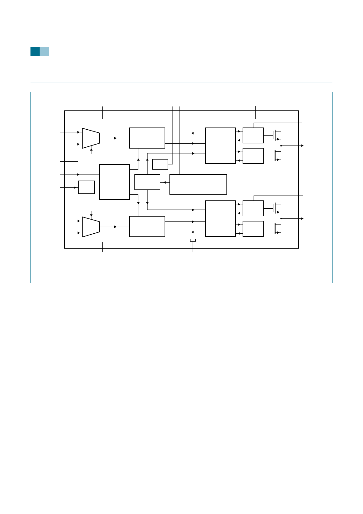
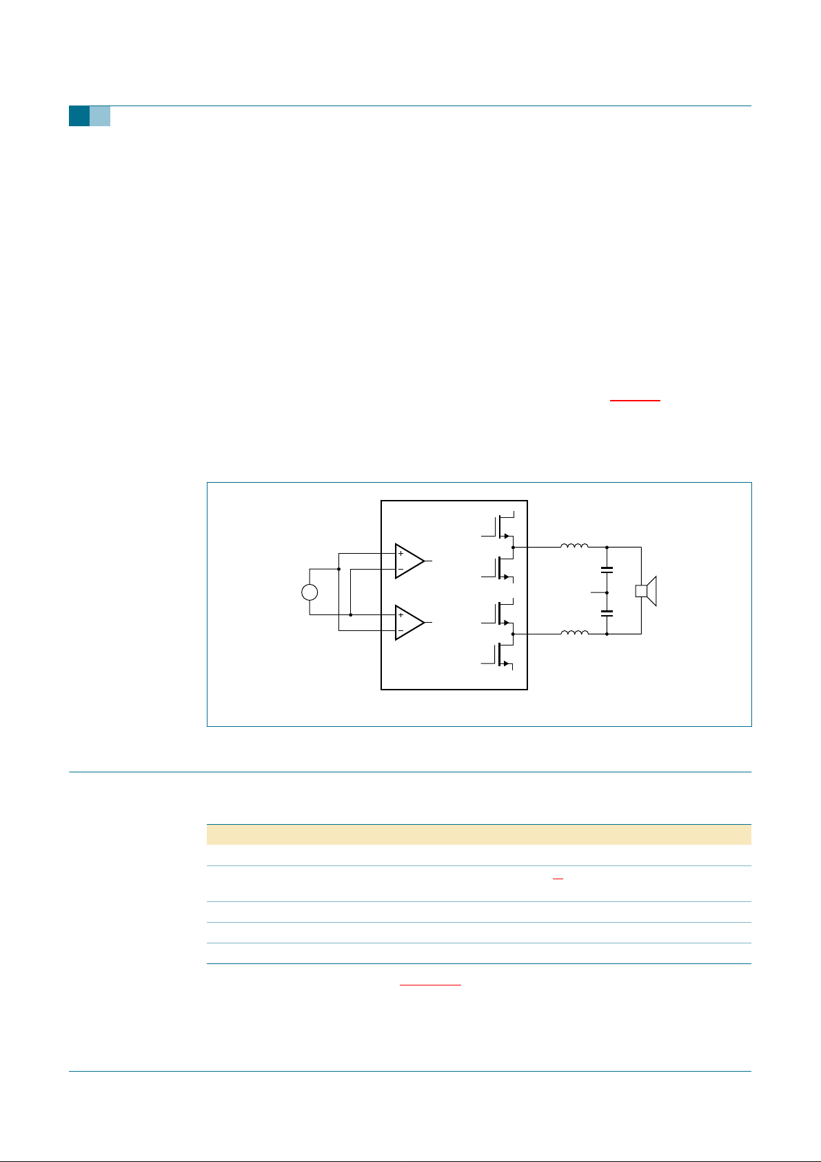
6. Block diagram
Pin numbers in parenthesis refer to the TDA8920BJ.
Fig 1. Block diagram.
coa023
OUT1
V
SSP1
V
DDP2
DRIVER
HIGH
OUT2
BOOT2
TDA8920BTH
(TDA8920BJ)
BOOT1
DRIVER
LOW
RELEASE1
SWITCH1
ENABLE1
CONTROL
AND
HANDSHAKE
PWM
MODULATOR
MANAGER
OSCILLATOR
TEMPERATURE SENSOR
CURRENT PROTECTION
VOLTAGE PROTECTION
STABI
MODE
INPUT
STAGE
mute
9 (3)
8 (2)
IN1M
IN1P
22 (15)
21 (14)
20 (13)
17 (11)
16 (10)
15 (9)
V
SSP2
V
SSP1
DRIVER
HIGH
DRIVER
LOW
RELEASE2
SWITCH2
ENABLE2
CONTROL
AND
HANDSHAKE
PWM
MODULATOR
11 (5)
SGND1
7 (1)
OSC
2 (19)
SGND2
6 (23)
MODE
INPUT
STAGE
mute
5 (22)
4 (21)
IN2M
IN2P
19 (-)24 (17)
V
SSD
n.c.
1 (18)
V
SSA2
12 (6)
V
SSA1
3 (20)
V
DDA2
10 (4)
V
DDA1
23 (16)13 (7)18 (12) 14 (8)
V
DDP2
PROTSTABI
V
DDP1
9397 750 13356 © Koninklijke Philips Electronics N.V. 2004. All rights reserved.
Preliminary data sheet Rev. 01 — 1 October 2004 4 of 34
Philips Semiconductors
TDA8920B
2 × 100 W class-D power amplifier
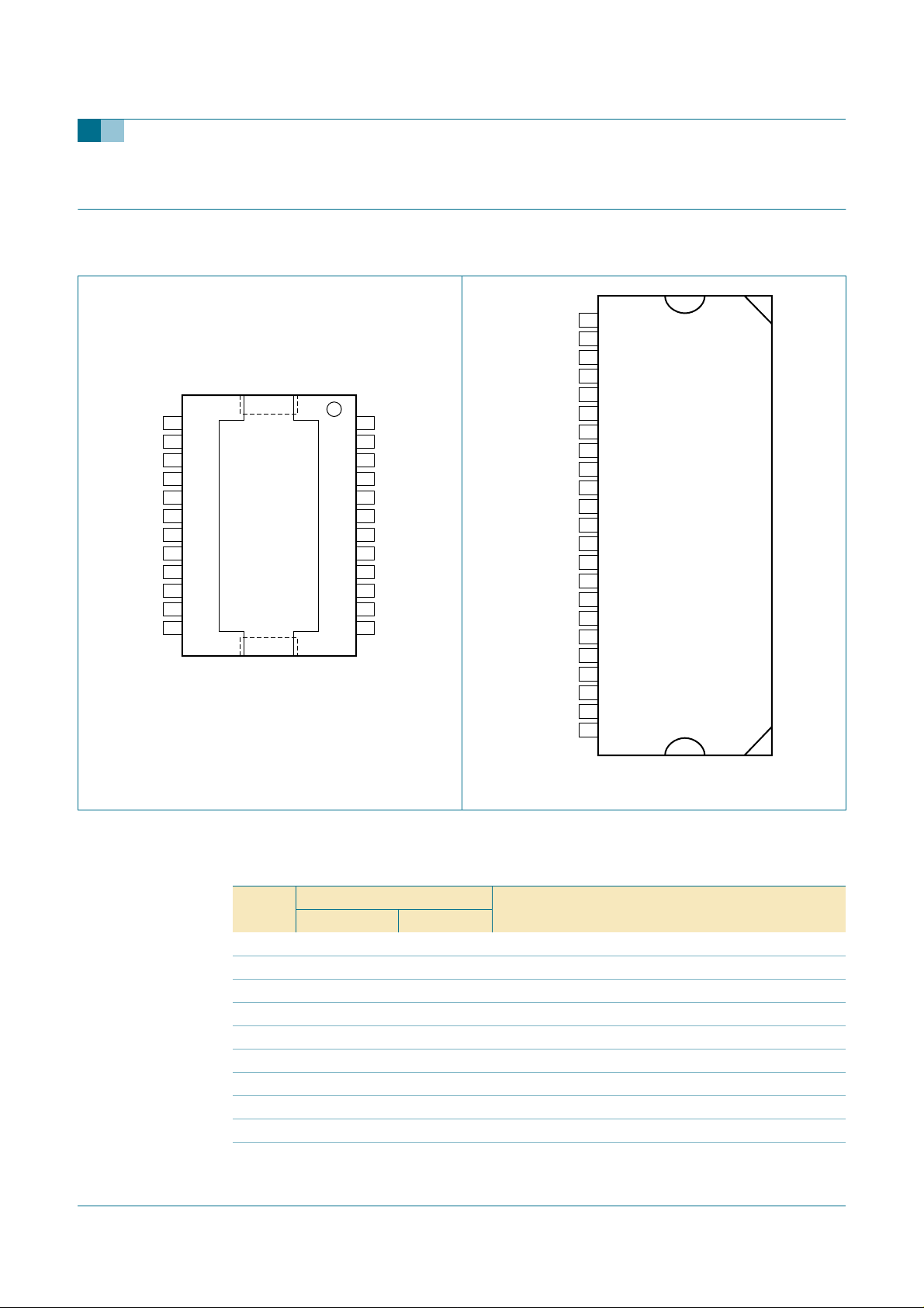
7. Pinning information
7.1 Pinning
7.2 Pin description
Fig 2. Pin configuration TDA8920BTH. Fig 3. Pin configuration TDA8920BJ.
TDA8920BTH
V
SSD
V
SSA2
V
DDP2
SGND2
BOOT2 V
DDA2
OUT2 IN2M
V
SSP2
IN2P
n.c. MODE
STABI OSC
V
SSP1
IN1P
OUT1 IN1M
BOOT1 V
DDA1
V
DDP1
SGND1
PROT V
SSA1
001aab217
24
23
22
21
20
19
18
17
16
15
14
13
11
12
9
10
7
8
5
6
3
4
1
2
TDA8920BJ
OSC
IN1P
IN1M
V
DDA1
SGND1
V
SSA1
PROT
V
DDP1
BOOT1
OUT1
V
SSP1
STABI
V
SSP2
OUT2
BOOT2
V
DDP2
V
SSD
V
SSA2
SGND2
V
DDA2
IN2M
IN2P
MODE
001aab218
1
2
3
4
5
6
7
8
9
10
11
12
13
14
15
16
17
18
19
20
21
22
23
Table 3: Pin description
Symbol Pin Description
TDA8920BTH TDA8920BJ
V
SSA2
1 18 negative analog supply voltage for channel 2
SGND2 2 19 signal ground for channel 2
V
DDA2
3 20 positive analog supply voltage for channel 2
IN2M 4 21 negative audio input for channel 2
IN2P 5 22 positive audio input for channel 2
MODE 6 23 mode selection input: Standby, Mute or Operating mode
OSC 7 1 oscillator frequency adjustment or tracking input
IN1P 8 2 positive audio input for channel 1
IN1M 9 3 negative audio input for channel 1
V
DDA1
10 4 positive analog supply voltage for channel 1

9397 750 13356 © Koninklijke Philips Electronics N.V. 2004. All rights reserved.
Preliminary data sheet Rev. 01 — 1 October 2004 5 of 34
Philips Semiconductors
TDA8920B
2 × 100 W class-D power amplifier
8. Functional description
8.1 General
The TDA8920B is a two channel audio power amplifier using class-D technology.
The audio input signal is converted into a digital Pulse Width Modulated (PWM) signal via
an analog input stage and PWM modulator. To enable the output power transistors to be
driven, this digital PWM signal is applied to a control and handshake block and driver
circuits for both the high side and low side. In this way a level shift is performed from the
low power digital PWM signal (at logic levels) to a high power PWM signal which switches
between the main supply lines.
A 2nd-order low-pass filter converts the PWM signal to an analog audio signal across the
loudspeakers.
The TDA8920B one-chip class-D amplifier contains high power D-MOS switches, drivers,
timing and handshaking between the power switches and some control logic. For
protection a temperature sensor and a maximum current detector are built-in.
The two audio channels of the TDA8920B contain two PWMs, two analog feedback loops
and two differential input stages. It also contains circuits common to both channels such
as the oscillator, all reference sources, the mode functionality and a digital timing
manager.
The TDA8920B contains two independent amplifier channels with high output power,high
efficiency, low distortion and a low quiescent current. The amplifier channels can be
connected in the following configurations:
• Mono Bridge-Tied Load (BTL) amplifier
• Stereo Single-Ended (SE) amplifiers.
SGND1 11 5 signal ground for channel 1
V
SSA1
12 6 negative analog supply voltage for channel 1
PROT 13 7 decoupling capacitor for protection (OCP)
V
DDP1
14 8 positive power supply voltage for channel1
BOOT1 15 9 bootstrap capacitor for channel 1
OUT1 16 10 PWM output from channel 1
V
SSP1
17 11 negative power supply voltage for channel 1
STABI 18 12 decoupling of internal stabilizer for logic supply
n.c. 19 - not connected
V
SSP2
20 13 negative power supply voltage for channel 2
OUT2 21 14 PWM output from channel 2
BOOT2 22 15 bootstrap capacitor for channel 2
V
DDP2
23 16 positive power supply voltage for channel 2
V
SSD
24 17 negative digital supply voltage
Table 3: Pin description
…continued
Symbol Pin Description
TDA8920BTH TDA8920BJ
9397 750 13356 © Koninklijke Philips Electronics N.V. 2004. All rights reserved.
Preliminary data sheet Rev. 01 — 1 October 2004 6 of 34
Philips Semiconductors
TDA8920B
2 × 100 W class-D power amplifier
The amplifier system can be switched in three operating modes with pin MODE:
• Standby mode; with a very low supply current
• Mute mode; the amplifiers are operational; but the audio signal at the output is
suppressed by disabling the VI-converter input stages
• Operating mode; the amplifiers are fully operational with output signal.
To ensure pop-noise free start-up the DC output offset voltage is applied gradually to the
output between Mute mode and Operating mode. The bias current setting of the VI
converters is related to the voltage on the MODE pin; in Mute mode the bias current
setting of the VI converters is zero (VI converters disabled) and in Operating mode the
bias current is at maximum. The time constant required to apply the DC output offset
voltage gradually between mute and operating can be generated via an RC-network on
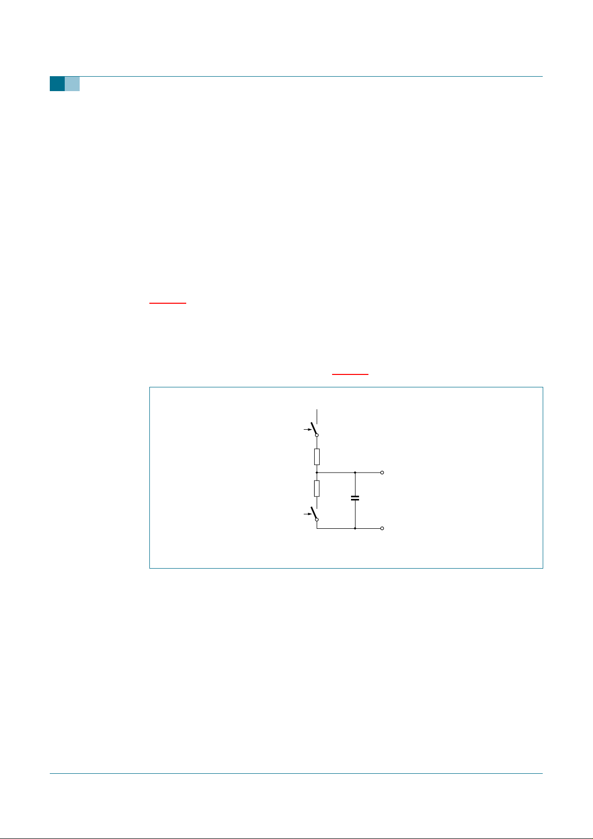
the MODE pin. An example of a switching circuit for driving pin MODE is illustrated in
Figure 4. If the capacitor C is left out of the application the voltage on the MODE pin will
be applied with a much smaller time-constant, which might result in audible pop-noises
during start-up (depending on DC output offset voltage and used loudspeaker).
In order to fully charge the coupling capacitors at the inputs, the amplifier will remain
automatically in the Mute mode before switching to the Operating mode. A complete
overview of the start-up timing is given in Figure 5.
Fig 4. Example of mode selection circuit.
001aab172
SGND
MODE pin
mute/on
R
C
R
+
5 V
standby/
mute
9397 750 13356 © Koninklijke Philips Electronics N.V. 2004. All rights reserved.
Preliminary data sheet Rev. 01 — 1 October 2004 7 of 34
Philips Semiconductors
TDA8920B
2 × 100 W class-D power amplifier
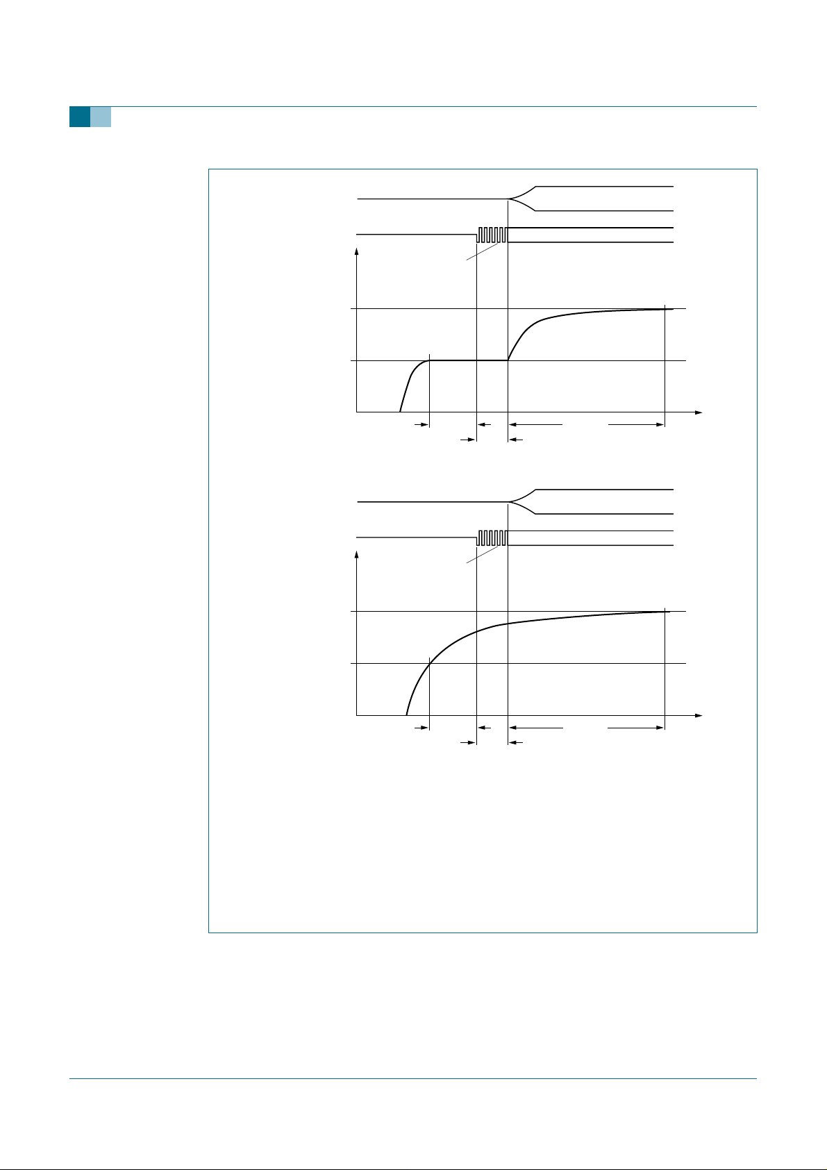
When switching from standby to mute, there is a delay of 100 ms before the output starts
switching. The audio signal is available after V
mode
has been set to operating, but not earlier
than 150 ms after switching to mute. For pop-noise free start-up it is recommended that the
time constant applied to the MODE pin is at least 350 ms for the transition between mute and
operating.
When switching directly from standby to operating, there is a first delay of 100 ms before the
outputs starts switching. The audio signal is available after a second delay of 50 ms. For
pop-noise freestart-up it is recommended that the time constant applied to the MODE pin is at
least 500 ms for the transition between standby and operating.
Fig 5. Timing on mode selection input.
2.2 V < V
mode
< 3 V
audio output
operating
standby
mute
50 %
duty cycle
> 4.2 V
0 V (SGND)
time
coa024
V
mode
100 ms
50 ms
modulated PWM
> 350 ms
2.2 V < V
mode
< 3 V
audio output
operating
standby
mute
50 %
duty cycle
> 4.2 V
0 V (SGND)
time
V
mode
100 ms
50 ms
modulated PWM
> 350 ms

9397 750 13356 © Koninklijke Philips Electronics N.V. 2004. All rights reserved.
Preliminary data sheet Rev. 01 — 1 October 2004 8 of 34
Philips Semiconductors
TDA8920B
2 × 100 W class-D power amplifier
8.2 Pulse width modulation frequency
The output signal of the amplifier is a PWM signal with a carrier frequency of
approximately317 kHz. Using a 2nd-order LC demodulation filter in theapplication results
in an analog audio signal across the loudspeaker. This switching frequency is fixed by an
external resistor R
OSC
connected between pin OSC and V
SSA
. An optimal setting for the
carrier frequency is between 300 kHz and 350 kHz.
Using an external resistor of 30 kΩ on the OSC pin, the carrier frequency is set to
317 kHz.
If two or more class-D amplifiers are used in the same audio application, it is advisable to
have all devices operating at the same switching frequency by using an external clock
circuit.
8.3 Protections
The following protections are included in TDA8920B:
• OverTemperature Protection (OTP)
• OverCurrent Protection (OCP)
• Window Protection (WP)
• Supply voltage protections:
– UnderVoltage Protection (UVP)
– OverVoltage Protection (OVP)
– UnBalance Protection (UBP).
The reaction of the device on the different fault conditions differs per protection:
8.3.1 OverTemperature Protection (OTP)
If the junction temperature T
j
> 150 °C, then the power stage will shut-down immediately.
The power stage will start switching again if the temperature drops to approximately
130 °C, thus there is a hysteresis of approximately 20 °C.
8.3.2 OverCurrent Protection (OCP)
When the loudspeaker terminals are short-circuited or if one of the demodulated outputs
of the amplifier is short-circuited to one of the supply lines, this will be detected by the
OverCurrent Protection (OCP). If the output current exceeds the maximum output current
of 8 A, this current will be limited by the amplifier to 8 A while the amplifier outputs remain
switching (the amplifier is NOT shut-down completely).
The amplifier can distinguish between an impedance drop of the loudspeaker and
low-ohmic short across the load. In the TDA8920B this impedance threshold (Z
th
)
depends on the supply voltage used.
When a short is made across the load causing the impedance to drop below the threshold
level (< Z
th
) then the amplifier is switched off completely and after a time of 100 ms it will
try to restart again. If the short circuit condition is still present after this time this cycle will
be repeated. The average dissipation will be low because of this low duty cycle.

9397 750 13356 © Koninklijke Philips Electronics N.V. 2004. All rights reserved.
Preliminary data sheet Rev. 01 — 1 October 2004 9 of 34
Philips Semiconductors
TDA8920B
2 × 100 W class-D power amplifier
In case of an impedance drop (e.g. due to dynamic behavior of the loudspeaker) the same
protection will be activated; the maximum output current is again limited to 8 A, but the
amplifier will NOT switch-off completely (thus preventing audio holes from occurring).
Result will be a clipping output signal without any artefacts.
See also Section 13.6 for more information on this maximum output current limiting
feature.

9397 750 13356 © Koninklijke Philips Electronics N.V. 2004. All rights reserved.
Preliminary data sheet Rev. 01 — 1 October 2004 10 of 34
Philips Semiconductors
TDA8920B
2 × 100 W class-D power amplifier
8.3.3 Window Protection (WP)
During the start-up sequence, when pin MODE is switched from standby to mute, the
conditions at the output terminals of the power stage are checked. In the event of a
short-circuit at one of the output terminals to V
DD
or V
SS
the start-up procedure is
interrupted and the system waits for open-circuit outputs. Because the test is done before
enabling the power stages, no large currents will flow in the event of a short-circuit. This
system is called Window Protection (WP) and protects for short-circuits at both sides of
the output filter to both supply lines. When there is a short-circuit from the power PWM
output of the power stage to one of the supply lines (before the demodulation filter) it will
also be detected by the start-up safety test. Practical use of this test feature can be found
in detection of short-circuits on the printed-circuit board.
Remark: This test is operational during (every) start-up sequence at a transition between
Standby and Mute mode. However when the amplifier is completely shut-down due to
activation of the OverCurrent Protection (OCP) because a short to one of the supply lines
is made, then during restart (after 100 ms) the window protection will be activated. As a
result the amplifier will not start-up until the short to the supply lines is removed.
8.3.4 Supply voltage protections
If the supply voltage drops below ±12.5 V, the UnderVoltage Protection (UVP) circuit is
activated and the system will shut-down correctly. If the internal clock is used, this
switch-off will be silent and without pop noise. When the supply voltage rises above the
threshold level, the system is restarted again after 100 ms. If the supply voltage exceeds
±33 V the OverVoltage Protection (OVP) circuit is activated and the power stages will
shut-down. It is re-enabled as soon as the supply voltage drops below the threshold level.
So in this case no timer of 100 ms is started.
An additional UnBalance Protection (UBP) circuit compares the positive analog (V
DDA
)
and the negative analog (V
SSA
) supply voltages and is triggered if the voltage difference
between them exceeds a certain level. This level depends on the sum of both supply
voltages. An expression for the unbalanced threshold level is as follows:
V
th(ub)
≈ 0.15 × (V
DDA
+V
SSA
).
When the supply voltage difference drops below the threshold level, the system is
restarted again after 100 ms.
Example: With a symmetrical supply of ±30 V, the protection circuit will be triggered if the
unbalance exceeds approximately 9 V; see also Section 13.7.
In Table 4 an overview is given of all protections and the effect on the output signal.
[1] Hysteresis of 20 degrees will influence restart timing depending on heatsink size.
Table 4: Overview protections TDA8920B
Protection name Complete shut-down Restart directly Restart every 100 ms
OTP Y Y
[1]
N
[1]
OCP N
[2]
Y
[2]
N
[2]
WP Y
[3]
YN
UVP Y N Y
OVPYYN
UBP Y N Y
9397 750 13356 © Koninklijke Philips Electronics N.V. 2004. All rights reserved.
Preliminary data sheet Rev. 01 — 1 October 2004 11 of 34
Philips Semiconductors
TDA8920B
2 × 100 W class-D power amplifier
[2] Only complete shut-down of amplifier if short-circuit impedance is below threshold of 1 Ω. In all other cases
current limiting: resulting in clipping output signal.
[3] Fault condition detected during (every) transition between standby-to-mute and during restart after
activation of OCP (short to one of the supply lines).
8.4 Differential audio inputs
Fora high common mode rejection ratio and a maximum of flexibility in the application, the
audio inputs are fully differential. By connecting the inputs anti-parallel the phase of one of
the channels can be inverted, so that a load can be connected between the two output
filters. In this case the system operates as a mono BTL amplifier and with the same
loudspeaker impedance an approximately four times higher output power can be
obtained.
The input configuration for a mono BTL application is illustrated in Figure 6.
In the stereo single-ended configuration it is also recommended to connect the two
differential inputs in anti-phase. This has advantages for the current handling of the power
supply at low signal frequencies.
9. Limiting values
[1] Current limiting concept. See also Section 13.6.
Fig 6. Input configuration for mono BTL application.
V
in
IN1P
OUT1
power stage
mbl466
OUT2
SGND
IN1M
IN2P
IN2M
Table 5: Limiting values
In accordance with the Absolute Maximum Rating System (IEC 60134).
Symbol Parameter Conditions Min Max Unit
V
P
supply voltage - ±30 V
I
ORM
repetitive peak current in
output pin
maximum output
current limiting
[1]
8- A
T
stg
storage temperature −55 +150 °C
T
amb
ambient temperature −40 +85 °C
T
j
junction temperature - 150 °C
Loading...