


INTEGRATED CIRCUITS
DATA SHEET
TDA1575T
FM front end circuit for CENELEC EN 55020 applications
Preliminary specification |
|
April 1993 |
|||||
Supersedes data of October 1990 |
|
|
|
|
|
|
|
File under Integrated Circuits, IC01 |
|
|
|
|
|
|
|
|
|
|
|
|
|
|
|
|
|
|
|
|
|
|
|
|
|
|
|
|
|
|
|

Philips Semiconductors |
Preliminary specification |
|
|
FM front end circuit for
TDA1575T
CENELEC EN 55020 applications
FEATURES
∙Bipolar integrated FM front end circuit, designed for use in car radios and home receivers
∙Fulfils CENELEC EN 55020 requirements
∙Radio frequency range of 76 to 90 MHz (Japan) or
87.5 to 108 MHz (Europe, USA)
∙Low noise oscillator, buffered oscillator output
∙Double balanced mixer
∙Internal buffered mixer driving
∙Linear IF amplifier, suitable for ceramic IF filters
∙Regulated reference voltage.
QUICK REFERENCE DATA
SYMBOL |
|
|
PARAMETER |
|
|
MIN. |
TYP. |
MAX. |
UNIT |
||
|
|
|
|
|
|
|
|
|
|
|
|
VP |
supply voltage |
|
|
|
|
7 |
8.5 |
|
10 |
V |
|
IP |
supply current, without mixer |
|
|
− |
23 |
|
− |
mA |
|||
VREF |
reference voltage output |
|
|
− |
4.2 |
|
− |
V |
|||
ZI |
mixer input impedance |
|
|
− |
14 |
|
− |
Ω |
|||
NF |
noise figure of mixer |
|
|
− |
9 |
|
− |
dB |
|||
|
|
|
|
|
|
|
|
|
|
|
|
EMF1 |
3rd order intermodulation |
|
|
− |
115 |
|
− |
dBμV |
|||
|
|
|
|
|
|
|
|
|
|
||
VOSC |
oscillator buffer output signal (RMS value) |
75 |
− |
− |
mV |
||||||
THD |
total harmonic distortion |
|
|
− |
−15 |
− |
dBC |
||||
|
|
|
|
|
|
|
|
|
|
|
|
Gv |
IF gain |
|
|
|
|
− |
30 |
|
− |
dB |
|
NF |
IF noise figure |
|
|
|
|
− |
6.5 |
|
− |
dB |
|
|
|
|
|
|
|
|
|
|
|
|
|
ZI |
IF input impedance |
|
|
− |
300 |
|
− |
Ω |
|||
ZO |
IF output impedance |
|
|
− |
300 |
|
− |
Ω |
|||
EMF2 |
AGC wideband threshold (RMS value) |
− |
17 |
|
− |
mV |
|||||
|
|
|
|
|
|
|
|
|
|
|
|
ORDERING INFORMATION |
|
|
|
|
|
|
|
|
|
||
|
|
|
|
|
|
|
|
|
|
|
|
EXTENDED |
|
|
|
PACKAGE |
|
|
|
|
|||
|
|
|
|
|
|
|
|
|
|
||
TYPE NUMBER |
|
PINS |
|
PIN POSITION |
|
MATERIAL |
|
CODE |
|||
|
|
|
|
|
|
||||||
|
|
|
|
|
|
|
|
|
|||
TDA1575T |
|
16 |
|
mini-pack |
|
plastic |
|
SOT109A(1) |
|||
Note
1. SOT109-1; 1996 August 29.
April 1993 |
2 |
 TDA1575T Schematic")
Philips Semiconductors |
Preliminary specification |
|
|
FM front end circuit for
TDA1575T
CENELEC EN 55020 applications
Coils TOKO
L1: MC-108 514 HNE-150023S14; L = 78 nH, N = 4 turns
L2: MC-111 E516 HNS-200057; L = 80 nH
L3: A119 ACS-17114 FTT
Fig.1 Block diagram and test circuit.
April 1993 |
3 |
Philips Semiconductors |
Preliminary specification |
|
|
FM front end circuit for
TDA1575T
CENELEC EN 55020 applications
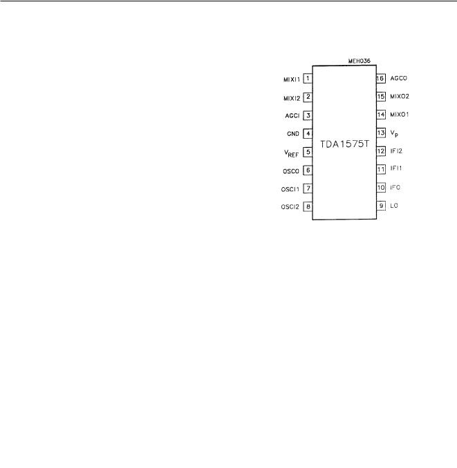
PINNING |
|
|
|
|
|
|
|
|
|
SYMBOL |
PIN |
DESCRIPTION |
|
|
|
|
|
|
|
MIXI1 |
1 |
RF input 1 to mixer |
|
|
|
|
|
|
|
MIXI2 |
2 |
RF input 2 to mixer |
|
|
|
|
|
|
|
AGCI |
3 |
HF input to automatic gain control |
|
|
|
|
|
|
|
GND |
4 |
ground (0 V) |
|
|
|
|
|
|
|
VREF |
5 |
reference voltage output |
|
|
OSCO |
6 |
oscillator output |
|
|
|
|
|
|
|
OSCI1 |
7 |
oscillator input 1 |
|
|
|
|
|
|
|
OSCI2 |
8 |
oscillator input 2 |
|
|
|
|
|
|
|
LO |
9 |
buffered oscillator output |
|
|
|
|
|
|
|
IFO |
10 |
linear FM IF output |
|
|
|
|
|
|
|
IFI1 |
11 |
FM IF input 1 |
|
|
|
|
|
|
|
IFI2 |
12 |
FM IF input 2 |
|
|
|
|
|
|
|
VP |
13 |
supply voltage (+8.5 V) |
|
|
MIXO1 |
14 |
mixer output 1 |
|
|
|
|
|
|
|
MIXO2 |
15 |
mixer output 2 |
|
Fig.2 Pin configuration. |
|
|
|
|
|
AGCO |
16 |
automatic gain control output |
|
|
|
|
|
|
|
LIMITING VALUES
Limiting values in accordance with the Absolute Maximum System (IEC 134).
SYMBOL |
PARAMETER |
MIN. |
MAX. |
UNIT |
|
|
|
|
|
VP |
supply voltage (pin 13) |
0 |
12 |
V |
V14, 15 |
voltage at mixer output |
0 |
VP |
V |
Ptot |
total power dissipation |
0 |
380 |
mW |
Tstg |
storage temperature range |
−55 |
+150 |
°C |
Tamb |
operating ambient temperature range |
−40 |
+85 |
°C |
VESD |
electrostatic handling (see note 1) |
|
|
|
|
all pins except 3 and 10 |
− |
±2000 |
V |
|
pin 3 |
− |
+2000 |
V |
|
|
− |
−1000 |
V |
|
pin 10 |
− |
+1500 |
V |
|
|
− |
−2000 |
V |
|
|
|
|
|
Note to the limiting values
1. Equivalent to discharging a 100 pF capacitor through a 1.5 kΩ series resistor.
April 1993 |
4 |

Philips Semiconductors |
Preliminary specification |
|
|
FM front end circuit for
TDA1575T
CENELEC EN 55020 applications
CHARACTERISTICS
VP = 8.5 V and Tamb = +25°C, measurements taken in Fig.1 with f0 = 98 MHz (EMF1) unless otherwise specified.
SYMBOL |
PARAMETER |
CONDITIONS |
MIN. |
TYP. |
MAX. |
UNIT |
|
|
|
|
|
|
|
VP |
supply voltage (pin 13) |
|
7 |
8.5 |
10 |
V |
IP |
supply current |
without mixer |
16 |
23 |
30 |
mA |
VREF |
reference voltage (pin 5) |
I5 £ 3 mA |
3.9 |
4.2 |
4.4 |
V |
Mixer |
|
|
|
|
|
|
|
|
|
|
|
|
|
I14+15 |
mixer supply current (pins 14 and 15) |
|
- |
4 |
- |
mA |
V1,2 |
DC voltage input (pins 1 and 2) |
|
- |
1 |
- |
V |
Z1,2 |
input impedance |
|
- |
14 |
- |
W |
V14,15 |
DC output voltage (pins 14 and 15) |
|
4 |
- |
10 |
V |
C14,15 |
output capacitance |
|
- |
13 |
- |
pF |
GP |
conversion power gain |
note 1 |
- |
14 |
- |
dB |
EMF1IP3 |
3rd order intercept point |
|
- |
115 |
- |
dBmV |
NF |
noise figure |
|
- |
9 |
- |
dB |
|
total noise figure |
including |
- |
11 |
- |
dB |
|
|
transforming network |
|
|
|
|
|
|
|
|
|
|
|
Oscillator |
|
|
|
|
|
|
|
|
|
|
|
|
|
V7,8 |
DC input voltage (pins 7 and 8) |
|
- |
1.3 |
- |
V |
V6 |
DC output voltage (pin 6) |
|
- |
2.0 |
- |
V |
Df |
residual FM at pin 6 |
f = 300 to 15000 Hz; |
- |
2.2 |
- |
Hz |
|
|
de-emphasis 50 ms |
|
|
|
|
Oscillator buffered output (pin 9) |
|
|
|
|
|
|
|
|
|
|
|
|
|
VO |
output signal (RMS value) |
RL= 500 W; CL= 2 pF |
75 |
- |
- |
mV |
V9 |
DC output voltage |
|
- |
6 |
- |
V |
R9 |
DC output resistor |
|
- |
950 |
- |
W |
THD |
total harmonic distortion |
|
- |
-15 |
- |
dBC |
fS |
spurious frequencies |
EMF1 = 2 V; |
- |
-37 |
- |
dBC |
|
|
RS = 50 W; |
|
|
|
|
|
|
fOSC = 108.7 MHz |
|
|
|
|
Automatic gain control (AGC) |
|
|
|
|
|
|
|
|
|
|
|
|
|
R3 |
input resistance (pin 3) |
|
- |
4 |
- |
kW |
C3 |
input capacitance |
|
- |
3 |
- |
pF |
V16 |
AGC output swing (DC) |
Figs 3 and 4 |
0.5 |
- |
VP - 0.3 |
V |
I16 |
output current at I3 = 0 |
V16 = 1¤2VP |
-25 |
-50 |
-150 |
mA |
|
output current at U3 = 2 V |
V16 = 7 to 10 V |
2 |
- |
5 |
mA |
EMF2 |
threshold (RMS value) |
I16 = 0; V16 = 1¤2VP; |
- |
17 |
- |
mV |
|
|
Figs 4 and 5 |
|
|
|
|
|
|
|
|
|
|
|
April 1993 |
5 |
Philips Semiconductors |
Preliminary specification |
|
|
FM front end circuit for
TDA1575T
CENELEC EN 55020 applications
SYMBOL |
PARAMETER |
CONDITIONS |
MIN. |
TYP. |
MAX. |
UNIT |
|
|
|
|
|
|
|
Linear IF amplifier |
IF = 10.7 MHz |
|
|
|
|
|
|
|
|
|
|
|
|
V11,12 |
DC input voltage (pins 11 and 12) |
|
− |
1.25 |
− |
V |
Z12-11 |
input impedance |
|
240 |
300 |
360 |
Ω |
C12-11 |
input capacitance |
|
− |
13 |
− |
pF |
V10 |
DC output voltage (pin 10) |
|
− |
4.4 |
− |
V |
Z10 |
output impedance |
|
240 |
300 |
360 |
Ω |
C10 |
output capacitance |
|
− |
3 |
− |
pF |
VO |
output signal (RMS value) |
−1 dB compression |
− |
− |
650 |
mV |
Gv |
IF voltage gain (20 log (V10−4 / V12−11)) |
|
27 |
30 |
− |
dB |
Gv |
IF voltage gain deviation |
Tamb= −40 to +85 °C |
− |
0 |
− |
dB |
NF |
noise figure |
RS = 300 Ω |
− |
6.5 |
− |
dB |
Note
1. GP = 10 log (4Vo mix ×10.7 MHz) / (EMF2 × 98 MHz)2 × (RS1 / RML).
Fig.3 AGC output voltage V16 as a function of |
|
Fig.4 AGC output current I16 as a function of |
Vi3 RMS at I16 = 0, measured in test circuit |
|
Vi3 RMS at V16 = 8.5 V, measured in test |
Fig.1. |
|
circuit Fig.1. |
|
|
|
April 1993 |
6 |
 Loading...