


 Loading...
INTEGRATED CIRCUITS
DATA SHEET
TDA8588J; TDA8588xJ
I2C-bus controlled 4 × 50 Watt power amplifier and multiple voltage regulator
Product specification |
|
2004 Feb 24 |
|||||
|
|
|
|
|
|
|
|
|
|
|
|
|
|
|
|
|
|
|
|
|
|
|
|

Philips Semiconductors |
Product specification |
|
|
I2C-bus controlled 4 × 50 Watt power
TDA8588J; TDA8588xJ
amplifier and multiple voltage regulator
FEATURES
Amplifiers
•I2C-bus control
•Can drive a 2 Ω load with a battery voltage of up to 16 V and a 4 Ω load with a battery voltage of up to 18 V
•DC load detection, open, short and present
•AC load (tweeter) detection
•Programmable clip detect; 1 % or 4 %
•Programmable thermal protection pre-warning
•Independent short-circuit protection per channel
•Low gain line driver mode (20 dB)
•Loss-of-ground and open VP safe
•All outputs protected from short-circuit to ground, to VP or across the load
•All pins protected from short-circuit to ground
•Soft thermal-clipping to prevent audio holes
•Low battery detection.
Voltage regulators
GENERAL
•I2C-bus control
•Good stability for any regulator with almost any output capacitor value
•Five voltage regulators (microcontroller, display, mechanical digital, mechanical drive and audio)
•Choice of non-adjustable 3.3 or 5 V microcontroller supply (REG2) versions reducing risk of overvoltage damage
•Choice of non-adjustable 3.3 or 5 V digital signal processor supply (REG3) versions reducing risk of overvoltage damage
•Selectable output voltages for regulators 1, 4 and 5
•Low dropout voltage PNP output stages
•High supply voltage ripple rejection
•Low noise for all regulators
•Two power switches (antenna switch and amplifier switch)
•Regulator 2 (microcontroller supply) operational during load-dump and thermal shut-down
•Low quiescent current (only regulator 2 is operational)
•Reset output (push-pull output stage)
•Adjustable reset delay time
•Backup functionality.
PROTECTION
•If connection to the battery voltage is reversed, all regulator voltages will be zero
•Able to withstand voltages at the output of up to 18 V (supply line may be short-circuited)
•Thermal protection to avoid thermal breakdown
•Load-dump protection
•Regulator outputs protected from DC short-circuit to ground or to supply voltage
•All regulators protected by foldback current limiting
•Power switches protected from loss-of-ground.
APPLICATIONS
•Boost amplifier and voltage regulator for car radios and CD/MD players.
GENERAL DESCRIPTION
Amplifiers
The TDA8588 has a complementary quad audio power amplifier that uses BCDMOS technology. It contains four amplifiers configured in Bridge Tied Load (BTL) to drive speakers for front and rear left and right channels. The I2C-bus allows diagnostic information of each amplifier and its speaker to be read separately. Both front and both rear channel amplifiers can be configured independently in line driver mode with a gain of 20 dB (differential output).
Voltage regulators
The TDA8588 has a multiple output voltage regulator with two power switches.
The voltage regulator contains the following:
•Four switchable regulators and one permanently active regulator (microcontroller supply)
•Two power switches with loss-of-ground protection
•A reset output that can be used to communicate with a microcontroller.
The quiescent current has a very low level of 150 µA with only regulator 2 active.
2004 Feb 24 |
2 |

Philips Semiconductors |
Product specification |
|
|
I2C-bus controlled 4 × 50 Watt power
TDA8588J; TDA8588xJ
amplifier and multiple voltage regulator
QUICK REFERENCE DATA
SYMBOL |
PARAMETER |
CONDITIONS |
MIN. |
TYP. |
MAX. |
UNIT |
|
|
|
|
|
|
|
Amplifiers |
|
|
|
|
|
|
|
|
|
|
|
|
|
VP1, VP2 |
operating supply voltage |
|
8 |
14.4 |
18 |
V |
Iq(tot) |
total quiescent current |
|
− |
270 |
400 |
mA |
Po(max) |
maximum output power |
RL = 4 Ω; VP = 14.4 V; VIN = 2 V |
44 |
46 |
− |
W |
|
|
RMS square wave |
|
|
|
|
|
|
|
|
|
|
|
|
|
RL = 4 Ω; VP = 15.2 V; VIN = 2 V |
49 |
52 |
− |
W |
|
|
RMS square wave |
|
|
|
|
|
|
|
|
|
|
|
|
|
RL = 2 Ω; VP = 14.4 V; VIN = 2 V |
83 |
87 |
− |
W |
|
|
RMS square wave |
|
|
|
|
|
|
|
|
|
|
|
THD |
total harmonic distortion |
|
− |
0.01 |
0.1 |
% |
|
|
|
|
|
|
|
Vn(o)(amp) |
noise output voltage in amplifier mode |
|
− |
50 |
70 |
µV |
Vn(o)(LN) |
noise output voltage in line driver mode |
|
− |
25 |
35 |
µV |
Voltage regulators |
|
|
|
|
|
|
|
|
|
|
|
|
|
SUPPLY |
|
|
|
|
|
|
|
|
|
|
|
|
|
VP |
supply voltage |
regulator 1, 3, 4 and 5 on |
10 |
14.4 |
18 |
V |
|
|
regulator 2 on |
4 |
− |
− |
V |
|
|
|
|
|
|
|
|
|
jump starts for t ≤ 10 minutes |
− |
− |
30 |
V |
|
|
|
|
|
|
|
|
|
load dump protection for |
− |
− |
50 |
V |
|
|
t ≤ 50 ms and tr ≤ 2.5 ms |
|
|
|
|
|
|
overvoltage for shut-down |
20 |
− |
− |
V |
|
|
|
|
|
|
|
Iq(tot) |
total quiescent supply current |
standby mode; VP = 14.4 V |
− |
150 |
190 |
µA |
VOLTAGE REGULATORS |
|
|
|
|
|
|
|
|
|
|
|
|
|
VO(REG1) |
output voltage of regulator 1 |
0.5 mA ≤ IO ≤ 400 mA; |
|
|
|
|
|
|
selectable via I2C-bus |
|
|
|
|
|
|
IB2[D3:D2] = 01 |
− |
8.3 |
− |
V |
|
|
IB2[D3:D2] = 10 |
− |
8.5 |
− |
V |
|
|
IB2[D3:D2] = 11 |
− |
8.7 |
− |
V |
|
|
|
|
|
|
|
VO(REG2) |
output voltage of regulator 2 |
0.5 mA ≤ IO ≤ 350 mA |
|
|
|
|
|
|
TDA8588J; TDA8588AJ |
− |
5.0 |
− |
V |
|
|
TDA8588BJ |
− |
3.3 |
− |
V |
|
|
|
|
|
|
|
VO(REG3) |
output voltage of regulator 3 |
0.5 mA ≤ IO ≤ 300 mA |
|
|
|
|
|
|
TDA8588J |
− |
5.0 |
− |
V |
|
|
TDA8588AJ; TDA8588BJ |
− |
3.3 |
− |
V |
|
|
|
|
|
|
|
VO(REG4) |
output voltage of regulator 4 |
maximum current ≥ 1.6 A; |
|
|
|
|
|
|
0.5 mA ≤ IO ≤ 800 mA; |
|
|
|
|
|
|
selectable via I2C-bus |
|
|
|
|
|
|
IB2[D7:D5] = 001 |
− |
5.0 |
− |
V |
|
|
IB2[D7:D5] = 010 |
− |
6.0 |
− |
V |
|
|
IB2[D7:D5] = 011 |
− |
7.0 |
− |
V |
|
|
IB2[D7:D5] = 100 |
− |
8.6 |
− |
V |
|
|
|
|
|
|
|
2004 Feb 24 |
3 |

Philips Semiconductors |
Product specification |
|
|
I2C-bus controlled 4 × 50 Watt power
TDA8588J; TDA8588xJ
amplifier and multiple voltage regulator
SYMBOL |
|
PARAMETER |
|
CONDITIONS |
|
MIN. |
TYP. |
MAX. |
UNIT |
||||
|
|
|
|
|
|
|
|
|
|
|
|
|
|
VO(REG5) |
output voltage of regulator 5 |
|
0.5 mA ≤ IO ≤ 400 mA; |
|
|
|
|
|
|
|
|||
|
|
|
|
|
selectable via I2C-bus |
|
|
|
|
|
|
|
|
|
|
|
|
|
IB1[D7:D4] = 0001 |
|
− |
6.0 |
|
− |
|
V |
|
|
|
|
|
|
IB1[D7:D4] = 0010 |
|
− |
7.0 |
|
− |
|
V |
|
|
|
|
|
|
IB1[D7:D4] = 0011 |
|
− |
8.2 |
|
− |
|
V |
|
|
|
|
|
|
IB1[D7:D4] = 0100 |
|
− |
9.0 |
|
− |
|
V |
|
|
|
|
|
|
IB1[D7:D4] = 0101 |
|
− |
9.5 |
|
− |
|
V |
|
|
|
|
|
|
IB1[D7:D4] = 0110 |
|
− |
10.0 |
− |
|
V |
||
|
|
|
|
|
IB1[D7:D4] = 0111 |
|
− |
10.4 |
− |
|
V |
||
|
|
|
|
|
IB1[D7:D4] = 1000 |
|
− |
12.5 |
− |
|
V |
||
|
|
|
|
|
IB1[D7:D4] = 1001 |
|
− |
VP − |
− |
|
V |
||
|
|
|
|
|
|
|
|
|
1 |
|
|
|
|
|
|
|
|
|
|
|
|
|
|
|
|
|
|
POWER SWITCHES |
|
|
|
|
|
|
|
|
|
|
|||
|
|
|
|
|
|
|
|
|
|
|
|
|
|
Vdrop(SW1) |
dropout voltage of switch 1 |
|
IO = 400 mA |
|
|
− |
0.6 |
|
1.1 |
|
V |
||
Vdrop(SW2) |
dropout voltage of switch 2 |
|
IO = 400 mA |
|
|
− |
0.6 |
|
1.1 |
|
V |
||
ORDERING INFORMATION |
|
|
|
|
|
|
|
|
|
|
|||
|
|
|
|
|
|
|
|
|
|
||||
TYPE NUMBER |
|
|
PACKAGE |
|
|
OUTPUT VOLTAGE(1) |
|
||||||
NAME |
|
DESCRIPTION |
VERSION |
REGULATOR 2 |
REGULATOR 3 |
||||||||
|
|
|
|||||||||||
|
|
|
|
|
|
|
|
|
|
|
|||
TDA8588J |
|
DBS37P |
plastic DIL-bent-SIL power package; |
SOT725-1 |
|
5 V |
|
|
5 V |
|
|||
|
|
|
37 leads (lead length 6.8 mm) |
|
|
|
|
|
|
|
|
||
TDA8588AJ |
|
|
|
|
5 V |
|
|
3.3 V |
|
||||
|
|
|
|
|
|
|
|
|
|
||||
|
|
|
|
|
|
|
|
|
|
|
|
|
|
TDA8588BJ |
|
|
|
|
|
|
|
3.3 V |
|
|
3.3 V |
|
|
|
|
|
|
|
|
|
|
|
|
|
|
|
|
Note
1. Permanent output voltage of regulator 2 and output voltage of regulator 3, respectively.
2004 Feb 24 |
4 |
 TDA8588AJ, TDA8588BJ, TDA8588J Schematic")
Philips Semiconductors |
Product specification |
|
|
I2C-bus controlled 4 × 50 Watt power
TDA8588J; TDA8588xJ
amplifier and multiple voltage regulator
BLOCK DIAGRAM
BUCAP |
36 |
|
|
|
REGULATOR 2 |
|
37 |
REG2 |
|
|
|
|
|
|
|
||||
|
|
|
REFERENCE |
|
TEMPERATURE & |
|
|||
|
BACKUP |
|
|
LOAD DUMP |
|
||||
|
SWITCH |
|
VOLTAGE |
|
PROTECTION VOLTAGE |
|
|||
|
|
|
|
|
|
REGULATOR |
|
||
VP |
35 |
|
|
|
REGULATOR 1 |
|
30 |
|
|
|
|
|
|
|
REG1 |
||||
|
|
|
|
|
|
|
|
|
|
|
|
TDA8588 |
|
|
REGULATOR 3 |
|
31 |
REG3 |
|
|
|
ENABLE |
|
|
REGULATOR 4 |
|
33 |
REG4 |
|
|
|
|
|
|
|
|
|
||
|
|
|
|
|
|
|
|
|
|
|
|
LOGIC |
|
|
|
|
|
|
|
|
|
|
|
|
REGULATOR 5 |
|
34 |
REG5 |
|
|
|
|
Vreg2 |
|
|
|
|
||
|
|
|
|
|
|
|
|
||
|
|
|
|
|
|
SWITCH 1 |
|
29 |
|
|
|
|
|
|
|
|
|
SW1 |
|
|
|
|
|
|
|
|
|
|
|
|
|
|
|
|
|
SWITCH 2 |
|
27 |
|
|
|
40 µs |
|
|
|
|
|
SW2 |
|
|
|
|
|
|
|
|
|
||
RESCAP |
28 |
|
|
|
|
|
|
|
|
|
|
|
|
|
|
|
26 |
|
|
|
|
|
|
|
|
|
|
RST |
|
|
|
|
|
|
|
|
|
|
|
|
|
|
|
|
|
|
|
32 |
GND |
|
|
|
|
|
|
|
|
|
|
|
2 |
|
|
|
|
|
|
20 |
VP1 |
SDA |
|
|
|
|
|
|
6 |
||
|
4 |
|
|
|
|
|
|
VP2 |
|
SCL |
|
|
|
|
|
|
|
||
|
|
|
|
|
|
|
25 |
DIAG |
|
|
|
|
|
|
|
|
|
||
|
22 |
|
I2C-BUS |
|
|
|
|
||
STB |
|
CLIP DETECT/ DIAGNOSTIC |
|
||||||
STANDBY/ MUTE |
INTERFACE |
|
|||||||
|
|
|
|
|
|
|
|
||
IN1 |
11 |
|
MUTE |
26 dB/ |
|
|
|
9 |
OUT1+ |
|
|
|
|
|
|
7 |
|||
|
|
|
|
20 dB |
|
|
|
OUT1− |
|
|
|
|
|
|
|
|
|
|
|
|
|
|
|
|
|
PROTECTION/ |
|
|
|
|
|
|
|
|
|
DIAGNOSTIC |
17 |
|
|
IN2 |
15 |
|
MUTE |
26 dB/ |
|
|
|
OUT2+ |
|
|
|
|
|
|
|
19 |
|||
|
|
|
|
20 dB |
|
|
|
OUT2− |
|
|
|
|
|
|
|
|
|
|
|
|
|
|
|
|
|
PROTECTION/ |
|
|
|
|
|
|
|
|
|
DIAGNOSTIC |
5 |
|
|
IN3 |
12 |
|
MUTE |
26 dB/ |
|
|
|
OUT3+ |
|
|
|
|
|
|
|
3 |
|||
|
|
|
|
20 dB |
|
|
|
OUT3− |
|
|
|
|
|
|
|
|
|
|
|
|
|
|
|
|
|
PROTECTION/ |
|
|
|
|
|
|
|
|
|
DIAGNOSTIC |
21 |
|
|
IN4 |
14 |
|
MUTE |
26 dB/ |
|
|
|
OUT4+ |
|
|
|
|
|
|
|
23 |
|||
|
VP |
|
|
20 dB |
|
|
|
OUT4− |
|
|
|
|
|
|
|
|
|
||
|
|
|
|
|
|
PROTECTION/ |
|
|
|
|
|
|
|
|
|
DIAGNOSTIC |
|
|
|
|
|
|
|
TEMPERATURE & LOAD |
|
||||
|
|
|
|
|
DUMP PROTECTION |
|
|
||
|
|
|
|
|
|
AMPLIFIER |
|
|
|
|
10 |
|
13 |
16 |
8 |
1 |
18 |
24 |
mdb586 |
|
SVR |
SGND |
PGND1 |
PGND3 |
|
|
|||
|
|
|
|
ACGND |
PGND2/TAB |
|
PGND4 |
|
|
Fig.1 Block diagram.
2004 Feb 24 |
5 |

Philips Semiconductors |
Product specification |
|
|
I2C-bus controlled 4 × 50 Watt power
TDA8588J; TDA8588xJ
amplifier and multiple voltage regulator
PINNING
|
SYMBOL |
PIN |
DESCRIPTION |
|
|
|
|
|
|
|
PGND2/TAB |
1 |
power ground 2 and connection for heatsink |
|
|
|
|
|
|
|
SDA |
2 |
I2C-bus data input and output |
|
|
OUT3− |
3 |
channel 3 negative output |
|
|
|
|
|
|
|
SCL |
4 |
I2C-bus clock input |
|
|
OUT3+ |
5 |
channel 3 positive output |
|
|
|
|
|
|
|
VP2 |
6 |
power supply voltage 2 to amplifier |
|
|
OUT1− |
7 |
channel 1 negative output |
|
|
|
|
|
|
|
PGND1 |
8 |
power ground 1 |
|
|
|
|
|
|
|
OUT1+ |
9 |
channel 1 positive output |
|
|
|
|
|
|
|
SVR |
10 |
half supply voltage filter capacitor |
|
|
|
|
|
|
|
IN1 |
11 |
channel 1 input |
|
|
|
|
|
|
|
IN3 |
12 |
channel 3 input |
|
|
|
|
|
|
|
SGND |
13 |
signal ground |
|
|
|
|
|
|
|
IN4 |
14 |
channel 4 input |
|
|
|
|
|
|
|
IN2 |
15 |
channel 2 input |
|
|
|
|
|
|
|
ACGND |
16 |
AC ground |
|
|
|
|
|
|
|
OUT2+ |
17 |
channel 2 positive output |
|
|
|
|
|
|
|
PGND3 |
18 |
power ground 3 |
|
|
|
|
|
|
|
OUT2− |
19 |
channel 2 negative output |
|
|
|
|
|
|
|
VP1 |
20 |
power supply voltage 1 to amplifier |
|
|
OUT4+ |
21 |
channel 4 positive output |
|
|
|
|
|
|
|
STB |
22 |
standby or operating or mute mode select input |
|
|
|
|
|
|
|
OUT4− |
23 |
channel 4 negative output |
|
|
|
|
|
|
|
PGND4 |
24 |
power ground 4 |
|
|
|
|
|
|
|
|
|
25 |
diagnostic and clip detection output, active LOW |
|
DIAG |
|||
|
RST |
26 |
reset output |
|
|
|
|
|
|
|
SW2 |
27 |
antenna switch; supplies unregulated power to car aerial motor |
|
|
|
|
|
|
|
RESCAP |
28 |
reset delay capacitor |
|
|
|
|
|
|
|
SW1 |
29 |
amplifier switch; supplies unregulated power to amplifier(s) |
|
|
|
|
|
|
|
REG1 |
30 |
regulator 1 output; supply for audio part of radio and CD player |
|
|
|
|
|
|
|
REG3 |
31 |
regulator 3 output; supply for signal processor part (mechanical digital) of CD player |
|
|
|
|
|
|
|
GND |
32 |
combined voltage regulator, power and signal ground |
|
|
|
|
|
|
|
REG4 |
33 |
regulator 4 output; supply for mechanical part (mechanical drive) of CD player |
|
|
|
|
|
|
|
REG5 |
34 |
regulator 5 output; supply for display part of radio and CD player |
|
|
|
|
|
|
|
VP |
35 |
power supply to voltage regulator |
|
|
BUCAP |
36 |
connection for backup capacitor |
|
|
|
|
|
|
|
REG2 |
37 |
regulator 2 output; supply voltage to microcontroller |
|
|
|
|
|
|
2004 Feb 24 |
6 |

Philips Semiconductors |
Product specification |
|
|
I2C-bus controlled 4 × 50 Watt power
TDA8588J; TDA8588xJ
amplifier and multiple voltage regulator
PGND2/TAB |
1 |
|
||
|
SDA |
|
|
|
|
2 |
|
||
OUT3− |
|
|
||
3 |
|
|||
|
SCL |
|
|
|
|
4 |
|
||
OUT3+ |
|
|
||
5 |
|
|||
|
VP2 |
|
|
|
|
6 |
|
||
OUT1− |
|
|
||
7 |
|
|||
PGND1 |
|
|
||
8 |
|
|||
OUT1+ |
|
|
||
9 |
|
|||
|
SVR |
|
|
|
|
10 |
|
||
|
IN1 |
|
|
|
|
11 |
|
||
|
IN3 |
|
|
|
|
12 |
|
||
SGND |
|
|
||
13 |
|
|||
|
IN4 |
|
|
|
|
14 |
|
||
|
IN2 |
|
|
|
|
15 |
|
||
ACGND |
|
|
||
16 |
|
|||
OUT2+ |
|
|
||
17 |
|
|||
|
|
|
|
|
PGND3 |
18 |
|
||
OUT2− |
|
TDA8588 |
||
19 |
||||
|
VP1 |
|
|
|
|
20 |
|
||
OUT4+ |
|
|
||
21 |
|
|||
|
STB |
|
|
|
|
22 |
|
||
OUT4− |
|
|
||
23 |
|
|||
|
|
|
|
|
PGND4 |
24 |
|
||
|
|
|
|
|
|
DIAG |
|
25 |
|
|
|
|
|
|
|
RST |
26 |
|
|
|
|
|
|
|
|
SW2 |
27 |
|
|
|
|
|
|
|
RESCAP |
28 |
|
||
|
|
|
|
|
|
SW1 |
29 |
|
|
|
|
|
|
|
REG1 |
30 |
|
||
|
|
|
|
|
REG3 |
31 |
|
||
|
|
|
|
|
|
GND |
32 |
|
|
|
|
|
|
|
REG4 |
33 |
|
||
REG5 |
|
|
||
34 |
|
|||
|
VP |
|
|
|
|
35 |
|
||
|
|
|
|
|
BUCAP |
36 |
|
||
|
|
|
|
|
REG2 |
37 |
|
||
001aaa258
Fig.2 Pin configuration.
2004 Feb 24 |
7 |

Philips Semiconductors |
Product specification |
|
|
I2C-bus controlled 4 × 50 Watt power
TDA8588J; TDA8588xJ
amplifier and multiple voltage regulator
FUNCTIONAL DESCRIPTION
The TDA8588 is a multiple voltage regulator combined with four independent audio power amplifiers configured in bridge tied load with diagnostic capability. The output voltages of all regulators except regulators 2 and 3 can be controlled via the I2C-bus. However, regulator 3 can be set to 0 V via the I2C-bus. The output voltage of regulator 2 (microcontroller supply) and the maximum output voltage of regulator 3 (mechanical digital and microcontroller supplies) can both be either 5 V or 3.3 V depending on the type number. The maximum output voltages of both regulators are fixed to avoid any risk of damaging the microcontroller that may occur during a disturbance of the I2C-bus.
The amplifier diagnostic functions give information about output offset, load, or short-circuit. Diagnostic functions are controlled via the I2C-bus. The TDA8588 is protected against short-circuit, over-temperature, open ground and open VP connections. If a short-circuit occurs at the input or output of a single amplifier, that channel shuts down, and the other channels continue to operate normally. The channel that has a short-circuit can be disabled by the microcontroller via the appropriate enable bit of the I2C-bus to prevent any noise generated by the fault condition from being heard.
Start-up
At power on, regulator 2 will reach its final voltage when the backup capacitor voltage exceeds 5.5 V independently of the voltage on pin STB. When pin STB is LOW, the total quiescent current is low, and the I2C-bus lines are high impedance.
When pin STB is HIGH, the I2C-bus is biased on and then the TDA8588 performs a power-on reset. When bit D0 of instruction byte IB1 is set, the amplifier is activated, bit D7 of data byte 2 (power-on reset occurred) is reset, and pin DIAG is no longer held LOW.
Start-up and shut-down timing (see Fig.12)
A capacitor connected to pin SVR enables smooth start-up and shut-down, preventing the amplifier from producing audible clicks at switch-on or switch-off. The start-up and shut-down times can be extended by increasing the capacitor value.
If the amplifier is shut down using pin STB, the amplifier is muted, the regulators and switches are switched off, and the capacitor connected to pin SVR discharges. The low current standby mode is activated 2 seconds after pin STB goes LOW.
Power-on reset and supply voltage spikes (see Fig.13 and Fig.14)
If the supply voltage drops too low to guarantee the integrity of the data in the I2C-bus latches, the power-on reset cycle will start. All latches will be set to a pre-defined
state, pin DIAG will be pulled LOW to indicate that a power-on reset has occurred, and bit D7 of data byte 2 is also set for the same reason. When D0 of instruction
byte 1 is set, the power-on flag resets, pin DIAG is released and the amplifier will then enter its start-up cycle.
Diagnostic output
Pin DIAG indicates clipping, thermal protection pre-warning of amplifier and voltage regulator sections, short-circuit protection, low and high battery voltage.
Pin DIAG is an open-drain output, is active LOW, and must be connected to an external voltage via an external pull-up
resistor. If a failure occurs, pin DIAG remains LOW during the failure and no clipping information is available. The microcontroller can read the failure information via the I2C-bus.
AMPLIFIERS
Muting
A hard mute and a soft mute can both be performed via the I2C-bus. A hard mute mutes the amplifier within 0.5 ms. A soft mute mutes the amplifier within 20 ms and is less audible. A hard mute is also activated if a voltage of 8 V is applied to pin STB.
Temperature protection
If the average junction temperature rises to a temperature value that has been set via the I2C-bus, a thermal
protection pre-warning is activated making pin DIAG LOW. If the temperature continues to rise, all four channels will be muted to reduce the output power (soft thermal clipping). The value at which the temperature mute control activates is fixed; only the temperature at which the thermal protection pre-warning signal occurs can be specified by bit D4 in instruction byte 3. If implementing the temperature mute control does not reduce the average junction temperature, all the power stages will be switched off (muted) at the absolute maximum temperature Tj(max).
Offset detection
Offset detection can only be performed when there is no input signal to the amplifiers, for instance when the external digital signal processor is muted after a start-up. The output voltage of each channel is measured and
2004 Feb 24 |
8 |
Philips Semiconductors |
Product specification |
|
|
I2C-bus controlled 4 × 50 Watt power
TDA8588J; TDA8588xJ
amplifier and multiple voltage regulator
compared with a reference voltage. If the output voltage of a channel is greater than the reference voltage, bit D2 of the associated data byte is set and read by the microcontroller during a read instruction. Note that the value of this bit is only meaningful when there is no input signal and the amplifier is not muted. Offset detection is always enabled.
Speaker protection
If one side of a speaker is connected to ground, a missing current protection is implemented to prevent damage to the speaker. A fault condition is detected in a channel when there is a mismatch between the power current in the high side and the power current in the low side; during a fault condition the channel will be switched off.
The load status of each channel can be read via the I2C-bus: short to ground (one side of the speaker connected to ground), short to VP (one side of the speaker connected to VP), and shorted load.
Line driver mode
An amplifier can be used as a line driver by switching it to low gain mode. In normal mode, the gain between single-ended input and differential output (across the load) is 26 dB. In low gain mode the gain between single-ended input and differential output is 20 dB.
Input and AC ground capacitor values
The negative inputs to all four amplifier channels are combined at pin ACGND. To obtain the best performance for supply voltage ripple rejection and unwanted audible noise, the value of the capacitor connected to pin ACGND must be as close as possible to 4 times the value of the input capacitor connected to the positive input of each channel.
Load detection
DC-LOAD DETECTION
When DC-load detection is enabled, during the start-up cycle, a DC-offset is applied slowly to the amplifier outputs, and the output currents are measured. If the output current of an amplifier rises above a certain level, it is assumed that there is a load of less than 6 Ω and bit D5 is reset in the associated data byte register to indicate that a load is detected.
Because the offset is measured during the amplifier start-up cycle, detection is inaudible and can be performed every time the amplifier is switched on.
AC-LOAD DETECTION
AC-load detection can be used to detect that AC-coupled speakers are connected correctly during assembly. This requires at least 3 periods of a 19 kHz sine wave to be applied to the amplifier inputs. The amplifier produces a peak output voltage which also generates a peak output current through the AC-coupled speaker. The 19 kHz sine wave is also audible during the test. If the amplifier detects three current peaks that are greater than 550 mA, the AC-load detection bit D1 of instruction byte IB1 is set to logic 1. Three current peaks are counted to avoid false AC-load detection which can occur if the input signal is switched on and off. The peak current counter can be reset by setting bit D1 of instruction byte IB1 to logic 0.
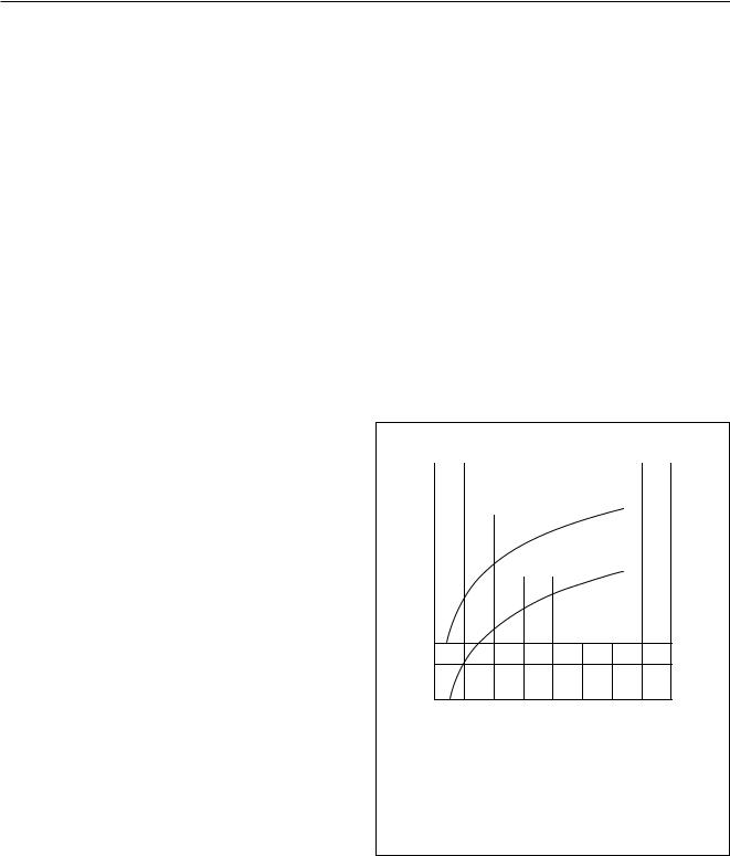
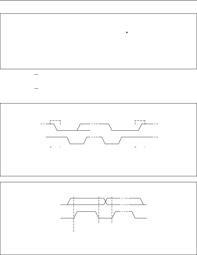
To guarantee AC-load detection, an amplifier current of more than 550 mA is required. AC-load detection will never occur with a current of less than 150 mA. Figure 3 shows which AC loads are detected at different output voltages. For example, if a load is detected at an output voltage of 2.5 V peak, the load is less than 4 Ω. If no load is detected, the output impedance is more than 14 Ω.
102 |
|
|
|
|
|
|
|
|
|
|
|
mrc331 |
|
|
|
|
|
|
|
|
|
|
|
|
|
|
|
|
|
|
|
|
|
|
|
|
|
|
|
|
|
|
|
|
|
|
|
|
|
|
|
|
|
|
|
|
|
|
|
|
|
|
|
|
|
|
no load present |
|
|
|
|
(1) |
|
|
|||
Zo(load) |
|
|
|
|
|
|
||||||
|
|
|
|
|
|
|
|
|
|
|||
|
|
|
|
|
|
|
|
|
||||
(Ω) |
|
|
|
|
|
|
|
|
|
|
|
|
|
|
|
|
|
|
|
|
|
|
|
||
|
|
|
|
|
|
|
|
|
|
|
|
|
|
|
|
|
|
|
|
|
|
|
|
|
|
10 |
|
undefined |
|
(2) |
|
|
||||||
|
|
|
|
|
|
|
|
|
|
|
|
|
|
|
|
|
|
|
|
|
|
|
|
|
|
|
|
|
|
|
|
|
|
|
|
|
|
|
|
|
|
|
|
|
|
|
|
|
|
|
|
|
|
|
|
|
|
|
|
|
|
|
|
|
|
|
|
|
|
|
|
|
|
|
|
|
|
|
|
|
|
|
|
|
|
|
|
|
|
|
load present
1
0 |
2.5 |
5 |
7.5 |
10 |
|
|
|
Vo(peak) (V) |
|
(1)IO(peak) = < 150 mA.
(2)IO(peak) = > 550 mA.
Fig.3 Tolerance of AC-load detection as a function of output voltage.
LOAD DETECTION PROCEDURE
1.At start-up, enable the ACor DC-load detection by setting D1 of instruction byte 1 to logic 1.
2004 Feb 24 |
9 |
Philips Semiconductors |
Product specification |
|
|
I2C-bus controlled 4 × 50 Watt power
TDA8588J; TDA8588xJ
amplifier and multiple voltage regulator
2.After 250 ms the DC load is detected and the mute is released. This is inaudible and can be implemented each time the IC is powered on.
3.When the amplifier start-up cycle is completed (after 1.5 s), apply an AC signal to the input, and DC-load bits D5 of each data byte should be read and stored by the microcontroller.
4.After at least 3 periods of the input signal, the load status can be checked by reading AC-detect bits D4 of each data byte.
The AC-load peak current counter can be reset by setting bit D1 of instruction byte IB1 to logic 0 and then to logic 1. Note that this will also reset the DC-load detection bits D5 in each data byte.
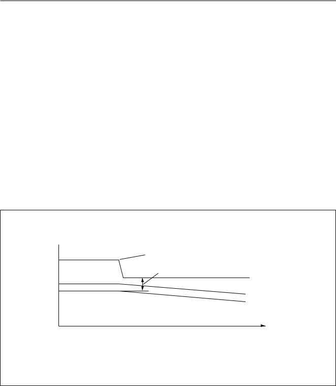
Low headroom protection
The normal DC output voltage of the amplifier is set to half the supply voltage and is related to the voltage on
pin SVR. An external capacitor is connected to pin SVR to suppress power supply ripple. If the supply voltage drops (at vehicle engine start), the DC output voltage will follow slowly due to the affect of the SVR capacitor.
The headroom voltage is the voltage required for correct operation of the amplifier and is defined as the voltage difference between the level of the DC output voltage before the VP voltage drop and the level of VP after the voltage drop (see Fig.4).
At a certain supply voltage drop, the headroom voltage will be insufficient for correct operation of the amplifier. To prevent unwanted audible noises at the output, the headroom protection mode will be activated (see Fig.4). This protection discharges the capacitors connected to pins SVR and ACGND to increase the headroom voltage.
V |
|
(V) |
vehicle engine start |
14 |
VP |
|
|
|
headroom voltage |
8.4 |
SVR voltage |
|
|
7 |
|
|
amplifier |
|
DC output voltage |
t (sec)
mdb515
Fig.4 Amplifier output during supply voltage.
2004 Feb 24 |
10 |
Philips Semiconductors |
Product specification |
|
|
I2C-bus controlled 4 × 50 Watt power
TDA8588J; TDA8588xJ
amplifier and multiple voltage regulator
VOLTAGE REGULATORS
The voltage regulator section contains:
•Four switchable regulators and one permanent active regulator
•Two power switches with loss-of-ground protection
•Reset push-pull output
•Backup functionality.
The quiescent current condition has a very low current level of 150 µA typical with only regulator 2 active. The TDA8588 uses low dropout voltage regulators for use in low voltage applications.
All of the voltage regulators except for the standby regulator can be controlled via the I2C-bus. The voltage regulator section of this device has two power switches which are capable of delivering unregulated 400 mA continuous current, and has several fail-safe protection modes. It conforms to peak transient tests and protects against continuous high voltage (24 V), short-circuits and thermal stress. A reset warning signal is asserted if regulator 2 is out of regulation. Regulator 2 will try to maintain output for as long as possible even if a thermal shut-down or any other fault condition occurs. During overvoltage stress conditions, all outputs except regulator 2 will switch off and the device will be able to supply a minimum current for an indefinite amount of time sufficient for powering the memory of a microcontroller. Provision is made for an external reserve supply capacitor to be connected to pin BUCAP which can store enough energy to allow regulator 2 to supply a microcontroller for a period long enough for it to prepare for a loss-of-voltage.
Regulator 2
Regulator 2 is intended to supply the microcontroller and has a low quiescent current. This supply cannot be shut down in response to overvoltage stress conditions, and is not I2C-bus controllable to prevent the microcontroller from being damaged by overvoltage which could occur during a disturbance of the I2C-bus. This supply will not shut down during load dump transients or during a high thermal-protection condition.
Backup capacitor
The backup capacitor is used as a backup supply for the regulator 2 output when the battery supply voltage (VP) cannot support the regulator 2 voltage.
Backup function
The backup function is implemented by a switch function, which behaves like an ideal diode between pins VP
and BUCAP; the forward voltage of this ideal diode depends on the current flowing through it. The backup function supplies regulator 2 during brief periods when no supply voltage is present on pin VP. It requires an external capacitor to be connected to pin BUCAP and ground. When the supply voltage is present on pin VP this capacitor will be charged to a level of VP − 0.3 V. When the supply voltage is absent from pin VP, this charge can then
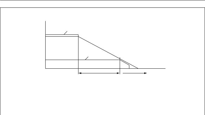
be used to supply regulator 2 for a brief period (tbackup) calculated using the formula:
tbackup |
= Cbackup |
× RL |
VP –(VO(REG2) –0.5) |
||
× |
--------------------------------------------------------V O ( REG2 ) |
|
|||
|
|
|
|
|
|
Example: VP = 14.4 V, VO(REG2) = 5 V, RL = 1 kΩ and Cbackup = 100 µF provides a tbackup of 177 ms.
When an overvoltage condition occurs, the voltage on pin BUCAP is limited to approximately 24 V; see Fig.5.
2004 Feb 24 |
11 |
Philips Semiconductors |
Product specification |
|
|
I2C-bus controlled 4 × 50 Watt power
TDA8588J; TDA8588xJ
amplifier and multiple voltage regulator
V |
|
(V) |
|
VP |
|
VBUCAP |
|
VO(REG2) |
|
|
t (sec) |
tbackup |
out of regulation |
|
mdb512 |
tbackup = Cbackup |
VP –VO(REG2) –0.5 |
|
||
|
----------------------------------------------------I L |
|
|
|
|
|
|
|
|
|
|
|
Fig.5 |
Backup capacitor function. |
|
|
|
|
|
Reset output |
|
|
|
Power switches |
A reset pulse is generated at pin RST when the output voltage of regulator 2 rises above the reset threshold value. The reset output is a push-pull output that both sources and sinks current. The output voltage can switch
between ground and VO(REG2), and operates at a low regulator 2 voltage or VBUCAP. The RST signal is controlled
by a low-voltage detection circuit which, when activated,
pulls pin RST LOW (reset active) when VO(REG2) is
≤ Vth(rst). If VO(REG2) ≥ Vth(rst), pin RST goes HIGH. The reset pulse is delayed by 40 s internally. To extend the
delay and to prevent oscillations occurring at the threshold voltage, an external capacitor can be connected to
pin RESCAP. Note that a reset pulse is not generated when VO(REG2) falls below the reset threshold value.
Reset delay capacitor
A Reset Delay Capacitor (RDC) connected to
pin RESCAP can be used to extend the delay period of the reset pulse and to ensure that a clean reset signal is sent to the microcontroller. The RDC is charged by a current source. The reset output (pin RST) will be released
(pin RST goes HIGH) when the RDC voltage crosses the RDC threshold value.
There are two power switches that provide an unregulated DC voltage output for amplifiers and an aerial motor respectively. The switches have internal protection for over-temperature conditions and are activated by setting bits D2 and D3 of instruction byte IB1 to logic 1. The regulated outputs will supply pulsed current loads that can contaminate the line with high frequency noise, so it is important to prevent any cross-coupling between the regulated outputs, particularly with the 8.3 V audio supply, and the unregulated outputs.
In the ON state, the switches have a low impedance to the battery voltage. When the battery voltage is higher than 22 V, the switches are switched off. When the battery voltage is below 22 V the switches are set to their original condition.
2004 Feb 24 |
12 |
Philips Semiconductors |
Product specification |
|
|
I2C-bus controlled 4 × 50 Watt power
TDA8588J; TDA8588xJ
amplifier and multiple voltage regulator
Protection
All regulator and switch outputs are fully protected by foldback current limiting against load dumps and short-circuits; see Fig.6. During a load dump all regulator outputs, except the output of regulator 2, will go low.
The power switches can withstand ‘loss-of-ground’. This means that if pin GND becomes disconnected, the switch is protected by automatically connecting its outputs to ground.
Temperature protection
If the junction temperature of a regulator becomes too high, the amplifier(s) are switched off to prevent unwanted noise signals being audible. A regulator junction temperature that is too high is indicated by pin DIAG going LOW and is also indicated by setting bit D6 in data byte 2.
If the junction temperature of the regulator continues to rise and reaches the maximum temperature protection level, all regulators and switches will be disabled except regulator 2.
VO(REGn) 
Isc |
Ilimit |
IO(REGn) |
|
|
MDB513 |
Fig.6 Foldback current protection.
2004 Feb 24 |
13 |
Philips Semiconductors |
Product specification |
|
|
I2C-bus controlled 4 × 50 Watt power
TDA8588J; TDA8588xJ
amplifier and multiple voltage regulator
I2C-BUS SPECIFICATION
|
|
|
|
|
|
0 |
= write |
||||
|
|
|
|
|
|
1 |
= read |
||||
MSB |
|
|
|
|
|
|
|
|
|
||
|
|
|
|
|
|
|
LSB |
||||
1 |
1 |
0 |
1 |
1 |
0 |
0 |
|
|
|
|
|
|
R/W |
|
|
||||||||
|
|
|
|
|
|
|
|
|
|
|
|
|
|
|
|
|
|
MDB516 |
|||||
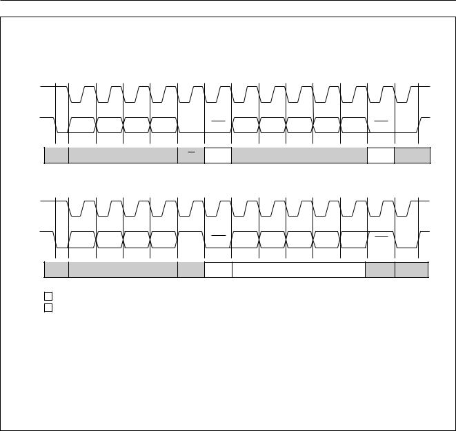
Fig.7 Address byte.
If address byte bit R/W = 0, the TDA8588 expects 3 instruction bytes: IB1, IB2 and IB3; see Table 1 to Table 6. After a power-on, all instruction bits are set to zero.
If address byte bit R/W = 1, the TDA8588 will send 4 data bytes to the microcontroller: DB1, DB2, DB3 and DB4; see Table 7 to Table 10.
SDA |
|
|
|
|
|
|
|
|
|
|
|
|
|
|
|
|
|
|
|
|
|
|
|
|
SDA |
|
|
|
|
|
|
|
|
|
|
|
|||||||||||||||
SCL |
|
|
|
S |
|
|
|
|
|
|
|
|
|
|
|
|
P |
|
SCL |
||||||
|
|
|
|
|
|
|
|
|
|
|
|
|
|
|
|
||||||||||
|
|
|
|
|
|
|
|
|
|
|
|
|
|
|
|
||||||||||
|
|
|
|
|
|
|
|
|
|
|
|
|
|
|
|
||||||||||
|
|
|
|
|
|
|
|
|
|
|
|
|
|
|
|
||||||||||
|
|
|
|
|
|
|
|
|
|
|
|
|
|
|
|
||||||||||
|
|
|
|
|
|
|
|
|
|
|
|
|
|
|
|
||||||||||
|
|
|
|
|
|
|
|
|
|
|
|||||||||||||||
|
|
|
|
|
|
|
|
|
|
|
|||||||||||||||
|
|
|
|
|
|
|
|
|
|
|
|
|
|
|
|
|
|
||||||||
|
|
|
|
|
|
|
|
|
|
|
|||||||||||||||
|
|
|
|
|
|
|
|
|
|
|
|
|
|
|
|
|
|
|
|
|
|
|
|
||
START condition |
|
|
|
|
|
|
|
STOP condition |
|||||||||||||||||
|
|
|
|
|
|
|
|
|
|
|
|
|
|
|
|
|
|
|
|
|
|
|
|
|
MBA608 |
Fig.8 Definition of start and stop conditions.
SDA
SCL
data line |
|
change |
|
|
|
|
|
||
stable; |
|
of data |
|
|
|
|
|
||
data valid |
|
allowed |
|
MBA607 |
|
|
|||
|
|
Fig.9 Bit transfer.
2004 Feb 24 |
14 |
Philips Semiconductors |
Product specification |
|
|
I2C-bus controlled 4 × 50 Watt power
TDA8588J; TDA8588xJ
amplifier and multiple voltage regulator
|
I2C-WRITE |
|
|
|
|
|
|
|
|
|
SCL |
1 |
2 |
7 |
8 |
9 |
1 |
2 |
7 |
8 |
9 |
|
||||||||||
SDA |
MSB |
MSB − 1 |
LSB + 1 |
|
ACK |
MSB |
MSB − 1 |
LSB + 1 |
LSB |
ACK |
S |
ADDRESS |
W |
A |
WRITE DATA |
A |
P |
To stop the transfer, after the last acknowledge (A) a stop condition (P) must be generated
I2C-READ |
|
|
|
|
|
|
|
|
|
|
|
SCL |
1 |
2 |
7 |
8 |
9 |
1 |
2 |
7 |
8 |
9 |
|
SDA |
MSB |
MSB − 1 |
LSB + 1 |
|
ACK |
MSB |
MSB − 1 |
LSB + 1 |
LSB |
ACK |
|
S |
|
ADDRESS |
R |
|
A |
|
READ DATA |
|
A |
P |
|
|
|
|
|
: generated by master (microcontroller) |
||
|
|
|
|
: generated by slave (TDA8588) |
||
|
S |
: start |
||||
|
P |
: stop |
||||
|
A |
: acknowledge |
||||
|
|
: read / |
|
|
||
R/W |
write |
|||||
To stop the transfer, the last byte must not be acknowledged and a stop condition (P) must be generated
mce641
Fig.10 I2C-bus read and write modes.
2004 Feb 24 |
15 |

Philips Semiconductors |
Product specification |
|
|
I2C-bus controlled 4 × 50 Watt power
TDA8588J; TDA8588xJ
amplifier and multiple voltage regulator
Table 1 Instruction byte IB1
BIT |
|
|
|
DESCRIPTION |
||||||
|
|
|
|
|
||||||
D7 |
regulator 5 output voltage control |
|||||||||
|
(see Table 2) |
|
|
|
|
|
|
|||
D6 |
|
|
|
|
|
|
||||
|
|
|
|
|
|
|
|
|
|
|
|
|
|
|
|
|
|
|
|
|
|
D5 |
|
|
|
|
|
|
|
|
|
|
|
|
|
|
|
|
|
|
|
|
|
D4 |
|
|
|
|
|
|
|
|
|
|
|
|
|
|
|
|
|
|
|
|
|
D3 |
SW2 control |
|
|
|
|
|
|
|
||
|
0 |
= SW2 off |
|
|
|
|
|
|
||
|
1 |
= SW2 on |
|
|
|
|
|
|
||
|
|
|
|
|
|
|
|
|
|
|
D2 |
SW1 control |
|
|
|
|
|
|
|
||
|
0 |
= SW1 off |
|
|
|
|
|
|
||
|
1 |
= SW1 on |
|
|
|
|
|
|
||
|
|
|
|
|
||||||
D1 |
ACor DC-load detection switch |
|||||||||
|
0 |
= ACor DC-load detection off; resets |
||||||||
|
DC-load detection bits and AC-load |
|||||||||
|
detection peak current counter |
|||||||||
|
|
|
|
|
|
|||||
|
1 |
= ACor DC-load detection on |
||||||||
|
|
|
|
|
||||||
D0 |
amplifier start enable (clear power-on reset |
|||||||||
|
flag; D7 of DB2) |
|
|
|
|
|
|
|||
|
0 |
= amplifier OFF; pin |
|
|
remains LOW |
|||||
|
DIAG |
|||||||||
|
1 |
= amplifier ON; when power-on occurs, |
||||||||
|
bit D7 of DB2 is reset and pin |
|
is |
|||||||
|
DIAG |
|||||||||
|
released |
|
|
|
|
|
|
|
||
|
|
|
|
|
||||||
Table 2 Regulator 5 (display) output voltage control |
||||||||||
|
|
|
|
|
|
|
|
|
|
|
|
|
BIT |
|
|
|
|
OUTPUT (V) |
|||
|
|
|
|
|
|
|
|
|||
D7 |
D6 |
|
D5 |
D4 |
|
|||||
|
|
|
|
|
||||||
|
|
|
|
|
|
|
|
|||
0 |
|
0 |
|
0 |
0 |
|
0 (off) |
|||
|
|
|
|
|
|
|
|
|
||
0 |
|
0 |
|
0 |
1 |
|
6.0 |
|
||
|
|
|
|
|
|
|
|
|
||
0 |
|
0 |
|
1 |
0 |
|
7.0 |
|
||
|
|
|
|
|
|
|
|
|
||
0 |
|
0 |
|
1 |
1 |
|
8.2 |
|
||
|
|
|
|
|
|
|
|
|
||
0 |
|
1 |
|
0 |
0 |
|
9.0 |
|
||
|
|
|
|
|
|
|
|
|
||
0 |
|
1 |
|
0 |
1 |
|
9.5 |
|
||
|
|
|
|
|
|
|
|
|
||
0 |
|
1 |
|
1 |
0 |
|
10.0 |
|
||
|
|
|
|
|
|
|
|
|
||
0 |
|
1 |
|
1 |
1 |
|
10.4 |
|
||
|
|
|
|
|
|
|
|
|
||
1 |
|
0 |
|
0 |
0 |
|
12.5 |
|
||
|
|
|
|
|
|
|
|
|||
1 |
|
0 |
|
0 |
1 |
|
≤ VP − 1 |
|||
|
|
|
|
|
|
|
|
(switch) |
||
|
|
|
|
|
|
|
|
|
|
|
Table 3 Instruction byte IB2
BIT |
|
DESCRIPTION |
|
|
|
||
D7 |
regulator 4 output voltage control (see |
||
|
Table 4) |
||
D6 |
|||
|
|
||
|
|
|
|
D5 |
|
|
|
|
|
||
D4 |
regulator 3 (mechanical digital) control |
||
|
0 |
= regulator 3 off |
|
|
1 |
= regulator 3 on |
|
|
|
||
D3 |
regulator 1 output voltage control (see |
||
|
Table 5) |
||
D2 |
|||
|
|
||
|
|
||
D1 |
soft mute all amplifier channels (mute delay |
||
|
20 ms) |
||
|
0 |
= mute off |
|
|
1 |
= mute on |
|
|
|
||
D0 |
hard mute all amplifier channels (mute delay |
||
|
0.4 ms) |
||
|
0 |
= mute off |
|
|
1 |
= mute on |
|
|
|
|
|
Table 4 Regulator 4 (mechanical drive) output voltage control
|
BIT |
|
OUTPUT (V) |
|
|
|
|
||
D7 |
D6 |
D5 |
||
|
||||
|
|
|
|
|
0 |
0 |
0 |
0 (off) |
|
|
|
|
|
|
0 |
0 |
1 |
5 |
|
|
|
|
|
|
0 |
1 |
0 |
6 |
|
|
|
|
|
|
0 |
1 |
1 |
7 |
|
|
|
|
|
|
1 |
0 |
0 |
8.6 |
|
|
|
|
|
Table 5 Regulator 1 (audio) output voltage control
|
BIT |
OUTPUT (V) |
|
|
|
|
|
D3 |
|
D2 |
|
|
|
||
|
|
|
|
0 |
|
0 |
0 (off) |
|
|
|
|
0 |
|
1 |
8.3 |
|
|
|
|
1 |
|
0 |
8.5 |
|
|
|
|
1 |
|
1 |
8.7 |
|
|
|
|
2004 Feb 24 |
16 |

Philips Semiconductors |
Product specification |
|
|
I2C-bus controlled 4 × 50 Watt power
TDA8588J; TDA8588xJ
amplifier and multiple voltage regulator
Table 6 Instruction byte IB3
|
BIT |
|
DESCRIPTION |
|
|
|
|
D7 |
|
clip detection level |
|
|
|
0 |
= 4 % detection level |
|
|
1 |
= 1 % detection level |
|
|
|
|
D6 |
|
amplifier channels 1 and 2 gain select |
|
|
|
0 |
= 26 dB gain (normal mode) |
|
|
1 |
= 20 dB gain (line driver mode) |
|
|
|
|
D5 |
|
amplifier channels 3 and 4 gain select |
|
|
|
0 |
= 26 dB gain (normal mode) |
|
|
1 |
= 20 dB gain (line driver mode) |
|
|
|
|
D4 |
|
amplifier thermal protection pre-warning |
|
|
|
0 |
= warning at 145 °C |
|
|
1 |
= warning at 122 °C |
|
|
|
|
D3 |
|
disable channel 1 |
|
|
|
0 |
= enable channel 1 |
|
|
1 |
= disable channel 1 |
|
|
|
|
D2 |
|
disable channel 2 |
|
|
|
0 |
= enable channel 2 |
|
|
1 |
= disable channel 2 |
|
|
|
|
D1 |
|
disable channel 3 |
|
|
|
0 |
= enable channel 3 |
|
|
1 |
= disable channel 3 |
|
|
|
|
D0 |
|
disable channel 4 |
|
|
|
0 |
= enable channel 4 |
|
|
1 |
= disable channel 4 |
|
|
|
|
Table 7 Data byte DB1
BIT |
|
DESCRIPTION |
|
|
|
D7 |
amplifier thermal protection pre-warning |
|
|
0 |
= no warning |
|
1 |
= junction temperature above pre-warning |
|
level |
|
|
|
|
D6 |
amplifier maximum thermal protection |
|
|
0 |
= junction temperature below 175 °C |
|
1 |
= junction temperature above 175 °C |
|
|
|
D5 |
channel 4 DC load detection |
|
|
0 |
= DC load detected |
|
1 |
= no DC load detected |
|
|
|
D4 |
channel 4 AC load detection |
|
|
0 |
= no AC load detected |
|
1 |
= AC load detected |
|
|
|
D3 |
channel 4 load short-circuit |
|
|
0 |
= normal load |
|
1 |
= short-circuit load |
|
|
|
D2 |
channel 4 output offset |
|
|
0 |
= no output offset |
|
1 |
= output offset |
|
|
|
D1 |
channel 4 VP short-circuit |
|
|
0 |
= no short-circuit to VP |
|
1 |
= short-circuit to VP |
D0 |
channel 4 ground short-circuit |
|
|
0 |
= no short-circuit to ground |
|
1 |
= short-circuit to ground |
|
|
|
2004 Feb 24 |
17 |
Loading...