Philips (Now NXP) TDA6107AJF Schematic [ru]

TDA6107AJF
Triple video output amplifier
Rev. 02 — 28 April 2005 Product data sheet
1. General description
The TDA6107AJF contains three video output amplifiers which are intended to drive the
three cathodes of a color CRT. The device is contained in a plastic DIL-bent-SIL 9-pin
medium power (DBS9MPF) package, and uses high-voltage DMOS technology.
To obtain maximum performance, the amplifier should be used with black-current control.
2. Features
■ Typical bandwidth of 5.5 MHz for an output signal of 60 V (p-p)
■ High slew rate of 900 V/µs
■ No external components required
■ Very simple application
■ Single supply voltage of 200 V
■ Internal reference voltage of 2.5 V
■ Fixed gain of 81
■ Black-Current Stabilization (BCS) circuit with voltage window from 1.8 V to 6 V and
current window from +100 µA to −10 mA
■ Thermal protection
■ Internal protection against positive flashover discharges appearing on the CRT
3. Ordering information
Table 1: Ordering information
Type number Package
Name Description Version
TDA6107AJF DBS9MPF plastic DIL-bent-SIL medium power package with fin; 9 leads SOT111-1

Philips Semiconductors
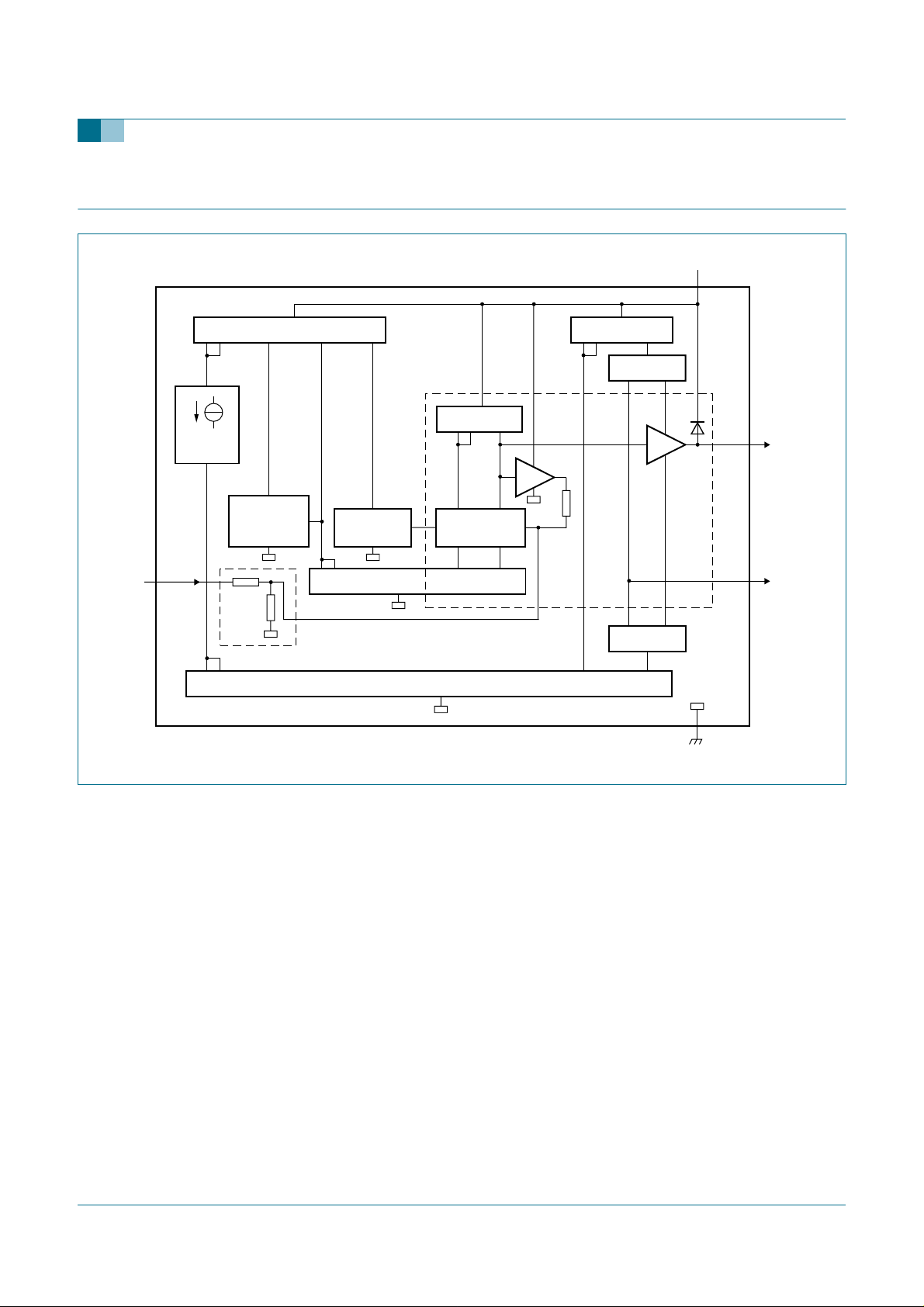
4. Block diagram
TDA6107AJF
Triple video output amplifier
V
DD
6
MIRROR 1
CURRENT
SOURCE
THERMAL
PROTECTION
CIRCUIT
V
,
i(1)
1, 2, 3
V
,
i(2)
V
i(3)
R
i
R
a
VIP
REFERENCE
MIRROR 3
3×
Fig 1. Block diagram (one amplifier shown)
TDA6107AJF
MIRROR 4
DIFFERENTIAL
MIRROR 2
STAGE
MIRROR 5
CASCODE 1
3×
V
,
1×
1×
R
f
CASCODE 2
9, 8, 7
4
mce457
oc(1)
V
,
oc(2)
V
oc(3)
5
I
om
9397 750 14728 © Koninklijke Philips Electronics N.V. 2005. All rights reserved.
Product data sheet Rev. 02 — 28 April 2005 2 of 16

Philips Semiconductors
5. Pinning information
5.1 Pinning
GND
V
V
V
V
i(1)
V
i(2)
V
i(3)
I
om
V
DD
oc(3)
oc(2)
oc(1)
1
2
3
4
5
TDA6107AJF
6
7
8
9
001aac587
TDA6107AJF
Triple video output amplifier
Fig 2. Pin configuration
5.2 Pin description
Table 2: Pin description
Symbol Pin Description
V
i(1)
V
i(2)
V
i(3)
GND 4 ground (fin)
I
om
V
DD
V
oc(3)
V
oc(2)
V
oc(1)
1 inverting input 1
2 inverting input 2
3 inverting input 3
5 black-current measurement output
6 supply voltage
7 cathode output 3
8 cathode output 2
9 cathode output 1
9397 750 14728 © Koninklijke Philips Electronics N.V. 2005. All rights reserved.
Product data sheet Rev. 02 — 28 April 2005 3 of 16

Philips Semiconductors
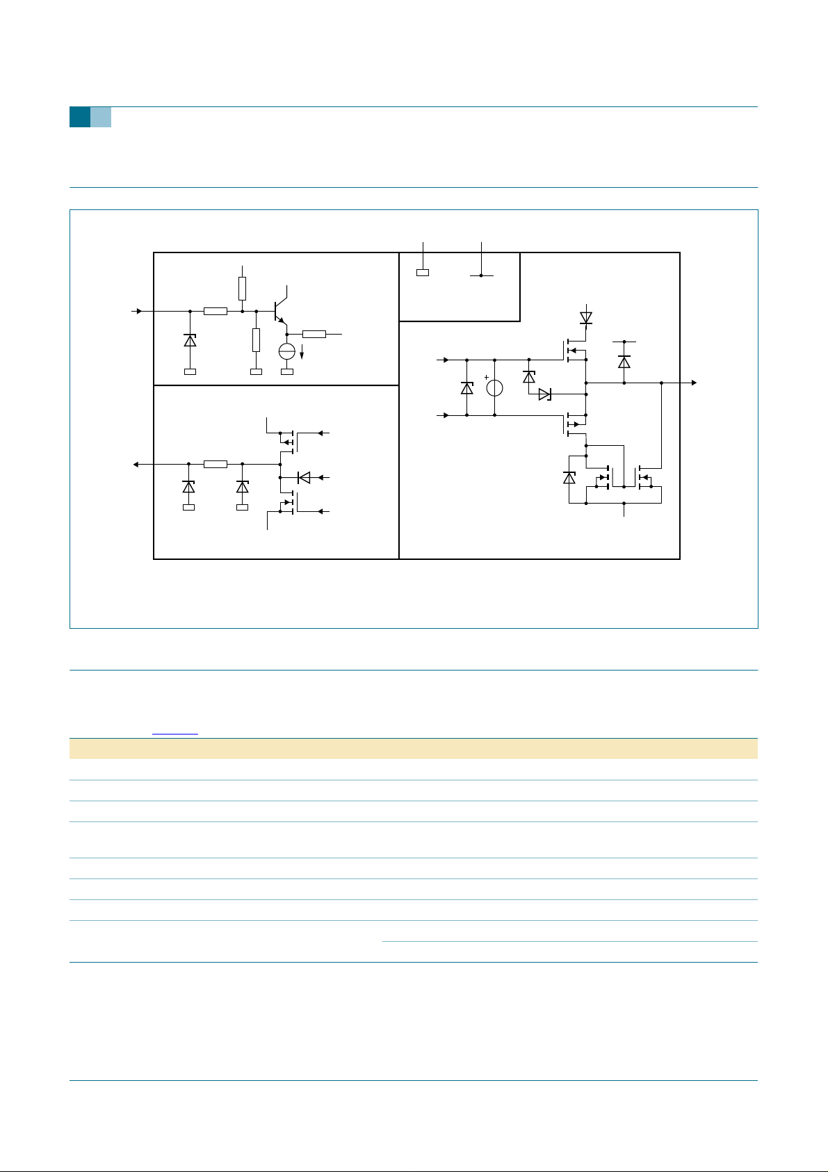
6. Internal circuitry
GND
TDA6107AJF
Triple video output amplifier
V
DD
46
TDA6107AJF
from
input
circuit
from
input
circuit
1, 2, 3
5
esd
to black-current
measurement circuit
6.8 Vesd
to black-current
measurement circuit
to cascode
stage
from
control
circuit
from blackcurrent
measurement
circuit
from
control
circuit
(1) All pins have an energy protection for positive or negative overstress situations.
Fig 3. Internal pin configuration
7. Limiting values
esd
to black-current
measurement circuit
(1)
flash
7, 8, 9
mce458
V
bias
esd
esd
esd
measurement circuit
to black-current
Table 3: Limiting values
In accordance with the Absolute Maximum Rating System (IEC 60134). Voltages measured with respect to ground; currents
as specified in
Figure 9; unless otherwise specified.
Symbol Parameter Conditions Min Max Unit
V
DD
V
i
V
om
|I
om(mean)
V
oc
T
stg
T
j
V
esd
supply voltage 0 250 V
input voltage at pins V
i(1),Vi(2)
and V
i(3)
012V
measurement output voltage 0 6 V
| absolute value of mean current of
measurement output (for three channels)
cathode output voltage 0 V
Voc=0VtoVDD;
V
=1.8Vto6V
om
- 5.6 mA
DD
storage temperature −55 +150 °C
junction temperature −20 +150 °C
electrostatic discharge voltage Human Body Model (HBM) - ±3000 V
V
Machine Model (MM) - ±300 V
9397 750 14728 © Koninklijke Philips Electronics N.V. 2005. All rights reserved.
Product data sheet Rev. 02 — 28 April 2005 4 of 16

Philips Semiconductors
8. Thermal characteristics
Table 4: Thermal characteristics
Symbol Parameter Conditions Typ Unit
R
th(j-a)
R
th(j-fin)
[1] An external heatsink is necessary; see
thermal resistance from junction to ambient in free air 56 K/W
thermal resistance from junction to fin
Application Note AN10227-01
TDA6107AJF
Triple video output amplifier
[1]
11 K/W
.
mbh989
T
amb
(°C)
(1) Infinite heatsink.
(2) No heatsink.
8
P
tot
(W)
6
4
2
0
−40 0 40 80 160120
(1)
(2)
Fig 4. Power derating curves
8.1 Thermal protection
The internal thermal protection circuit gives a decrease of the slew rate at high
temperatures: 10 % decrease at 130 °C and 30 % decrease at 145 °C (typical values on
the spot of the thermal protection circuit).
outputs
5 K/W
thermal protection circuit
6 K/W
fin
mgk279
Fig 5. Equivalent thermal resistance network
9397 750 14728 © Koninklijke Philips Electronics N.V. 2005. All rights reserved.
Product data sheet Rev. 02 — 28 April 2005 5 of 16

Philips Semiconductors
TDA6107AJF
Triple video output amplifier
9. Characteristics
Table 5: Characteristics
Operating range: Tj=−20°C to +150°C; VDD= 180 V to 210 V; test conditions: T
V
oc(1)=Voc(2)=Voc(3)
test circuit of
Figure 9; unless otherwise specified.
1
=
⁄
2VDD;CL
=10pF(CLconsists of parasitic and cathode capacitance); R
Symbol Parameter Conditions Min Typ Max Unit
I
q
V
ref(int)
quiescent supply current 5.6 6 7.6 mA
internal reference voltage (input
stage)
R
i
input resistance - 2.1 - kΩ
G gain of amplifier 73 81 89
∆G gain difference −4.2 0 +4.2
PSRR power supply rejection ratio f < 50 kHz
α
ct(DC)
Measurement output pin I
I
om(offset)
/∆I
∆I
om
oc
Output pins V
V
oc(DC)
∆V
oc(DC)(offset)
DC crosstalk between channels - −50 - dB
; Voc=V
om
offset current of measurement
output (for three channels)
linearity of current transfer
(for three channels)
, V
oc(2)
, V
oc(3)
oc(1)
oc(min)
to V
oc(max)
Ioc=0µA;
V
=1.8Vto6V
om
Ioc= −100 µA to +100 µA;
V
=1.8Vto6V
om
= −100 µA to +10 mA;
I
oc
V
=1.8Vto4V
om
DC output voltage Ii=0µA 76 8797V
differential DC output offset
Ii=0µA −5 0 +5 V
voltage between two output pins
∆V
oc(T)
∆V
oc(T)(offset)
output voltage temperature drift - 10 - mV/K
differential output offset voltage
temperature drift between two
output pins
I
oc(max)
V
oc(min)
V
oc(max)
B
S
B
L
t
co(p)
∆t
co(p)
maximum peak output current Voc=50VtoVDD− 50 V - 20 - mA
minimum output voltage Vi= 4.5 V; at Ioc=0mA
maximum output voltage Vi= 0.5 V; at Ioc=0mA
small signal bandwidth Voc= 60 V (p-p) - 5.5 - MHz
large signal bandwidth Voc= 100 V (p-p) - 4.5 - MHz
cathodeoutputpropagationtime
50 % input to 50 % output
difference in cathode output
propagation time 50 % input to
Voc= 100 V (p-p) square
wave
V
= 100 V (p-p) square
oc
wave
50 % output (between two
output pins)
t
oc(r)
t
oc(f)
cathode output rise time
10 % output to 90 % output
cathode output fall time
90 % output to 10 % output
Voc= 50 V to 150 Vsquare
wave
Voc= 150 V to 50 Vsquare
wave
=25°C; VDD= 200 V;
amb
= 18 K/W; measured in
th(h-a)
- 2.5 - V
[1]
-55-dB
−50 - +50 µA
−0.9 −1.0 −1.1
−0.9 −1.0 −1.1
- 0 - mV/K
[2]
- - 10 V
[2]
VDD− 15--V
[3]
-60-ns
[3]
−10 0 +10 ns
[3]
67 91 113 ns
[3]
67 91 113 ns
9397 750 14728 © Koninklijke Philips Electronics N.V. 2005. All rights reserved.
Product data sheet Rev. 02 — 28 April 2005 6 of 16
 Loading...