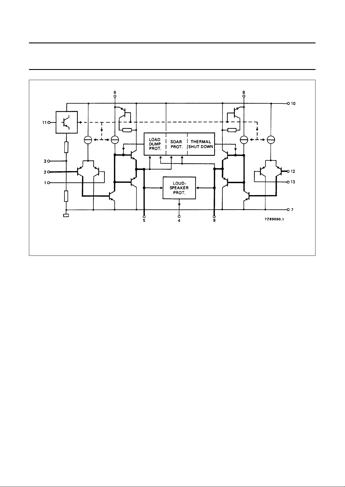
Philips (Now NXP) TDA1515BQ Schematic [ru]

INTEGRATED CIRCUITS
DATA SH EET
TDA1515BQ
24 W BTL or 2 x 12 W stereo
car radio power amplifier
Product specification
File under Integrated Circuits, IC01
July 1994

Philips Semiconductors Product specification
24 W BTL or 2 x 12 W stereo
TDA1515BQ
car radio power amplifier
The TDA1515BQ is a monolithic integrated class-B output amplifier in a 13-lead single in-line (SIL) plastic power
package. The device is primarily developed for car radio applications, and also to drive low-impedance loads (down to
1,6 Ω). At a supply voltage VP= 14,4 V, an output power of 24 W can be delivered into a 4 Ω BTL (Bridge Tied Load),
or, when used as stereo amplifier, it delivers 2 × 12 W into 2 Ω or 2 × 7 W into 4 Ω.
Special features are:
• flexibility in use − mono BTL as well as stereo
• high output power
• low offset voltage at the output (important for BTL)
• large usable gain variation
• very good ripple rejection
• internal limited bandwidth for high frequencies
• low stand-by current possibility (typ. 1 µA), to simplify required switches; TTL drive possible
• low number and small sized external components
• high reliability.
The following currently required protections are incorporated in the circuit. These protections also have positive influence
on reliability in the applications.
• load dump protection
• a.c. and d.c. short-circuit safe to ground up to VP= 18 V
• thermal protection
• speaker protection in bridge configuration
• SOAR protection
• outputs short-circuit safe to ground in BTL
• reverse polarity safe.
July 1994 2

Philips Semiconductors Product specification
24 W BTL or 2 x 12 W stereo
car radio power amplifier
QUICK REFERENCE DATA
Supply voltage range (operating) V
Supply voltage (non-operating) V
Supply voltage (non-operating; load dump protection) V
Repetitive peak output current I
Total quiescent current I
Stand-by current I
Switch-on current I
Input impedance |Z
Bridge tied load application (BTL) V
Output power at R
= 0,5% P
d
tot
= 10% P
d
tot
Supply voltage ripple rejection; R
D.C. output offset voltage between the outputs |∆V
= 4 Ω (with bootstrap)
L
= 0 Ω; f = 100 Hz RR typ. 50 50 dB
S
TDA1515BQ
P
P
P
ORM
tot
sb
so
|> 1MΩ
i
P
o
o
| < 50 50 mV
5-9
max. 28 V
max. 45 V
max. 4 A
typ. 75 mA
typ. 1 µA
< 100 µA
= 14,4 13,2 V
typ. 18 15 W
typ. 24 20 W
6 to 18 V
Stereo application
Output power at d
= 4 Ω P
R
L
= 2 Ω P
R
L
Output power at d
= 4 Ω P
R
L
R
= 2 Ω P
L
= 10% (with bootstrap)
tot
= 0,5% (with bootstrap)
tot
o
o
o
o
typ. 7 6 W
typ. 12 10 W
typ. 5,5 4,5 W
typ. 9 7,5 W
Channel separation α >40 40dB
Noise output voltage; R
= 10 kΩ; according to IEC curve-A V
S
n
typ. 0,2 0,2 mV
PACKAGE OUTLINE
13-lead SIL-bent-to-DIL; plastic power (SOT141C); SOT141-6; 1996 July 19.
July 1994 3

Philips Semiconductors Product specification
24 W BTL or 2 x 12 W stereo
car radio power amplifier
TDA1515BQ
Fig.1 Internal block diagram; the heavy lines indicate the signal paths.
RATINGS
Limiting values in accordance with the Absolute Maximum System (IEC 134)
Supply voltage; operating (pin 10) V
Supply voltage; non-operating V
Supply voltage; during 50 ms (load dump protection) V
Peak output current I
Total power dissipation see derating curve Fig.2
Storage temperature range T
Crystal temperature T
A.C. and d.c. short-circuit safe voltage max. 18 V
Reverse polarity max. 10 V
P
P
P
OM
stg
c
max. 18 V
max. 28 V
max. 45 V
max. 6 A
−55 to + 150 °C
max. 150 °C
July 1994 4
 Loading...