SAA7130HL
PCI video broadcast decoder
Rev. 04 — 11 April 2006 Product data sheet
1. General description
The SAA7130HL is a single chip solution to digitize and decode video, and capture it
through the PCI-bus.
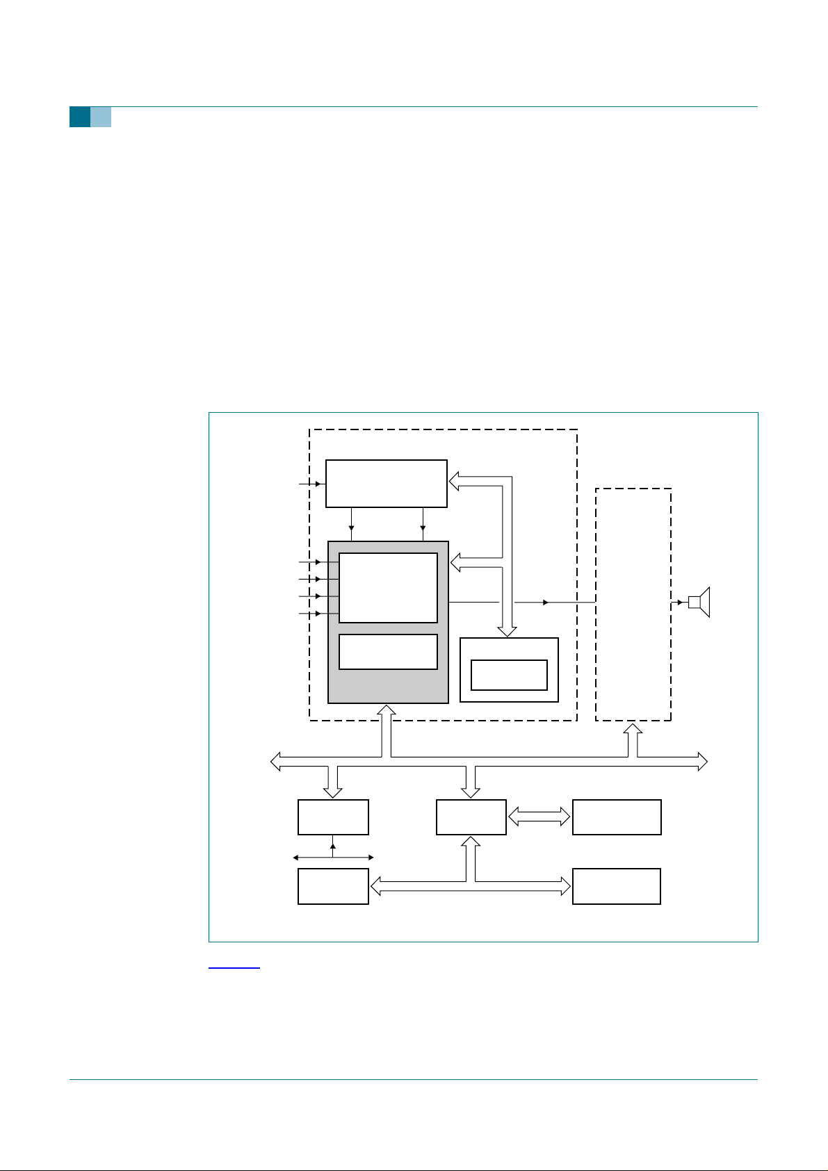
Special means are incorporated to maintain the synchronization of audio to video. The
device offers versatile peripheral interfaces (GPIO) that support various extended
applications, e.g. analog audio pass-through for loopback cable to the sound card, or
capture of DTV and DVB transport streams, such as Vestigial Side Band (VSB),
Orthogonal Frequency Division Multiplexing (OFDM) and Quadrature Amplitude
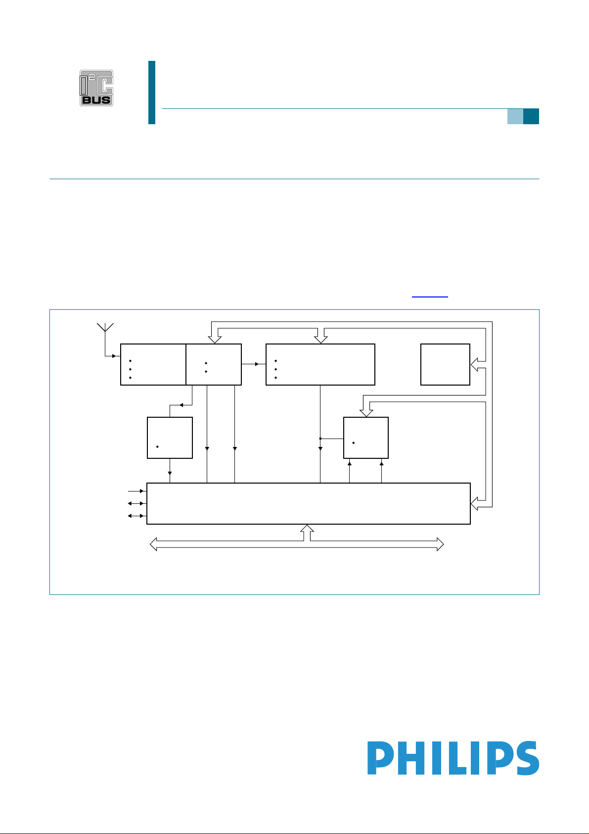
Modulation (QAM) decoded digital television standards, see Figure 1.
I2C-bus
CVBS
S-video
audio I/O
line-in
line-out
TV TUNER:
CABLE
TERRESTRIAL
SATELLITE
AUDIO
DECODER:
BTSC
audio
L/R
IF-PLL:
DVB
ATV
SIF
CVBS
AF
(mono)
DECODER FOR TV VIDEO
WITH TS INTERFACE AND
DMA MASTER INTO PCI-BUS
DIGITAL CHANNEL DECODER:
DTV
VSB
QAM
DVB
OFDM
PCI-bus
TS
ENCODER:
MPEG2
2
I
S-bus ITU656
SAA7130HL
2
I
C-BUS
EEPROM
mhc169
Fig 1. Application diagram for capturing live TV video in the PC, with optional extensions for enhanced DTV and
DVB capture
1.1 Introduction
The PCI video broadcast decoder SAA7130HL is a highly integrated, low cost and solid
foundation for TV capture in the PC, for analog TV and digital video broadcast. The
various multimedia data types are transported over the PCI-bus by bus-master-write, to
optimally exploit the streaming capabilities of a modern host-based system. Legacy
requirements are also taken care of.

Philips Semiconductors
SAA7130HL
PCI video broadcast decoder
The SAA7130HL meets the requirements of
PC design guides 98/99 and 2001
PCI 2.2 and Advanced Configuration and Power Interface (ACPI) compliant.
The analog video is sampled by 9-bit ADCs, decoded by a multi-line adaptive comb filter
and scaled horizontally, vertically and by field rate.Multiplevideooutputformats(YUVand
RGB) are available, including packed and planar, gamma-compensated or
black-stretched.
Audio is routed as an analog signal via the loopback cable to the sound card.
The SAA7130HL provides a versatile peripheral interface to support system extensions,
e.g. MPEG encoding for time-shift viewing, or DSP applications for audio enhancements.
The channel decoder for digital video broadcast reception (ATSC or DVB) can re-use the
integrated video ADCs.
The Transport Stream (TS) is collected by a tailored interface and pumped through the
PCI-bus to the system memory in well-defined buffer structures. Various internal events,
or peripheral status information, can be enabled as an interrupt on the PCI-bus.
1.2 Overview of TV decoders with PCI bridge
A TV decoder family with PCI interfacing has been created to support worldwide
TV broadcasting. The pin compatibility of these TV decoders offers the opportunity to
support different TV broadcast standards with one PCB layout.
and is
Table 1: TV decoder family with PCI interfacing
TV parameter TV decoder type
SAA7130HL SAA7133HL SAA7134HL SAA7135HL
PCI bridge version 2.2 2.2 2.2 2.2
DMA channel 7777
TV video
decoding
Video
scaling
Raw VBI 27 MHz sampling rate XXXX
TV sound
decoding
Radio FM radio stereo - X - X
PAL, NTSC and
SECAM
2 dimension and
2 task scaler
FM A2 and NICAM - - X X
BTSC (dbx-TV) plus
SAP; EIAJ
stereo sampling
2
S-bus and DMA)
(I
XXXX
XXXX
-X-X
- 32 kHz 32 kHz,
[1]
48 kHz
32 kHz,
48 kHz
SAA7130HL_4 © Koninklijke Philips Electronics N.V. 2006. All rights reserved.
Product data sheet Rev. 04 — 11 April 2006 2 of 46

Philips Semiconductors
SAA7130HL
PCI video broadcast decoder
Table 1: TV decoder family with PCI interfacing
TV parameter TV decoder type
SAA7130HL SAA7133HL SAA7134HL SAA7135HL
Audio left and right
pass-through
stereo sampling
2
(I
S-bus and DMA)
video frame locked
audio
incredible surround - X X X
volume, bass and
treble control
Transport
stream
GPIO static I/O pins 27 27 27 27
[1] X = function available.
serial and parallel TS XXXX
interrupt input pins 4444
2
C-bus multi-master
I
or slave
video out XXXX
XXXX
- 32 kHz,
- XXX
- X volume only X
XXXX
…continued
[1]
44.1 kHz,
48 kHz
32 kHz,
44.1 kHz,
48 kHz
32 kHz,
44.1 kHz,
48 kHz
1.3 Related documents
This document describes the functionality and characteristics of the SAA7130HL.
Other documents related to the SAA7130HL are:
•
User manual SAA7130HL/34HL
•
Application note SAA7130HL/34HL
, describing the programmability
, pointing out recommendations for system
implementation
• Demonstration and reference boards, including description, schematics, etc.:
– Proteus-Pro: TV capture PCI card for analog TV (standards: B/G, I, D/K and L/L’)
– Europe: hybrid DVB-Tand analog TV capture PCI card for European broadcasting.
• Data sheets of other devices referred to in this document, e.g:
–
TDA8961
–
TD1316
–
TDA10045
–
TDA9886
–
TDA9889
: DTV channel decoder
: ATV+DVB-T tuner
: DVB channel receiver
: analog IF-PLL
: digital IF-PLL
SAA7130HL_4 © Koninklijke Philips Electronics N.V. 2006. All rights reserved.
Product data sheet Rev. 04 — 11 April 2006 3 of 46

Philips Semiconductors
2. Features
2.1 PCI and DMA bus mastering
■ PCI 2.2 compliant including full Advanced Configuration and Power Interface (ACPI)
■ System vendor ID, etc. via EEPROM
■ Hardware support for virtual addressing by MMU
■ DMA bus master write for video, VBI and TS
■ Configurable PCI FIFOs, graceful overflow
■ Packed and planar video formats, overlay clipping
2.2 TV video decoder and video scaling
■ All-standards TV decoder: NTSC, PAL and SECAM
■ Five analog video inputs: CVBS and S-video
■ Video digitizing by two 9-bit ADCs at 27 MHz
■ Sampling according
■ Adaptive comb filter for NTSC and PAL, also operating for non-standard signals
■ Automatic TV standard detection
■ Three level Macrovision copy protection detection according to Macrovision detect
specification revision 1
■ Control of brightness, contrast, saturation and hue
■ Versatile filter bandwidth selection
■ Horizontal and vertical downscaling or zoom
■ Adaptive anti-alias filtering
■ Capture of raw VBI samples
■ Two alternating settings for active video scaling
■ Output in YUV and RGB
■ Gamma compensation, black stretching
ITU-R BT.601
SAA7130HL
PCI video broadcast decoder
with 720 pixels/line
2.3 TV audio I/O
■ Integrated analog audio pass-through for analog audio loopback cable to sound card
2.4 Peripheral interface
■ I2C-bus master interface: 3.3 Vand 5 V
■ Digital video output: ITU and VIP formats
■ TS input: serial or parallel
■ General purpose I/O, e.g. for strapping and interrupt
■ Propagate reset and ACPI state D3-hot
2.5 General
■ Package: LQFP128
■ Power supply: 3.3 V only
■ Power consumption of typical application: 1 W
■ Standby state (D3-hot): < 0.02 W
SAA7130HL_4 © Koninklijke Philips Electronics N.V. 2006. All rights reserved.
Product data sheet Rev. 04 — 11 April 2006 4 of 46
Philips Semiconductors
■ All interface signals 5 V tolerant
■ Reference designs available
■ SDK for Windows (98, 2000 and XP) and Windows Driver Model (WDM)
3. Ordering information
Table 2: Ordering information
Type
number
SAA7130HL LQFP128 plastic low profile quad flat package; 128 leads;
4. Block diagram
SAA7130HL
PCI video broadcast decoder
Package
Name Description Version
SOT425-1
body 14 × 20 × 1.4 mm
base-
band
audio
inputs
CVBS
S-video
inputs
digital
data
inputs
left 1
right 1
left 2
right 2
CV0
CV1
CV2
CV3
CV4
TS data
TS data
2
S-bus
I
GPIO
interrupt
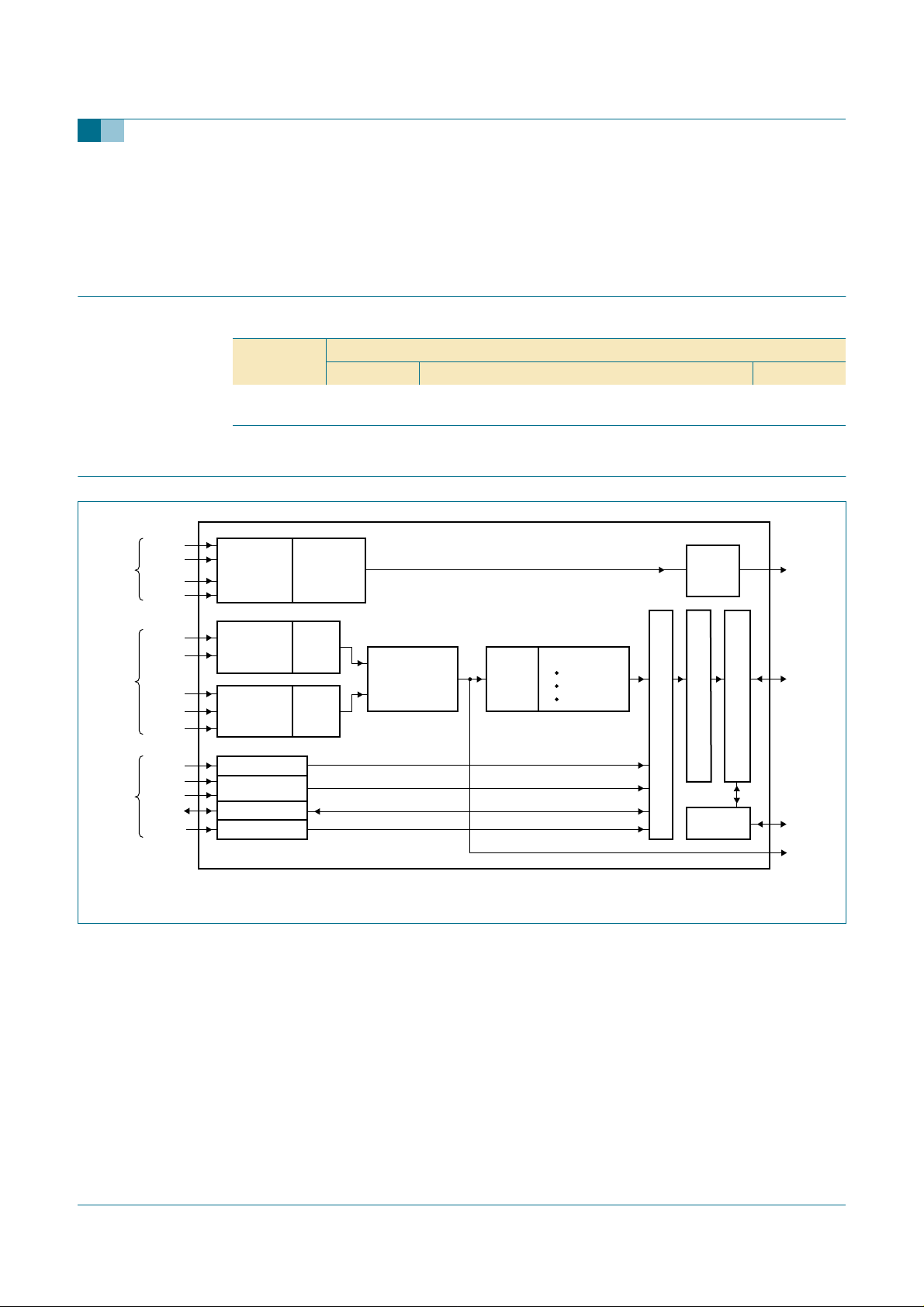
Fig 2. Block diagram
ANALOG
NF/AUDIO
FRONT-END
ANALOG
VIDEO
FRONT-END
ANALOG
VIDEO
FRONT-END
TS PARALLEL
TS SERIAL
STATIC I/O
IRQ
STEREO
BUFFER
9-BIT
VIDEO
ADC
9-BIT
VIDEO
ADC
DIGITAL VIDEO
COMB FILTER
DECODER
SAA7130HL
VIDEO
SCALER
PIXEL ENGINE:
MATRIX
GAMMA
FORMAT
FIFO
AUDIO
OUTPUT
DMA
REGISTER
UNIT
audio
stereo
output
PCI-bus
PCI INTERFACE
2
I
C-bus
ITU656
mhc170
SAA7130HL_4 © Koninklijke Philips Electronics N.V. 2006. All rights reserved.
Product data sheet Rev. 04 — 11 April 2006 5 of 46
Philips Semiconductors
5. Pinning information
5.1 Pinning
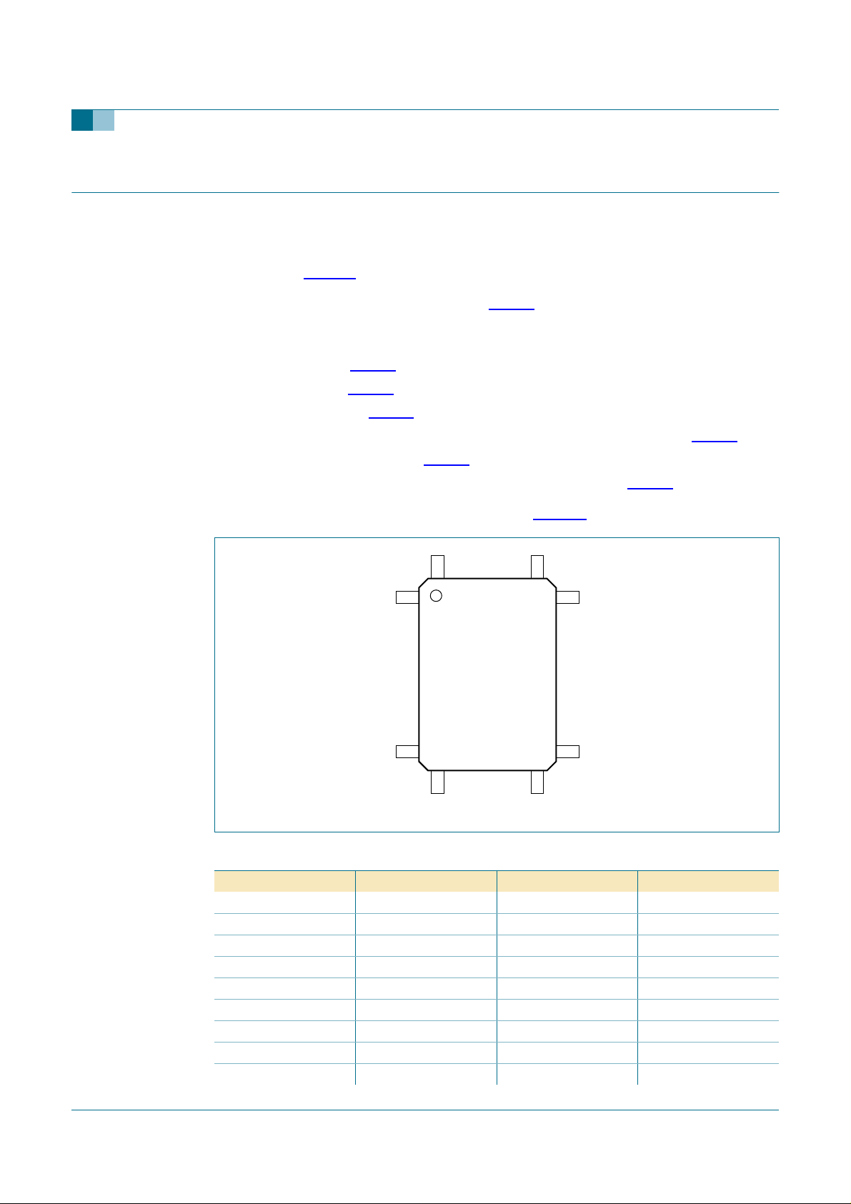
The SAA7130HL is packaged in a rectangular Low profile Quad Flat Package (LQFP) with
128 pins, see Figure 3.
All the pins are shown sorted by number in Table 3.
Functional pin groupings are given in the following tables:
Power supply pins: Table 4
PCI interface pins: Table 5
Analog interface pins: Table 6
Joint Test Action Group (JTAG) test interface pins for boundary scan test: Table 7
I2C-bus multi-master interface: Table 8
General purpose interface (pins GPIO) and the main functions: Table 9
SAA7130HL
PCI video broadcast decoder
The characteristics of the pin types are detailed in Table 10.
128
1
SAA7130HL
38
39
Fig 3. Pin configuration
Table 3: Pin allocation table
Pin Symbol Pin Symbol Pin Symbol Pin Symbol
1V
DDD
33 C/BE[1]# 65 V
2 GNT# 34 AD[15] 66 V_CLK 98 RIGHT1
3 REQ# 35 AD[14] 67 GPIO17 99 V
4 AD[31] 36 AD[13] 68 GPIO16 100 RIGHT2
5 AD[30] 37 AD[12] 69 GPIO15 101 n.c.
6 AD[29] 38 V
7 AD[28] 39 V
DDD
SSD
8 AD[27] 40 PCI_CLK 72 GPIO12 104 OUT_LEFT
9 AD[26] 41 AD[11] 73 V
103
102
65
64
001aac204
DDD
97 V
SSA
REF0
70 GPIO14 102 n.c.
71 GPIO13 103 OUT_RIGHT
DDD
105 PROP_RST_N
SAA7130HL_4 © Koninklijke Philips Electronics N.V. 2006. All rights reserved.
Product data sheet Rev. 04 — 11 April 2006 6 of 46

Philips Semiconductors
SAA7130HL
PCI video broadcast decoder
Table 3: Pin allocation table
…continued
Pin Symbol Pin Symbol Pin Symbol Pin Symbol
10 AD[25] 42 AD[10] 74 V
SSD
11 AD[24] 43 AD[09] 75 GPIO11 107 V
12 C/BE[3]# 44 AD[08] 76 GPIO10 108 V
106 n.c.
REF3
SSA
13 IDSEL 45 C/BE[0]# 77 GPIO9 109 CV2_C
14 AD[23] 46 AD[07] 78 GPIO8 110 V
DDA
15 AD[22] 47 AD[06] 79 GPIO7 111 n.c.
16 AD[21] 48 AD[05] 80 GPIO6 112 DRCV_Y
17 AD[20] 49 AD[04] 81 GPIO5 113 V
SSA
18 AD[19] 50 AD[03] 82 GPIO4 114 CV0_Y
19 V
20 V
DDD
SSD
51 AD[02] 83 GPIO3 115 V
DDA
52 AD[01] 84 GPIO2 116 CV1_Y
21 AD[18] 53 AD[00] 85 GPIO1 117 DRCV_C
22 AD[17] 54 V
23 AD[16] 55 V
DDD
SSD
86 GPIO0 118 CV3_C
87 GPIO27 119 V
SSA
24 C/BE[2]# 56 GPIO23 88 GPIO26 120 CV4
25 FRAME# 57 GPIO22 89 GPIO25 121 TRST_N
26 IRDY# 58 GPIO21 90 SCL 122 TCK
27 TRDY# 59 GPIO20 91 SDA 123 TMS
28 DEVSEL# 60 GPIO19 92 V
29 STOP# 61 GPIO18 93 V
DDD
SSD
124 TDO
125 TDI
30 PERR# 62 XTALI 94 LEFT2 126 INT_A
31 SERR# 63 XTALO 95 V
32 PAR 64 V
SSD
96 LEFT1 128 V
DDA
127 PCI_RST#
SSD
5.2 Pin description
Table 4: Power supply pins
Symbol Pin Type Description
V
SSA
97, 108,
113
and 119
V
DDA
95, 110
and 115
V
SSD
20, 39, 55,
64, 74, 93
and 128
V
DDD
1, 19, 38,
54, 65, 73
and 92
SAA7130HL_4 © Koninklijke Philips Electronics N.V. 2006. All rights reserved.
Product data sheet Rev. 04 — 11 April 2006 7 of 46
AG analog ground for integrated analog signal processing
AS analog supply voltage for integrated analog signal
processing
VG digital ground for digital circuit, core and input/outputs
VS digital supply voltage for digital circuit, core and
input/outputs

Philips Semiconductors
SAA7130HL
PCI video broadcast decoder
Table 5: PCI interface pins
Symbol Pin Type Description
PCI_CLK 40 PI PCI clock input: reference for all bus transactions, up to
PCI_RST# 127 PI PCI reset input: will 3-state all PCI pins (active LOW)
AD[31] to
AD[00]
C/BE[3]# to
C/BE[0]#
PAR 32 PIO and
FRAME# 25 PIO and
TRDY# 27 PIO and
IRDY# 26 PIO and
STOP# 29 PIO and
IDSEL 13 PI initialization device select input: this input is used to
DEVSEL# 28 PIO and
REQ# 3 PO PCI request output: the SAA7130HL requests master
GNT# 2 PI PCI grant input: the SAA7130HL is granted to master
INT_A 126 PO and
PERR# 30 PIO and
SERR# 31 PO and
4 to 11,
14 to 18,
21 to 23,
34 to 37,
41 to 44
and
46 to 53
12, 24, 33
and 45
[1]
PIO and
T/S
PIO and
T/S
T/S
S/T/S
S/T/S
S/T/S
S/T/S
S/T/S
O/D
S/T/S
O/D
33.33 MHz
multiplexed address and data input or output:
bidirectional, 3-state
command code input or output: indicates type of
requested transaction and byte enable, for byte aligned
transactions (active LOW)
parity input or output: driven by the data source, even
parity over all pins AD and C/BE#
frame input or output: driven by the current bus master
(owner), to indicate the beginning and duration of a bus
transaction (active LOW)
target ready input or output: driven by the addressed
target, to indicate readiness for requested transaction
(active LOW)
initiator ready input or output: driven by the initiator, to
indicate readiness to continue transaction (active LOW)
stop input or output: target is requesting the master to
stop the current transaction (active LOW)
select the SAA7130HL during configuration read and
write transactions
device selectinputoroutput: drivenby the target device,
to acknowledge address decoding (active LOW)
access to PCI-bus (active LOW)
access PCI-bus (active LOW)
interrupt A output: this pin is an open-drain interrupt
output, conditions assigned by the interrupt register
parity error input or output: the receiving device detects
data parity error (active LOW)
system error output: reports address parity error (active
LOW)
[1] PCI-bus pins are located on the long side of the package to simplify PCI board layout requirements.
Table 6: Analog interface pins
Symbol Pin Type Description
XTALI 62 CI quartz oscillator input: 32.11 MHz or 24.576 MHz
XTALO 63 CO quartz oscillator output
LEFT2 94 AI analog audio stereo left 2 input or mono input
SAA7130HL_4 © Koninklijke Philips Electronics N.V. 2006. All rights reserved.
Product data sheet Rev. 04 — 11 April 2006 8 of 46
[1]

Philips Semiconductors
SAA7130HL
PCI video broadcast decoder
Table 6: Analog interface pins
…continued
[1]
Symbol Pin Type Description
V
DDA
95 AS analog supply voltage (3.3 V)
LEFT1 96 AI analog audio stereo left 1 input or mono input; default
analog pass-through to pin OUT_LEFT after reset
V
SSA
97 AG analog ground (for audio)
RIGHT1 98 AI analog audio stereo right 1 input or mono input; default
analog pass-through to pin OUT_RIGHT after reset
V
REF0
99 AR analog reference ground for audio Sigma Delta ADC; to be
connected directly to analog ground (V
SSA
)
RIGHT2 100 AI analog audio stereo right 2 input or mono input
n.c. 101 - not connected
n.c. 102 - not connected
OUT_RIGHT 103 AO analog audio stereo right channel output; 1 V (RMS)
line-out, feeding the audio loopback cable via a coupling
capacitor of 2.2 µF
OUT_LEFT 104 AO analog audio stereo left channel output; 1 V (RMS) line-out,
feeding the audio loopback cable via a coupling capacitor of
2.2 µF
PROP_RST_N 105 AO analog output for test and debug purposes (active LOW)
n.c. 106 - not connected
V
REF3
107 AR analog reference voltage for audio FIR-DAC and SCART
audio input buffer; to be supported with two parallel
capacitors of 47 µF and 0.1 µF to analog ground (V
V
SSA
108 AG analog ground
SSA
)
CV2_C 109 AI composite video input (mode 2) or C input (modes 6 and 8)
V
DDA
110 AS analog power supply (3.3 V)
n.c. 111 - not connected
DRCV_Y 112 AR differential reference connection (for CV0 and CV1); to be
supported with a capacitor of 47 nF to analog ground (V
V
SSA
113 AG analog ground
SSA
CV0_Y 114 AI composite video input (mode 0) or Y input (modes 6 and 8)
V
DDA
115 AS analog supply voltage (3.3 V)
CV1_Y 116 AI composite video input (mode 1) or Y input (modes 7 and 9)
DRCV_C 117 AR differential reference connection (forCV2,CV3and CV4); to
be supported with a capacitor of 47 nF to analog ground
)
(V
SSA
CV3_C 118 AI composite video input (mode 3) or C input (modes 7 and 9)
V
SSA
119 AG analog ground
CV4 120 AI composite video input (mode 4)
)
[1] The SAA7130HL offers an interfacefor analog video and audiosignals. The related analog supply pinsare
included in this table.
SAA7130HL_4 © Koninklijke Philips Electronics N.V. 2006. All rights reserved.
Product data sheet Rev. 04 — 11 April 2006 9 of 46

Philips Semiconductors
Table 7: JTAG test interface pins
Symbol Pin Type Description
TRST_N 121 I test reset input: drive LOW for normal operating (active
TCK 122 I test clock input: drive LOW for normal operating
TMS 123 I test mode select input: tie HIGH or let float for normal
TDO 124 O test serial data output: 3-state
TDI 125 I test serial data input: tie HIGH or let float for normal
Table 8: I
Symbol Pin Type Description
SCL 90 IO2 serial clock input (slave mode) or output (multi-master
SDA 91 IO2 serial data input and output; always available
PROP_RST_N 105 GO propagate reset and D3-hot output; to peripheral board
LOW)
operating
operating
2
C-bus multi-master interface
mode)
circuitry
SAA7130HL
PCI video broadcast decoder
Table 9: GPIO pins and functions
Symbol Pin Type Function
GPIO27 87 GIO ---R/W
GPIO26 88 GIO ---R/W
GPIO25 89 GIO ---R/W
V_CLK 66 GO V_CLK (also
GPIO23 56 GIO HSYNC - ADC_C[0] (LSB) R/W,
GPIO22 57 GIO VSYNC TS_LOCK
GPIO21 58 GIO - TS_S_D
GPIO20 59 GIO - TS_CLK
GPIO19 60 GIO - TS_SOP (packet
GPIO18 61 GIO VAUX2 - X_CLK_IN R/W,
GPIO17 67 GIO VAUX1 (e.g.
[1]
Audio and
video port
outputs
gated)
VACTIVE)
TS capture
inputs
- ADC_CLK (out) -
(channel
decoder locked)
(bit-serial data)
(< 33 MHz)
start)
- ADC_Y[0] (LSB) R/W
Raw DTV/DVB
outputs
- R/W,
- R/W
- R/W
- R/W
GPIO
INT
INT
INT
SAA7130HL_4 © Koninklijke Philips Electronics N.V. 2006. All rights reserved.
Product data sheet Rev. 04 — 11 April 2006 10 of 46

Philips Semiconductors
SAA7130HL
PCI video broadcast decoder
Table 9: GPIO pins and functions
…continued
[1]
Symbol Pin Type Function
Audio and
video port
TS capture
inputs
Raw DTV/DVB
outputs
GPIO
outputs
GPIO16 68 GIO - TS_VAL (valid
flag)
GPIO15 to
GPIO8
69 to 72
and
75 to 78
GIO VP[7:0] for
formats:
ITU-R BT.656
- ADC_Y[8:1] R/W
,
- R/W,
INT
VMI, VIP (1.1,
2.0), etc.
GPIO7 to
GPIO0
79 to 86 GIO VP extension
for 16-bit
formats: ZV,
TS_P_D[7:0]
(byte-parallel
data)
ADC_C[8:1] R/W
VIP-2, DMSD,
etc.
[1] The SAA7130HL offers a peripheral interface with General Purpose Input/Output (GPIO) pins. Dedicated
functions can be selected:
a) Digital Video Port (VP): output only; in 8-bit and 16-bit formats, such as VMI, DMSD (
zoom-video,with discrete sync signals;
EAV codes.
b) Transport Stream (TS) capture input: from the peripheral DTV/DVB channel decoder; synchronized by
Start Of Packet (SOP); in byte-parallel or bit-serial protocol.
c) Digitized raw DTV/DVB samples stream output: from internal ADCs; to feed the peripheral DTV/DVB
channel decoder.
d) GPIO: as default (no other function selected); static (no clock); read and write from or to individually
selectable pins; latching ‘strap’ information at system reset time.
e) Use an external pull-up resistor of 4.7 kΩ at GPIO16 for an external 24.576 MHz crystal; due to an
internal pull-down resistor an open GPIO16 pin requires an external 32.11 MHz crystal.
f) Peripheral interrupt (INT) input: enabled by interrupt enable register; routed to PCI interrupt (INT_A).
ITU-R BT.656
; VIP (1.1and 2.0), with sync encodedin SAV and
ITU-R BT.601
);
5.2.1 Pin type description
Table 10: Characteristics of pin types and remarks
Pin type Description
AG analog ground
AI analog input; video, audio and sound
AO analog output
AR analog reference support pin
AS analog supply voltage (3.3 V)
CI CMOS input; 3.3 V level (not 5 V tolerant)
CO CMOS output; 3.3 V level (not 5 V tolerant)
GIO digital input/output (GPIO); 3.3 V level (5 V tolerant)
GO digital output (GPIO); 3.3 V level (5 V tolerant)
I JTAG test input
2
IO2 digital input and output of the I
compatible, auto-adapting
O JTAG test output
O/D open-drain output (for PCI-bus); multiple clients can drive LOW at the
same time, wired-OR, floating back to 3-state over several clock cycles
SAA7130HL_4 © Koninklijke Philips Electronics N.V. 2006. All rights reserved.
Product data sheet Rev. 04 — 11 April 2006 11 of 46
C-bus interface; 3.3 V and 5 V

Philips Semiconductors
SAA7130HL
PCI video broadcast decoder
Table 10: Characteristics of pin types and remarks
Pin type Description
PI input according to PCI-bus requirements
PIO input and output according to PCI-bus requirements
PO output according to PCI-bus requirements
S/T/S sustained 3-state (for PCI-bus); previous owner drives HIGH for one
T/S 3-state I/O (for PCI-bus); bidirectional
VG ground for digital supply
VS supply voltage (3.3 V)
Name ends with _N or # this pin or ‘signal’ isactive LOW, i.e. the function is ‘true’ ifthelogiclevel
6. Functional description
6.1 Overview of internal functions
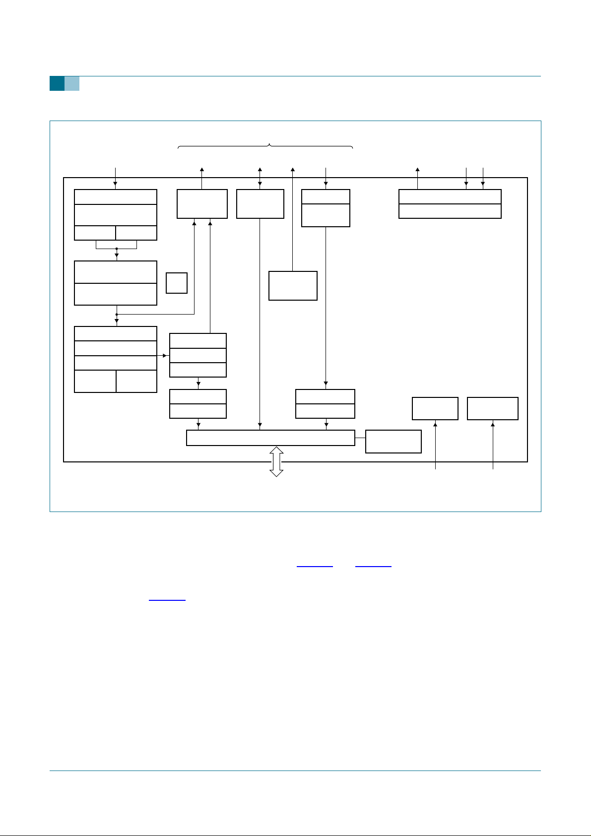
The SAA7130HL is able to capture TV signals over the PCI-bus in personal computers by
a single chip; see Figure 4.
The SAA7130HL incorporates two 9-bit video ADCs and the entire decoding circuitry for
any analog TV signal: NTSC, PAL and SECAM, including non-standard signals, such as
playback from a VCR. The adaptive multi-line comb filter provides superb picture quality,
component separation, sharpness and high bandwidth. The video stream can be cropped
and scaled to the needs of the application. Scaling down as well as zooming up is
supported in the horizontal and vertical direction, and an adaptive filter algorithm prevents
aliasing artifacts. With the acquisition unit of the scaler two different ‘tasks’ can be defined,
e.g. to capture video to the CPU for compression, and write video to the screen from the
same video source but with different resolution, color format and frame rate.
…continued
clock cycle before leaving to 3-state
is LOW
The SAA7130HL incorporates analog audio pass-through and support for the analog
audio loopback cable to the sound card function.
The decoded video streams are fed to the PCI-bus, and are also applied to a peripheral
streaming interface, in ITU, VIP or VMI format. A possible application extension is
on-board hardware MPEG compression, or other feature processing. The compressed
data is fed back through the peripheral interface,in parallelor serial format, to be captured
by the system memory through the PCI-bus. The Transport Stream (TS) from a DTV/DVB
channel decoder can be captured through the peripheral interface in the same way.
Video and transport streams are collected in a configurable FIFO with a total capacity of
1 kB. The DMA controller monitors the FIFO filling degree and master-writes the audio
and video stream to the associated DMA channel. The virtual memory address space
(from OS) is translated into physical (bus) addresses by the on-chip hardware Memory
Management Unit (MMU).
The application of the SAA7130HL is supported by reference designs and a set of drivers
for the Windows operating system (Windows driver model compliant).
SAA7130HL_4 © Koninklijke Philips Electronics N.V. 2006. All rights reserved.
Product data sheet Rev. 04 — 11 April 2006 12 of 46
Philips Semiconductors
SAA7130HL
PCI video broadcast decoder
5 analog
video
inputs
INPUT SELECTION
CLAMP AND GAIN
CONTROL
9-BIT ADC 9-BIT ADC
DECODER
(NTSC, PAL, SECAM)
ADAPTIVE
COMB FILTER
VIDEO SCALER
3-D
RAW VBI
PROGRAM
SET
PROGRAM
SET
digital video
output
VIDEO PORT
(DIGITAL)
LLC
MATRIX
GAMMA
FORMAT
VIDEO FIFOS
DMA CONTROL
GPIO
2
C-bus
I
I2C-BUS
INTERFACE
PROPAGATE
reset
RESET
DMA CONTROL
transport
stream input
DTV-TS p/s
I2S-BUS
INPUT
TS FIFOS
stereo
output
ANALOG AUDIO I/O
PASS-THROUGH (DEFAULT)
stereo
input 1
stereo
input 2
SAA7130HL
BOUNDARY
SCAN TEST
OSCILLATOR
Fig 4. Functional diagram
6.2 Application examples
The SAA7130HL enables PC TV capture applications both on the PC motherboard and
on PCI add-on TV capture cards. Figure 5 and Figure 6 illustrate some examples of
add-on card applications.
Figure 5 shows the basic application to capture video from analog TV sources. The
proposed tuner types incorporate the RF tuning function and the IF down conversion.
Usually the IF down conversion stage also includes a single channel and analog sound
FM demodulator. The Philips tuner FI1216 MK2 is dedicated to the 50 Hz system
B/G standard as used in Europe. The FI1236 MK2 is the comparable type for the 60 Hz
system M standard for the USA. Both types are suited for terrestrial broadcast and for
cable reception. The tuner provides composite video and baseband audio as mono or
‘multiplexed’ (mpx) in case of BTSC. These analog video and sound signals are fed to the
appropriate input pins of the SAA7130HL.
Further analog video input signals, CVBS and/or Y-C, can be connected via the board
back panel, or the separate front connectors, e.g. from a camcorder. Accompanying
stereo audio signals can also be fed to the SAA7130HL.
PCI-BUS INTERFACE
PCI-bus
ACPI POWER
MANAGEMENT
crystaltest
mhc171
SAA7130HL_4 © Koninklijke Philips Electronics N.V. 2006. All rights reserved.
Product data sheet Rev. 04 — 11 April 2006 13 of 46
Philips Semiconductors
Video is digitized and decoded to YUV. The digital streams are pumped via DMA into the
PCI memory space.
The SAA7130HL incorporates the means for legacy analog audio signal routing. The
analog audio input signal is fed via an analog audio loopback cable into the line-in of a
legacy sound card. An external audio signal, that would have otherwise connected directly
to the sound card, is now routed through the SAA7130HL. This analog pass-through is
enabled as default by a system reset, i.e. without any driver involvement and before
system setup.
During the power-up procedure, the SAA7130HL will investigate the on-board EEPROM
to load the board-specific system vendor ID and board version ID into the related places
of the PCI configuration space. The board vendor can store other board-specific data in
the EEPROM that is accessible via the I2C-bus.
SAA7130HL
PCI video broadcast decoder
TV CAPTURE PCI CARD
TV cable
terrestrial
CVBS
S-video
audio
line-in
or
SOUTH
BRIDGE
TV TUNER AND
IF-PLL
CVBS
DECODER FOR
TV VIDEO
DMA MASTER
INTO PCI
SAA7130HL
ISA
AF sound
(mono)
I2C-BUS EEPROM
SYSTEM
VENDOR ID
PCI-bus:
digital video, raw VBI, TS
NORTH
BRIDGE
2
I
C-bus
analog
audio
loopback
cable
AGP
SOUND
CARD
VGA AND
LOCAL MEMORY
SYSTEM
MEMORY
FSB
CPU AND
CACHE MEMORY
mhc172
Fig 5. TV mono capture card
Figure 6 shows an application extension with a hybrid TV tuner front-end and digital
terrestrial channel decoding for DVB-T.
The single-conversion tuner TD1316 provides two dedicated IF signals for the analog
IF-PLL (TDA9886) and the digital IF-PLL (TDA9889). The CVBS (video) and AUD (audio,
mono) output signals of the analog IF-PLL can be routed to one of the video inputs and
SAA7130HL_4 © Koninklijke Philips Electronics N.V. 2006. All rights reserved.
Product data sheet Rev. 04 — 11 April 2006 14 of 46
 Loading...