Philips (Now NXP) SA57000-25D, SA57000-25UK, SA57000-28D, SA57000-28UK, SA57000-29D Schematic [ru]
...
INTEGRATED CIRCUITS
SA57000-XX
CapFREE 150 mA, low-noise, low dropout
regulator with thermal protection
Product data
Supersedes data of 2003 Apr 30
2003 Jul 30

Philips Semiconductors Product data
CapFREE 150 mA, low-noise, low dropout regulator
with thermal protection
GENERAL DESCRIPTION
The CapFREE SA57000 is the first in a new family of unique low
dropout regulators. It needs no external capacitors, offers a low
output noise voltage of 30 µV
of 55 mV @ 50 mA output current. To accommodate high density
layouts, it is packaged in the small footprint 5 leaded SOT23-5 (SO5)
and a 5-bump Wafer Level Chip- Scale package (WL-CSP5). It is ideal
for all portable and cellular phone applications.
Additional features include power and thermal shutdown, output
current limitation, power OK status, thermal warning, and external
logic-controlled on-off via the PWRON pin.
FEATURES
•CapFREE: No output capacitor needed, stable for all capacitive
loads, regardless of ESR
•5 leaded SOT23-5 (SO5) and Wafer Level Chip-Scale (WL-CSP5)
packages
•Low 30 µV
noise without noise bypass capacitor
RMS
•Preset output voltages to 2.5 V, 2.8 V, 2.9 V, 3.0 V, 3.1 V, 3.3 V
and 3.6 V; other voltages available upon request. 2% output
voltage accuracy
•150 mA maximum output current with current limitation
, and an ultra-low dropout voltage
RMS
WL-CSP5 SOT23-5
•Typical dropout voltage 55 mV @ 50 mA output current
•85 µA typical ground current
•Shut-down (standby) current < 1 µA
•Thermal-overload and short-circuit protection
•PWROK pin: both power status and thermal warning indicator
•PWRON pin offers logic-controlled shutdown
•Maximum line regulation: 0.1%/V
•Maximum load regulation: 0.02%/mA.
APPLICA TIONS
•Cordless and mobile phones
•Industrial and medical equipment
•Other battery-powered equipment.
SA57000-XX
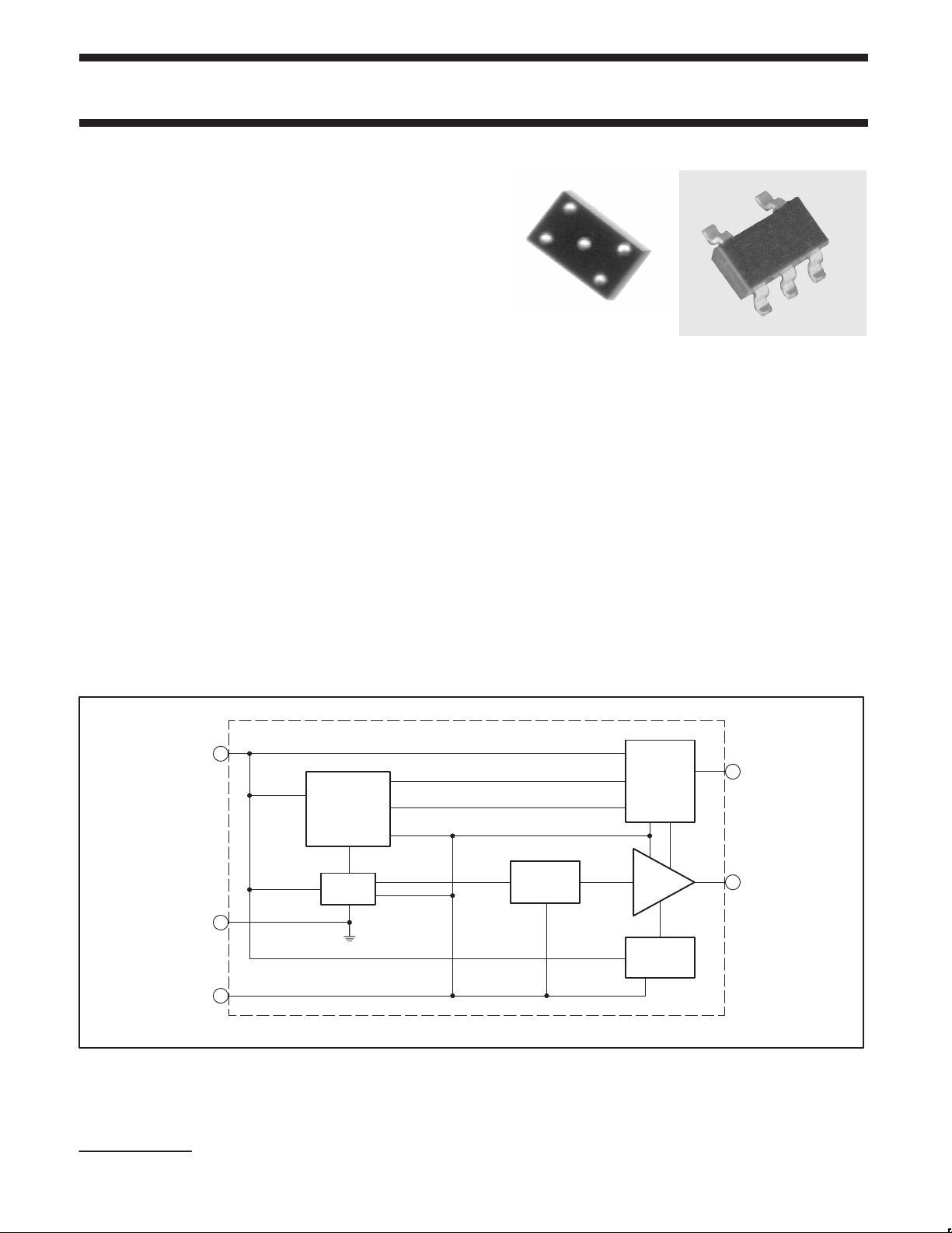
SIMPLIFIED SYSTEM DIAGRAM
GND
V
3
PWRON
PWRON
2
1
IN
PWRON
TEMPERATURE
SENSOR
BAND
GAP
Figure 1. Simplified system diagram.
SA57000
OVER 144 °C (POWER/THERMAL SHUTDOWN)
OVER 127 °C (POWER/THERMAL WARNING)
LOW-PASS
FILTER
PWRON
PWRON
LOGIC
CONTROL
OUTPUT
AMP.
BIAS
NETWORK
SA00557
4
5
PWROK
V
OUT
CapFREE is a trademark of Philips Electronics North America Corporation.
2003 Jul 30
2

Philips Semiconductors Product data
TYPE NUMBER
CapFREE 150 mA, low-noise, low dropout regulator
SA57000-XX
with thermal protection
ORDERING INFORMATION
PACKAGE
NAME DESCRIPTION VERSION
SA57000-XXD
SOT23-5,
SO5
plastic small outline package; 5 leads (see dimensional drawing) SOT680-1 –40 to +85 °C
SA57000-XXUK WL-CSP5 wafer level, chip-scale package; 5 bumps (see dimensional drawing) –40 to +85 °C
NOTE:
The device has seven voltage output options, indicated by the XX
on the Type Number.
XX
VOLTAGE (Typical)
25 2.5 V
28 2.8 V
29 2.9 V
30 3.0 V
31 3.1 V
33 3.3 V
36 3.6 V
Marking code
Each device is marked with a four letter code. The first three letters
designate the product. The fourth, represented by an ‘x’, designates
the date tracking code.
Part
SA57000-25UK, SA57000-25D ABKx
SA57000-28UK, SA57000-28D ABLx
SA57000-29UK, SA57000-29D ABXx
SA57000-30UK, SA57000-30D ABMx
SA57000-31UK, SA57000-31D ABYx
SA57000-33UK, SA57000-33D ABNx
SA57000-36UK, SA57000-36D ABPx
TEMPERATURE
RANGE
Marking
PIN CONFIGURATION
1
V
IN
2
GND
34
TOP VIEW
A3
V
OUT
V
IN
SA57000-XXUK
B2
A1
TOP VIEW
(BALLS ARE ON THE BOTTOM)
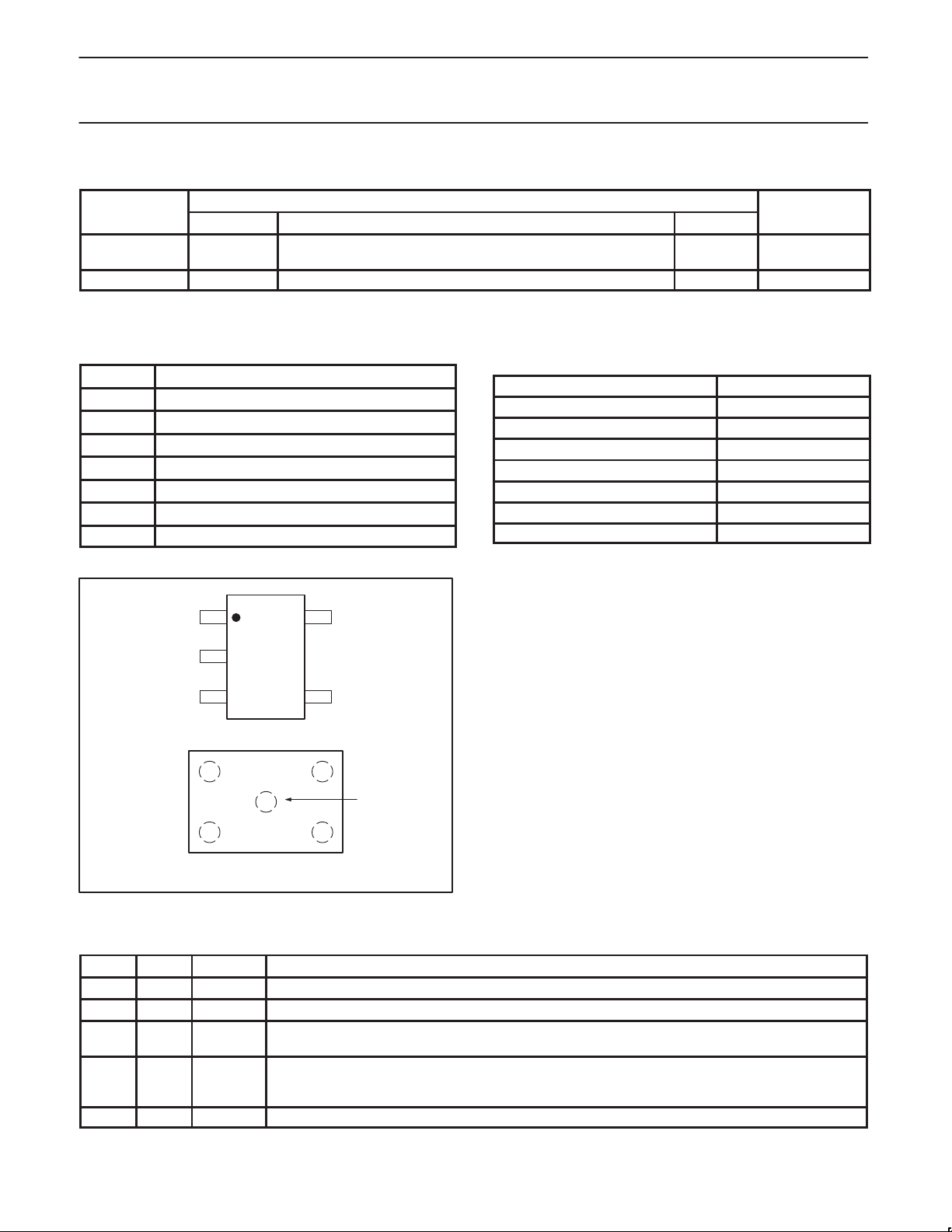
Figure 2. Pin configurations.
5V
SA57000-XXD
C3
C1
OUT
PWROKPWRON
PWROK
GND
PWRON
SA00556
PIN DESCRIPTION
PIN BALL SYMBOL DESCRIPTION
1 A1 V
IN
2 B2 GND Ground.
3 C1 PWRON Power-on input. Active-HIGH. A logic LOW powers down the regulator. The shutdown quiescent current is
4 C3 PWROK Power OK indicator, including thermal warning. Connect a 10 kΩ resistor between PWROK and V
5 A3 V
OUT
Regulator input. V
OUT(nom)
+ 0.5 V to 6.5 V. No bypass capacitor required.
typically 50 nA. Connect to VIN for manual operation.
Active-LOW open-drain output indicates an out-of-regulation condition when power falls typically 6% below
VOUT(nom), or thermal warning (trips at 127 °C ± 2 °C).
Regulator output. Sources up to 150 mA. No bypass capacitors required.
OUT
.
2003 Jul 30
3

Philips Semiconductors Product data
CapFREE 150 mA, low-noise, low dropout regulator
SA57000-XX
with thermal protection
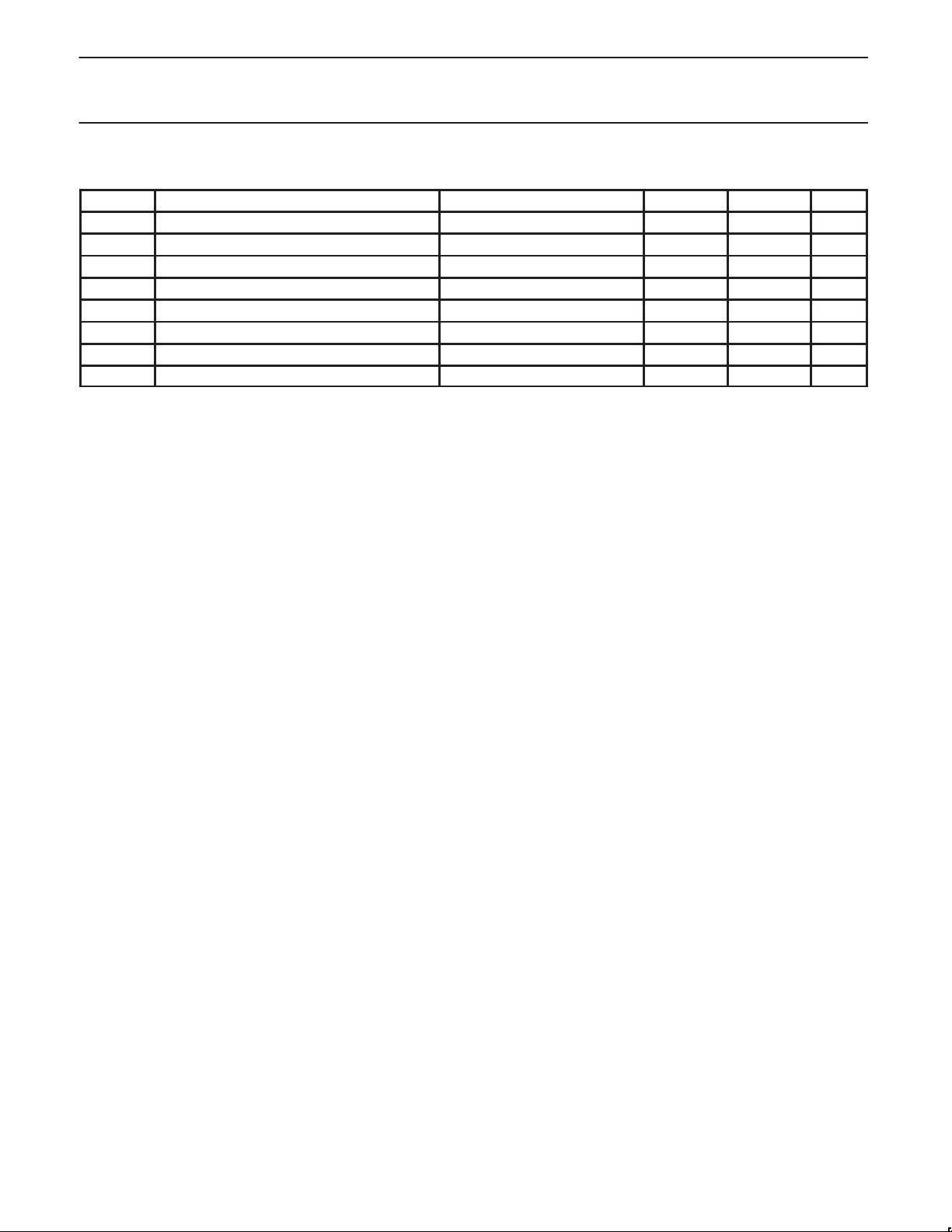
MAXIMUM RATINGS
SYMBOL PARAMETER CONDITIONS MIN. MAX. UNIT
V
IN
V
PWRON
V
OUT
T
amb
T
j
T
stg
P Power dissipation (Derating factor above 25 °C) T
R
th(j-a)
VIN to GND voltage –0.3 6.5 V
PWRON to GND voltage –0.3 6.5 V
OUT to GND voltage –0.3 VIN + 0.3 V
Operating ambient temperature –40 +85 °C
Junction temperature – +125 °C
Storage temperature –65 +160 °C
= 25 °C – 637 mW
amb
Thermal resistance from junction to ambient – 140 °C/W
DC
DC
DC
2003 Jul 30
4

Philips Semiconductors Product data
2
3
4
CapFREE 150 mA, low-noise, low dropout regulator
with thermal protection
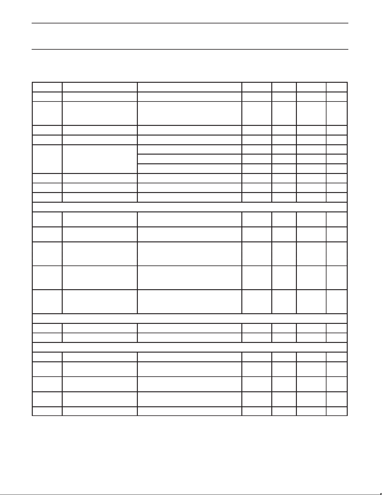
CHARACTERISTICS
VIN = V
OUT(nom)
SYMBOL
V
IN
I
LIM
I
Q
∆V
LNR
∆V
LDR
e
n
Shutdown
V
IH
V
IL
I
PWRON
I
Q(SHDN)
t
PWRON
Thermal protection (Note 2)
T
SHDN
∆T
SHDN
PWROK output (power and temperature OK) (Note 2)
NOTES:
1. Limits are production tested at T
guaranteed by design.
2. Accuracy ±2 °C over temperature range guaranteed by design and characterization.
3. The dropout voltage is defined as V
4. Time needed for V
+ 0.5 V. (Note 1.)
PARAMETER CONDITIONS MIN. TYP. MAX. UNIT
input voltage V
I
output voltage accuracy
–40 °C ≤ T
= 1 mA
OUT
T
= +25 °C – ±1 – %
amb
≤ +85 °C –2.0 – 2.0 %
amb
current limit 160 300 – mA
ground pin current I
dropout voltage
line regulation VIN = (V
load regulation I
output voltage noise f = 10 Hz to 100 kHz, C
PWRON input threshold
(HIGH ON-state)
PWRON input threshold
(HIGH ON-state)
PWRON input bias current
shutdown supply current
power-on start-up time
= 1 mA to 150 mA – 85 150 µA
OUT
I
= 1 mA – 1 – mV
OUT
I
= 50 mA – 55 120 mV
OUT
I
= 150 mA – 165 – mV
OUT
+ 0.1 V) to 5.5 V; I
OUT
= 1 mA to 150 mA – 0.01 0.02 %/mA
OUT
VIN → V
VIN → V
I
= 1 mA, C
OUT
T
OUT(nom)
OUT(nom)
V
PWRON
T
amb
T
amb
V
T
amb
T
amb
T
amb
= –40 to +85 °C – 35 200 µs
amb
→ 6.5 V 0.7 × V
→ 6.5 V – – 0.3 × V
= V
= +25 °C – 0.01 1 µA
= +85 °C – 0.05 – µA
= 0 V
OUT
= +25 °C – 0.05 1 µA
= +85 °C – 0.2 1 µA
OUT
= +25 °C – 25 100 µs
= 20 mA – – 0.1 %/V
OUT
= 10 µF – 30 – µV
OUT
IN
= 100 nF
thermal shut-down temperature – 144 – °C
thermal shut-down hysteresis – 13 – °C
PWROK trip temperature – 127 – °C
PWROK trip temperature
hysteresis
PWROK trip as percentage of
V
OUT(nom)
PWROK hysteresis as
percentage of V
PWROK output (when tripped) I
OUT
OUT(nom)
= +25 °C. All devices are 100% production tested at 25 °C. Limits over the operating tempreature are
amb
– V
to reach 95% of V
IN
,
where V
OUT
OUT(nom)
= 0.5 mA – 0.1 0.4 V
SINK
is 100 mV below the value of V
OUT
.
SA57000-XX
OUT(nom)
IN
– 12 – °C
–3.5 –6 –8 %
– 2 – %
for VIN = V
OUT
– 6.5 V
– – V
+ 0.5 V.
OUT
RMS
V
IN
2003 Jul 30
5
 Loading...