Philips VAD-8031 Service Manual

DVD-Video Recorder DVD+RW Basic Engine
VAD8031
Contents Page Contents Page
1 Technical Specifications 2
2 Safety Instructions, Warnings and Notes 3
3 Directions for Use (No DFU necessary) 4
4 Mechanical Instructions 5
5 Service Modes, Error Codes and Fault Finding 8
6
Block Diagrams, Waveforms, Wiring Diagram 13
Block Diagram 13
7
Electrical Diagrams and Print-Layouts Diagram PWB
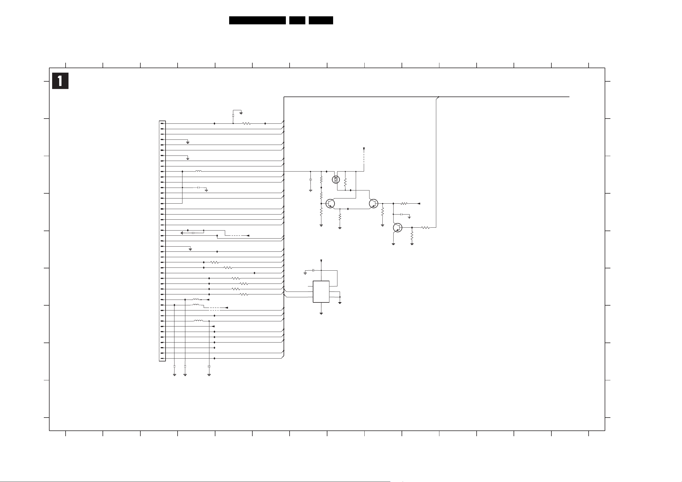
Servo Board: OPU Interface (Diagram 1) 14 28-29
Servo Board: Cheetah (Diagram 2
Servo Board: Laconic (Diagram 3) 16 28-29
Servo Board: Drivers (Diagram 4) 17 28-29
Servo Board: Centaurus (Diagram 5) 20 28-29
Servo Board: Power, Connectors (Diagram 6) 26 28-29
Servo Board: Tray Motor Connect.(Diagram 7) 27 28-29
8 Alignments 31
9 Circuit-, IC Descriptions and List
of Abbreviations 32
10 Electrical Parts List 47
) 15 28-29
©
Copyright 2003 Philips Consumer Electronics B.V. Eindhoven, The Netherlands.
All rights reserved. No part of this publication may be reproduced, stored in a
retrieval system or transmitted, in any form or by any means, electronic,
mechanical, photocopying, or otherwise without the prior permission of Philips.
Published by GH03 0395 Service PaCE Printed in the Netherlands Subject to modification EN 3122 785 13680
EN 2 VAD 80311.
Technical Specifications and Connection Facilities
1. Technical Specifications and Connection Facilities
1.1 VAD8031 functionality:
• Loading of 8 cm and 12 cm discs by a motorized tray
• Disc type recognition and in case of a DVD+RW disc laser
power calibration
• Servo control for disc rotation, sledge movements, tilt,
focus and actuator position
• EFM+ encoding / decoding for DVD, and EFM decoding for
CD
• Writes and read DVD+RW discs and reads DVD, CD and
CD-R/RW discs
• Linking control, header insertion and sector number
updating at record
• Interfacing to the MPEG back-end for control and for data
• The back-end has to provide MPEG data processing, data
buffering, construction of logical format for Lead-in, Data
area and Lead-out part of the DVD+RW disc
1.2 Connections
The following interfaces are provided for connecting the drive
to the MPEG back-end Application:
• Power Connector: 4-pin supply interface
• IDE Connector: 40-pin command and data transfer
interface
IDE Bus selection:
• Jumper Selection: 6-pin IDE Bus selector
Attention: Jumper has to be in position "Master"
1.3 Read and Write Speeds
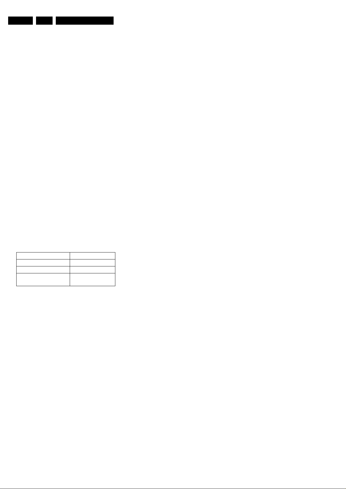
Type of Disc (Function) Disc Rotation Speed
Read Speed CD CAV 7x
Read Speed DVD CAV 4x
Write Speed DVD+RW
Write Speed DVD+R
ZCAV 2.4x
ZCAV 2.4x
Safety Instructions, Warnings and Notes
2. Safety Instructions, Warnings and Notes
EN 3VAD 8031 2.
2.1 Safety Instructions
2.1.1 General Safety
Safety regulations require that during a repair:
• Connect the unit to the mains via an isolation transformer.
• Replace safety components, indicated by the symbol ,
only by components identical to the original ones. Any
other component substitution (other than original type) may
increase risk of fire or electrical shock hazard.
Safety regulations require that after a repair, you must return
the unit in its original condition. Pay, in particular, attention to
the following points:
• Route the wires/cables correctly, and fix them with the
mounted cable clamps.
• Check the insulation of the mains lead for external
damage.
• Check the electrical DC resistance between the mains plug
and the secondary side:
1. Unplug the mains cord, and connect a wire between
the two pins of the mains plug.
2. Set the mains switch to the 'on' position (keep the
mains cord unplugged!).
3. Measure the resistance value between the mains plug
and the front panel, controls, and chassis bottom.
4. Repair or correct unit when the resistance
measurement is less than 1 MΩ.
5. Verify this, before you return the unit to the customer/
user (ref. UL-standard no. 1492).
6. Switch the unit ‘off’, and remove the wire between the
two pins of the mains plug.
2.1.2 Laser Safety
This unit employs a laser. Only qualified service personnel may
remove the cover, or attempt to service this device (due to
possible eye injury).
2.2 Warnings
2.2.1 General
• All ICs and many other semiconductors are susceptible to
electrostatic discharges (ESD, symbol ). Careless
handling during repair can reduce life drastically. Make
sure that, during repair, you are at the same potential as
the mass of the set by a wristband with resistance. Keep
components and tools at this same potential. Available
ESD protection equipment:
– Complete kit ESD3 (small tablemat, wristband,
connection box, extension cable and earth cable) 4822
310 10671.
– Wristband tester 4822 344 13999.
• Be careful during measurements in the live voltage section.
The primary side of the power supply (pos. 1005), including
the heatsink, carries live mains voltage when you connect
the player to the mains (even when the player is 'off'!). It is
possible to touch copper tracks and/or components in this
unshielded primary area, when you service the player.
Service personnel must take precautions to prevent
touching this area or components in this area. A 'lightning
stroke' and a stripe-marked printing on the printed wiring
board, indicate the primary side of the power supply.
• Never replace modules, or components, while the unit is
‘on’.
2.2.2 Laser
• The use of optical instruments with this product, will
increase eye hazard.
• Only qualified service personnel may remove the cover or
attempt to service this device, due to possible eye injury.
• Repair handling should take place as much as possible
with a disc loaded inside the player.
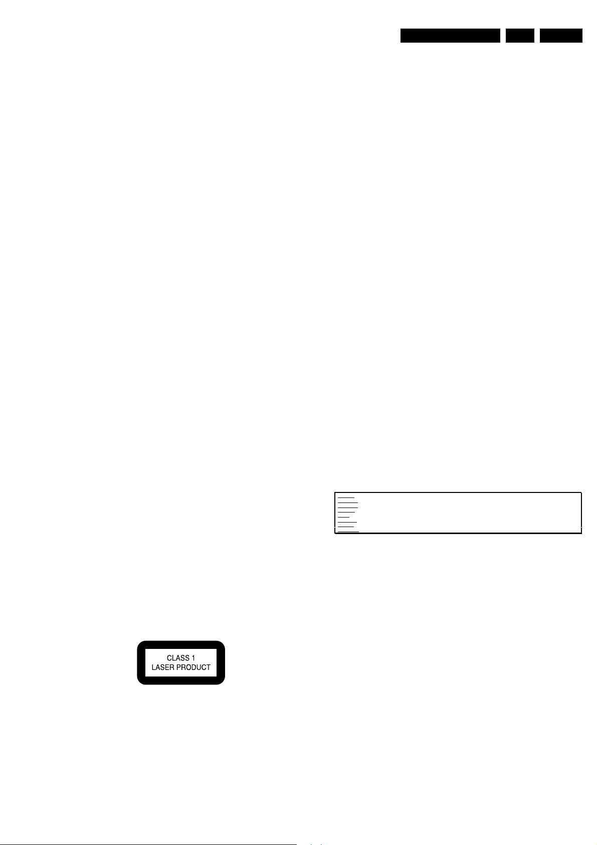
• Text below is placed inside the unit, on the laser cover
shield:
Laser Device Unit
Type : Semiconductor laser
GaAlAs
Wavelength : 650 nm (DVD)
: 780 nm (VCD/CD)
Output Power : 20 mW (DVD+RW
writing)
: 0.8 mW (DVD
reading)
: 0.3 mW (VCD/CD
reading)
Beam divergence : 60 degree
Figure 2-1 Class 1 Laser Product
Note: Use of controls or adjustments or performance of
procedure other than those specified herein, may result in
hazardous radiation exposure. Avoid direct exposure to beam.
CAUTION VISIBLE AND INVISIBLE LASER RADIATION WHEN OPEN AVOID EXPOSURE TO BEAM
ADVARSEL SYNLIG OG USYNLIG LASERSTRÅLING VED ÅBNING UNDGÅ UDSÆTTELSE FOR STRÅLING
ADVARSEL SYNLIG OG USYNLIG LASERSTRÅLING NÅR DEKSEL ÅPNES UNNGÅ EKSPONERING FOR STRÅLEN
VARNING SYNLIG OCH OSYNLIG LASERSTRÅLNING NÄR DENNA DEL ÄR ÖPPNAD BETRAKTA EJ STRÅLEN
VARO! AVATTAESSA OLET ALTTIINA NÄKYVÄLLE JA NÄKYMÄTTÖMÄLLE LASER SÄTEILYLLE. ÄLÄ KATSO SÄTEESEEN
VORSICHT SICHTBARE UND UNSICHTBARE LASERSTRAHLUNG WENN ABDECKUNG GEÖFFNET NICHT DEM STRAHL AUSSETSEN
DANGER VISIBLE AND INVISIBLE LASER RADIATION WHEN OPEN AVOID DIRECT EXPOSURE TO BEAM
ATTENTION RAYONNEMENT LASER VISIBLE ET INVISIBLE EN CAS D'OUVERTURE EXPOSITION DANGEREUSE AU FAISCEAU
!
Figure 2-2 Warning text

EN 4 VAD 80313.
3. Directions For Use
Not applicable
Directions For Use
4. Mechanical Instructions
Mechanical Instructions
EN 5VAD 8031 4.
Note that exploded views can be found in chapter 10
4.1 General
Follow the dismantling instructions in described order.
Do not place the unit with its PWB on a hard surface (e.g.
table), as it could damage the components on it.
Always place something soft (a towel or foam cushion) under it.
Never touch the lens of the OPU.
Take sufficient ESD measures during handling.
4.2 Dismantling
You can divide the Basic Engine into the following parts:
1. Loader (frame and tray, clamp)
2. PWB (or 'mono board')
3. DVD-Module (OPU, turntable motor, and sledge-motor
assy)
4. Encasing
4.3 Cab inet and Clamper Bridge
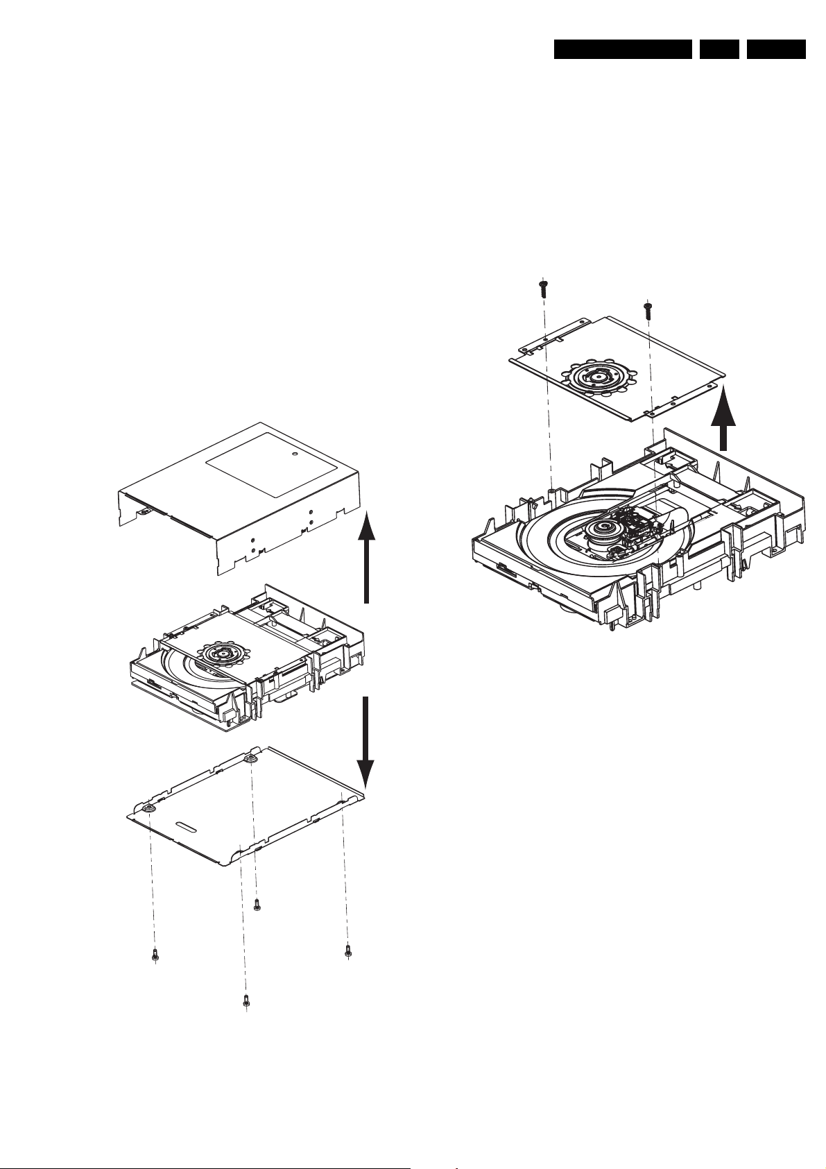
– Remove the encasing by releasing the four screws [1], see
figure 4-1
– Make sure that you do not lose the 5 heat paths (gray
rubber pieces that conduct the heat from the ICs to the
case)!
– Remove the clamper bridge assy, by releasing the two
screws [1], see figure 4-2
1
1
2
1
2
Figure 4-2 Remove Clamper Bridge
2
1
1
1
Figure 4-1 Basic Engine dismantling (part1)
EN 6 VAD 80314.
4.4 Tray
– Remove encasing as as described in 4.3
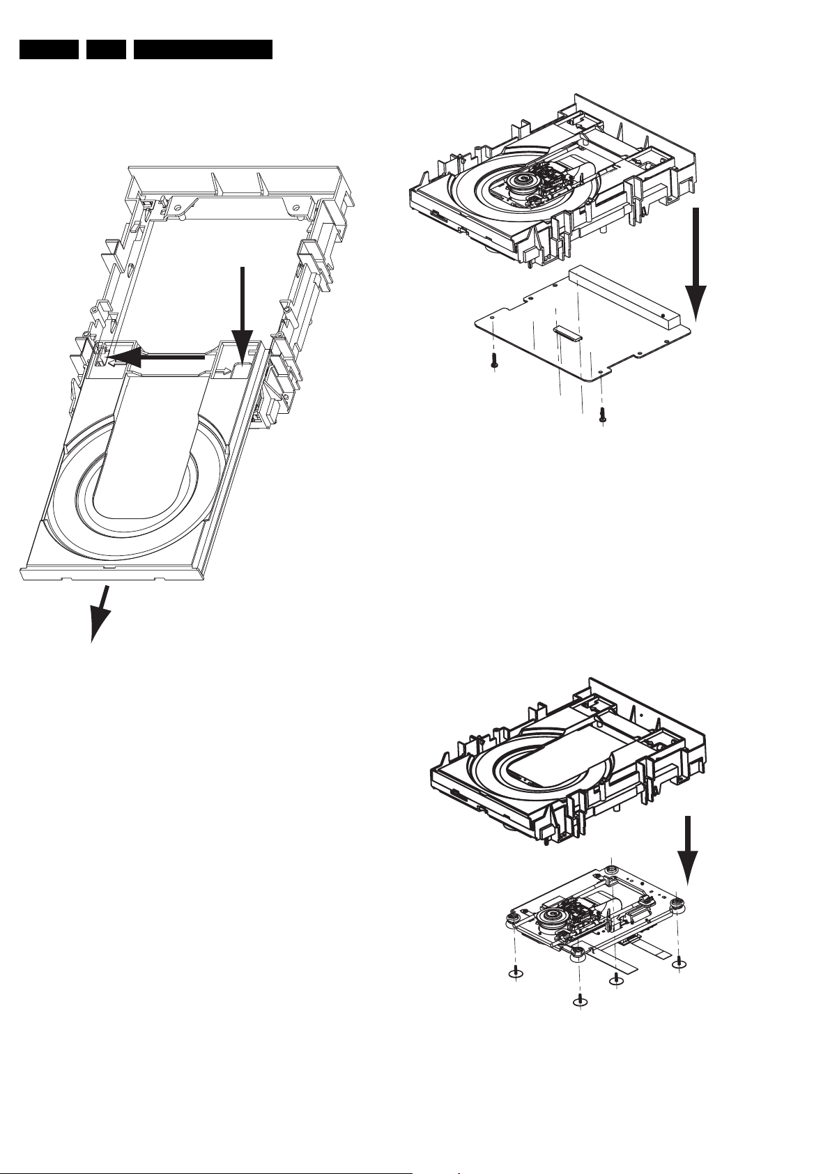
– Disengage the two holders that fix the tray [1], see figure 4-
3, and pull out the tray [2]
1
1
Mechanical Instructions
2
1
1
2
Figure 4-3 Remove Tray
4.5 Printed Board
Note: After Exchanging the PWB (or the DVD-M) the complete
drive has to be adjusted! Refer to chapter 8 for adjustment
instructions!
– Remove encasing and clamper bridge as described in 4.3
– Disconnect the four flex foils from the PWB connectors
– Remove the 2 screws that hold the PWB, see figure 4-4
– At assembly make sure that the 5 heat paths (gray rubber
pieces) are placed on the ICs!
Figure 4-4 Remove PWB
4.6 DVD-M
Caution: Never try to align or repair the DVD-Module itself!
Only the factory can do this properly. Service engineers are
only allowed to exchange the sledge motor assy.
After Exchanging the DVD-M (or the PWB) the complete drive
has to be adjusted! Refer to chapter 8 for adjustment
instructions!
– Remove encasing, clamper bridge and PWB as described
in 4-3 and 4-5
– Remove the four screws [1], see figure 4-5.
– Now you can remove the DVDM
2
1
1
Figure 4-5 Remove DVDM
1
1
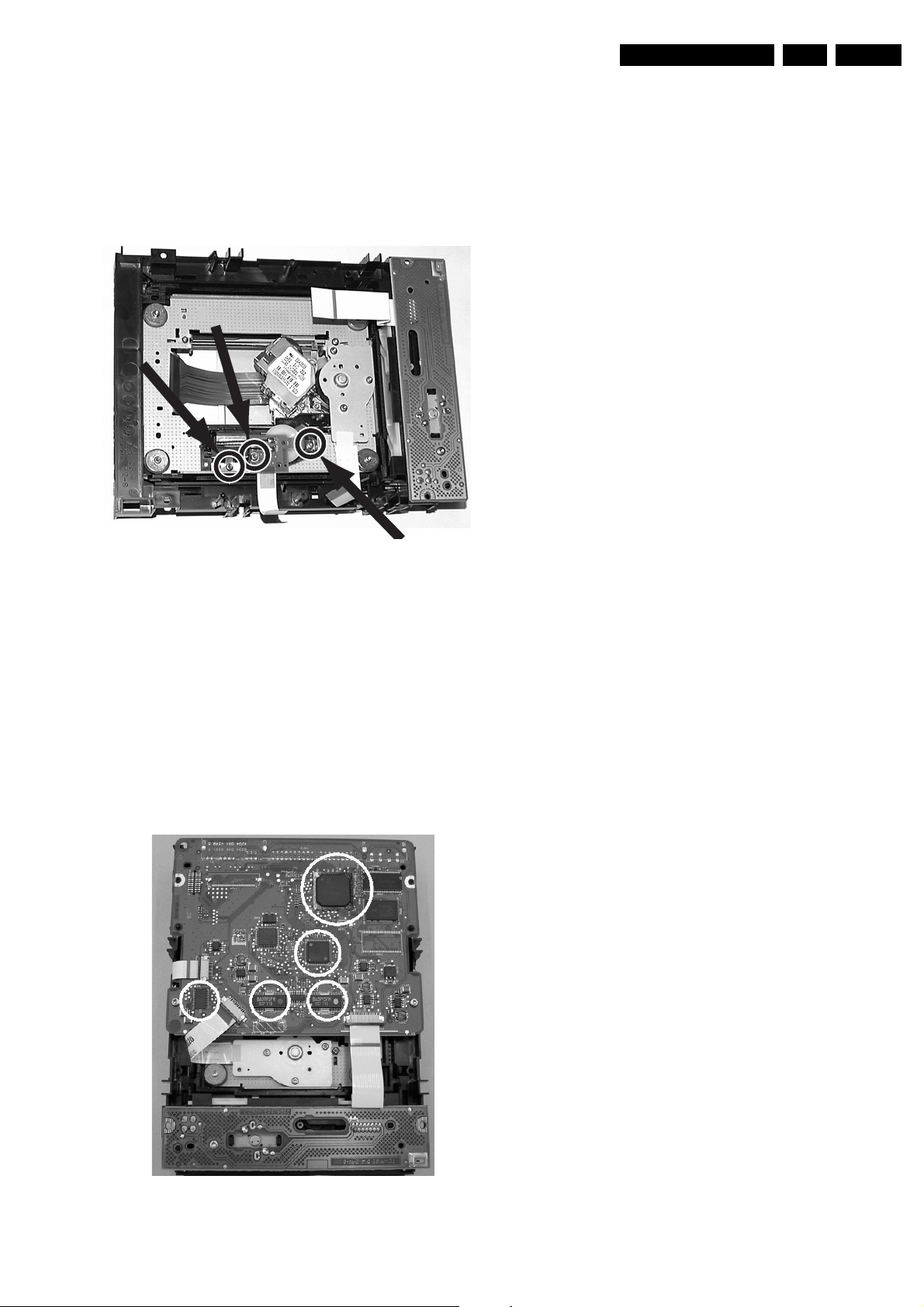
4.7 Sledge Motor Assembly
Caution: Never try to align or repair the DVD-Module itself!
Only the factory can do this properly. Service engineers are
only allowed to exchange the sledge motor assy.
– Place the DVD-Module, with the laser facing downwards
on a soft surface.
– Remove the three screws that hold the sledge-motor assy
and lift the assy upwards. You can replace it now.
Mechanical Instructions
EN 7VAD 8031 4.
Figure 4-6 Remove Sledge Motor Assy
4.8 Re-assembly
To re-assemble the module, do all processes in reverse order.
Take care of the following:
• Sledge-motor assy: Mesh the teeth of the sledge motor
and sledge rack properly, during mounting of the sledge
motor assy.
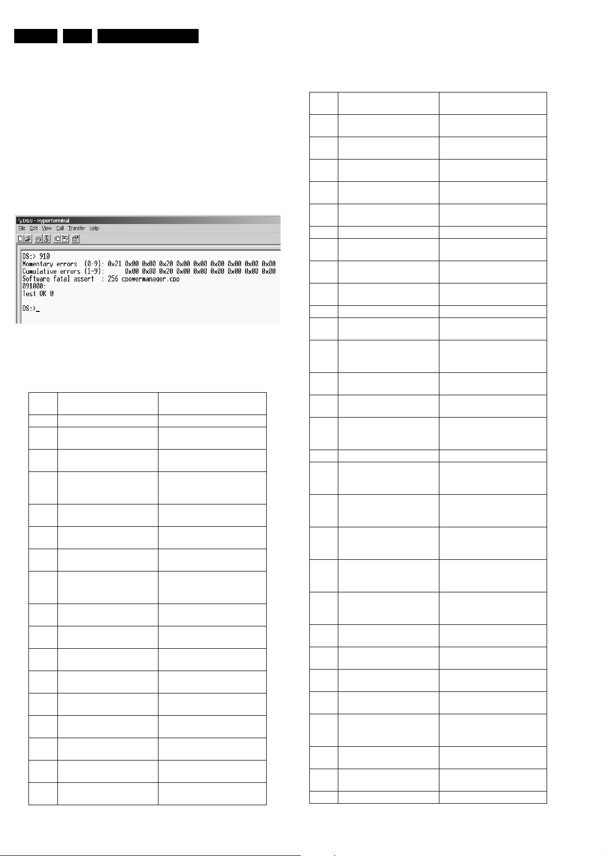
• Heat Paths: Put the 5 heat paths (gray rubber pieces) back
to their position on the ICs, see figure 4-7.
• Complete module: Place all wires/cables in their original
positions
• Emergency opening slot: Be sure that the slot for the
emergency tray opener is covered by adhesive tape!
• Jumper selection: Jumper has to be in position "Master"!
Figure 4-7 Heat Paths
EN 8 VAD 80315.
5. Diagnostic Software
Diagnostic Software
5.1 General
Please refer to the service manual of the recorder for a
description of the complete Diagnostics Software. In this
manual only drive specific error codes are explained.
5.2 Error Codes
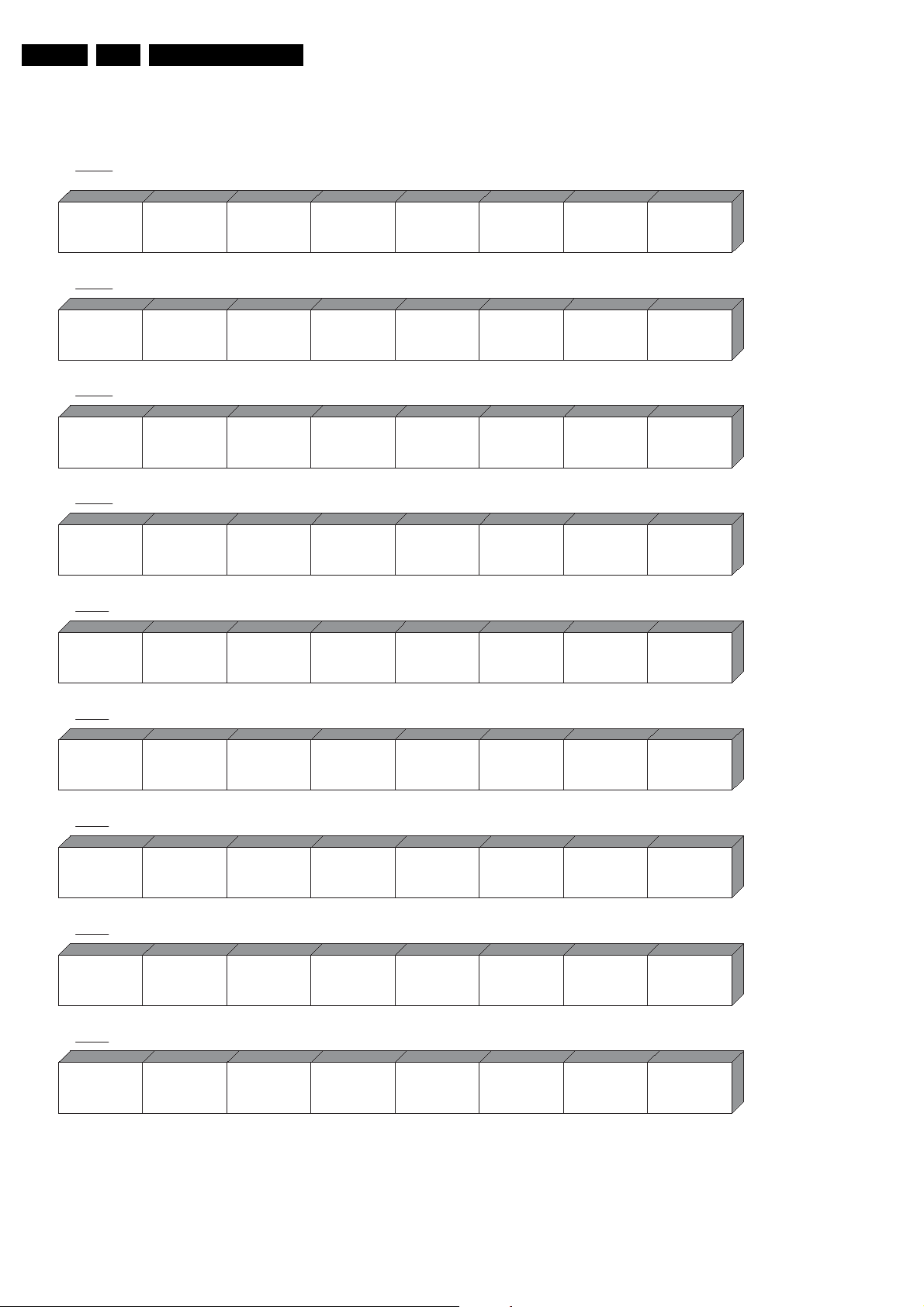
With DSW command 910 (Digital Board Chrysalis) the set
software can retrieve an overview of all occurred engine errors.
5.2.1 Momentary Errors
Byte 0: latest error:
Overview of the BE error codes.
error
error meaning
code
0x00 no_error No error has occurred
0x01 illegal_command_error Command not allowed in this
state or unknown command
0x02 illegal_parameter_error Parameter(s) not valid for
0x03 command_timeout_error The maximum execution
0x04 sledge_home_error The sledge could not be
0x05 sledge_calibration_error An error occurred during cal-
0x06 sledge_unstable_error The sledge detected unsta-
0x07 speed_timeout_error Spindle motor could not
0x08 speed_window_error Measured spinning speed is
0x09 focus_timeout_error Focus could not be achieved
0x0A focus_retries_error The amount of focus retries
0x0B focus_agc_error The focus agc results are out
0x0C radial_timeout_error Servo didn’t get on track
0x0D radial_retries_error Servo didn’t get on track after
0x0E radial_agc_error The radial agc results are out
0x0F radial_init_error Unreliable signal scaling af-
0x10 hf_pll_error HF-decoder pll could not lock
this command
time for the command has
exceeded
moved home
ibration of the sledge
ble control
reach its target speed within
timeout
not within expected window
within the timeout
expired
of range
within the timeout
several retries
of range
ter the radial initialisation
to HF signal
0x11 wobble_pll_error Wobble pll could not lock to
wobble signal
0x12 subcode_timeout_error Subcode information could
not be read
0x13 subcode_notfound_error Requested subcode item
0x14 header_timeout_error Header information could not
0x15 adip_timeout_error Adip information could not be
0x16 adip_window_error Adip address was not within
0x17 adip_sync_error No adip sync was detected
0x18 atip_timeout_error Atip information could not be
0x19 atip_notfound_error Requested atip item could
0x1A atip_window_error Atip address was not within
0x1B atip_sync_error No atip sync was detected
0x1C tray_error Tray could not be closed or
0x1D seek_error T he requested seek couldn’t
0x1E no_hf_present_error Attempt to read from a blank
0x1F record_error An error occurred during the
0x20 illegal_stopaddress_error The requested stopaddress
0x21 no_disc_error No disc is detected
0x22 not_initialised_error The system is not initialised
0x23 illegal_medium_error BE detected an unsupported
0x24 cd_frequency_error Measured HF frequency is
0x25 dvd_frequency_error Measured HF frequency is
0x26 re-
served(non_existing_bca_
error)
0x27 reserved(bca_read_error) An error occurred during
0x28 selftest_error An error occurred during the
0x29 i2c_error The I2C interface does not
0x2A laser_pll_error Laser control pll did not lock
0x2B laser_forward_sense_errorForward sense value didn’t
0x2C jitter_optimisation_error An error occurred during op-
0x2D tilt_calibration_error An error occurred during cal-
0x2E reserved
could not be found
be read
read
expected window
read
not be found
expected window
opened within the timeout
be performed within the timeout
area
recording
with modify-stop-address is
not valid
(e.g. seek on unknown disctype)
medium during disc recognition
not within CD frequency
range
not within DVD frequency
range
Attempt to read non-existing
bca information
reading of bca information
self-test of the BE
operate
or lost lock on write clock
change with changing laser
power
timisation of the jitter
ibration of the tilt frame

Diagnostic Software
EN 9VAD 8031 5.
0x2F frontend_offset_calib_errorThe offset in the frontend
0x30 reserved
0x31 wsg_calculation_error An error occurred in the cal-
0x32 buffer_overrun_error The buffer input stream over-
0x33 return_value_invalid_error The requested information is
0x34 illegal_recording_speed_e
rror
0x35 opc_media_parameter_errorThe media parameters (info
0x36 opc_record_power_error The final optimum power was
0x37 opc_start_power_low_errorOPC start power too low (op-
0x38 opc_start_power_high_errorOPC start power too high
0x39 opc_power_calculation_er
ror
0x3A opc_test_zone_full_error OPC can’t be performed be-
0x3B opc_bad_jitter_measurem
ent_error
0x3C opc_read_samples_error An error occurred during
0x3D ropc_alpha_overflow_error The determined value for the
0x3E ropc_alpha_ref_current_er
ror
0x3F ropc_alpha_gain_error The alpha measurement al-
0x40 beta_over_under_flow_errorDuring the walking OPC a
0x41 not_enough_calib_points_
error
0x42 not_enough_power_error The calculated power during
0x43 illegal_reading_speed_errorThe selected speed is not al-
0x44 servo_fatal_error The actuator dissipation be-
couldn’t be calibrated
culation of the write strategy
ran the buffer output stream
not available for this inquiry
The selected speed is not al-
lowed for a recording on this
medium
in ATIP/ADIP) are invalid or
not read
not reached
timum power is higher)
(optimum power is lower)
Error during OPC power cal-
culation (samples are wrong)
cause test zone is full
The jitter measurement dur-
ing OPC samples readback
failed
OPC readback sampling
optimum power is too high
The alpha measurement ref-
erence current is wrong (IAN)
pha gain is wrong
beta over-/under-flow was
detected
Not enough valid calibration
points available for re-calibration
re-calibration exceeds max
power
lowed for the requested command
came too high during a servo
recovery
This error is overwritten by the next player / inquiry command.
EN 10 VAD 80315.
Diagnostic Software
Byte 1 - 9: cumulative errors of previous error occurences.
Format of the BE error bytes
Every individual error has its own bit in the 9-byte structure as
described in the drawing below:
byte 1
b7 b6 b5 b4 b3 b2 b1 b0
reserved
FOCUS
AGC
ERROR
FOCUS
RETRIES
ERROR
FOCUS
TIMEOUT
ERROR
RADIAL
AGC
ERROR
RADIAL
RETRIES
ERROR
RADIAL
TIMEOUT
ERROR
byte 2
TRAY
ERROR
reserved
JITTER
OPTIMIZATION
ERROR
SLEDGE
HOME
ERROR
SLEDGE
UNSTABLE
ERROR
SLEDGE
CALIBRATION
ERROR
TILT SENSOR
OFFSET
CALIBRATION
ERROR
byte 3
RECORD
ERROR
SEEK
ERROR
NO DISC
ERROR
NOT
INITIALISED
ERROR
ILLEGAL
STOPADDRESS
ERROR
ILLEGAL
PARAMETER
ERROR
ILLEGAL
COMMAND
ERROR
byte 4
SERVO
FATAL
ERROR
reserved reserved
HF PLL
ERROR
NO HF
PRESENT
ERROR
HEADER
TIMEOUT
ERROR
SUBCODE
NOTFOUND
ERROR
RADIAL
INIT
ERROR
TILT
CALIBRATION
ERROR
COMMAND
TIMEOUT
ERROR
SUBCODE
TIMEOUT
ERROR
byte5
WOBBLE PLL
ERROR
byte6
WSG
CALCULATION
ERROR
byte7
LASER
FORWARD
SENSE
ERROR
byte8
OPC
READ
SAMPLES
ERROR
byte9
ADIP
SYNC
ERROR
DVD
FREQUENCY
ERROR
NVRAM
CHECKSUM
UPDATE
ERROR
OPC
BAD JITTER
MEASUREMENT
ERROR
ADIP
WINDOW
ERROR
CD
FREQUENCY
ERROR
FRONTEND
OFFSET
CALIBRATION
ERROR
OPC
TEST ZONE
FULL
ERROR
ADIP
TIMEOUT
ERROR
ILLEGAL
RECORDING
SPEED
ERROR
LASER PLL
ERROR
OPC
POWER
CALCULATION
ERROR
ATIP
NOTFOUND
ERROR
SPEED
WINDOW
ERROR
ILLEGAL
READING
SPEED
ERROR
OPC
START
POWER HIGH
ERROR
ATIP
SYNC
ERROR
SPEED
TIMEOUT
ERROR
ILLEGAL
MEDIUM
ERROR
OPC
START
POWER LOW
ERROR
ATIP
WINDOW
ERROR
NON
EXISTING
BCA
ERROR
SELFTEST
ERROR
OPC
RECORD
POWER
ERROR
ATIP
TIMEOUT
ERROR
BCA
READ
ERROR
I2C
ERROR
OPC
MEDIA
PARAMETER
ERROR
RETURN
VALUE
INVALID
ERROR
BUFFER
OVERRUN
ERROR
BETA
OVER/UNDER
FLOW
ERROR
NOT ENOUGH
CALIB POINTS
ERROR
These errors are kept in memory until a power down of the
drive (e.g. when recorder goes to standby) or reset of the drive.
NOT ENOUGH
POWER
ERROR
ROPC
ALPHA
GAIN
ERROR
ROPC
ALPHA
REF CURRENT
ERROR
ROPC
ALPHA
OVERFLOW
ERROR

5.2.2 Cumulative errors
These errors are stored in EEPROM and are thus non-volatile
showing the complete error history of the drive.
Byte 1 - 9: cumulative errors of previous player / inquiry error
occurences. These bytes are the same as the nine bytes (1-9)
of the Momentary errors
5.2.3 Software fatal assert
Gives row number and file name in the source code of the
firmware of the data path of the AV
Diagnostic Software
EN 11VAD 8031 5.

EN 12 VAD 80315.
Diagnostic Software
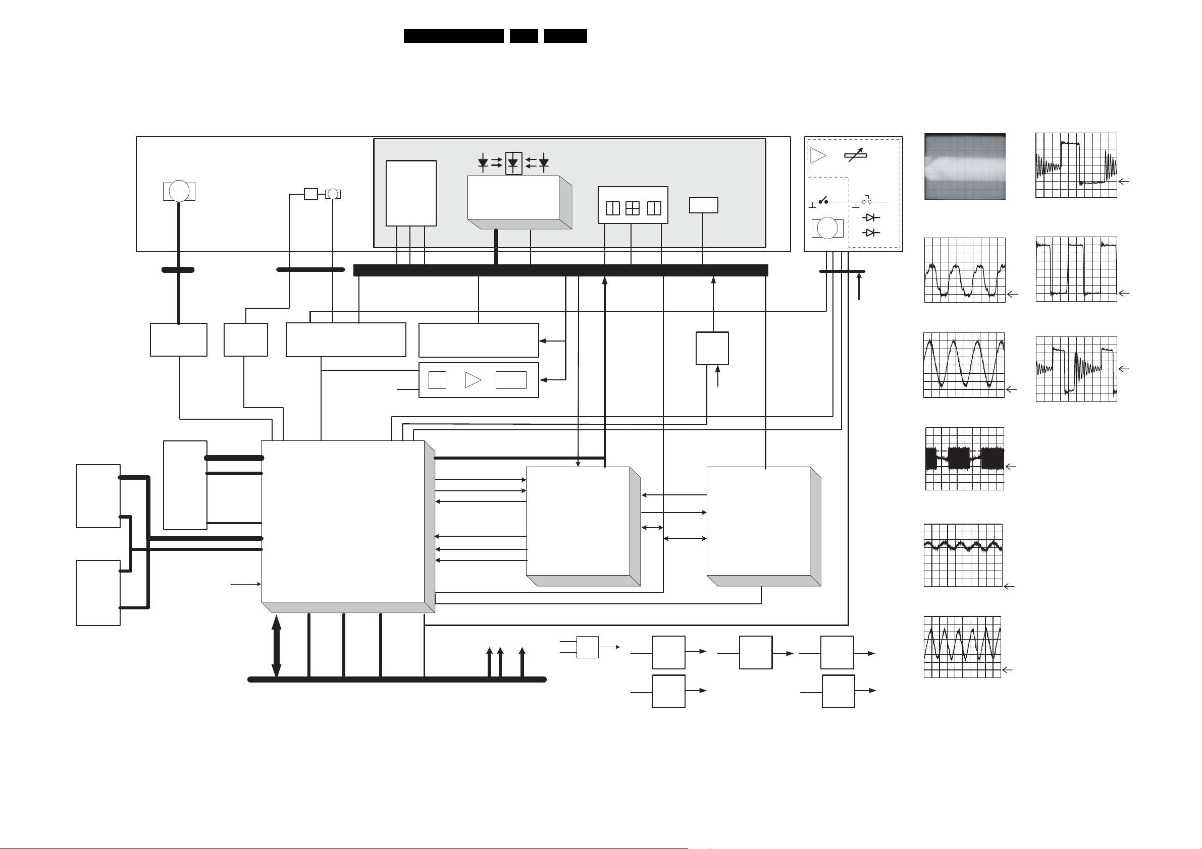
6. Block Diagram.
Block Diagram
Disc Motor
M
11P
1401
7402
Disc Motor Driver
option
SRAM
7503
TZA1015
7504
SDRAM
16MB
U,V,W coil
U+,UV+,VW+,WHall+ ,Hall-
MOTO1
MOTOR-ON
VMOTO10
T1
7400
XDD0..15
XDA0..11
DATA_MASK
DA0..15
AD0..19
PCS-p re_amp
SIN H
COSPH
REFSIN
REFCOS
7500
XWR
XRAS
SDCK
XCASL
XCASH
1400
LOADER
+SI N , - SIN
+COS, -COS
7409
ROHM
Block Diagram.
PCS
Sled g e
M
9P
SL-
SL+
Servo D ri v e r
BA5995FM
SL
FO+
FORA
TRAY-INOUT
TRAY-ONOFF
DRIVER-ON
CENTAURUS
FOC+
FOC-
Actuator
RADIAL
FOCUS
TILT
1V65
7408
7405
DC
level
laser 650nm
RAD
Servo D r iv er
BA5995FM
SID A , SILD, SICL
RFREF
RFN3 ,RFP3
A1,2
CALF
XDN
FTC
D1..4
PPNO
F S diode
E la ntec 6295
SCLK
SDI O
SEN
offset
gain
TRAYSW
EJECTKEY
DEBUG1,2,4,5
laser 780nm
EFM
R/ W
SERVO-M EA S
SERVO-COM M
FOC-
FOC+
13VAD 8031 6.
650nm PD
RAD
OPU66
PAEDIC
TZA 1045
CD-MO DE
VIA..H RF P ,R F N IIC
HIGH-GAIN
VIA..H
RFP
RFN
E FMDATAP
EFM _ D A TA
EFM CLKN
EFM CLKP
EFM _ RWN
7201
highpower
IIC
LASP
ALFA
EEpr o m
7104
PAEDIC
power
7300
4V6
1002 Tr a y Motor PWB Assy
option
for Data
Drive
Headphones
Tray Switch
Eject key
R F N3 / R F P3, IC 7201 P in 38/39
A:AC, 50mV/Div
50ns/Div
M
15P
5V
3V3
LED
1702
Tr a y Motor
OPU Flex 45p
1100
Iodel
IOthr
IAPC
WSB
SCLK
SDIO
SEN
RW-Del
Vdel
5V
VREF
Vthr
HIGH-GAIN
CD- M ODE
LACONICCHEETA H
TR+
TR-
IC7300 Pin 4
A: DC , 1 V /Div, 20ns/Div
IC7300 Pin 5
A: DC , 500mV/Div, 20ns/Div
1401 Pin 9/10/11
A: DC , 5 V /Div, 500us/Div
1400-2,3,4,6,7, 8
IC 7604 P in 4
A: DC , 1 V/Div, 1us/Div
IC 7606 P in 1
A: DC , 2 V/Div, 1us/Div
IC 7605 P in 7
A: DC , 2 V/Div, 1us/Div
FLASH
PROM
1600
PORN
HD0..15
IDE
HDASPN
CS0
CS1
HA0
HA1
HA2
HPDIAGN
HIRQ
HDACKN
IOR DY
HDRN
HRWN
HDRQ
RX1_MASTER
TX1
TX2
DEBUG11
AUDIOR
AUDIOL
IEC958
5V
From/To DVD Recorder application
GND
12V
IR Q N,OSTR,EFM_RW N
1V8
3V3
RESET
PORN
7502
7603
5V
12V
3v3 1V8
5V25
5V
7606
7604
TOSTOCEN
A: DC , 500mV/Div, 2ms/Div
IC7504 Pin 38
7605
5V
-5V
1V65
TR 15001_002
100903
A: DC , 500mV /Div, 5ns/Div
Electrical Diagrams and Print-Layouts
7. Electrical Diagrams and Print-Layouts
Servo Board: OPU Interface
14VAD 8031 7.
1 2 3 4 5 6 7 8 9 10 11 12 13 14
1100 A3
2100 C4
2101 H4
A
2102 E4
2103 A5
2104 H3
2105 H4
2106 D9
TO CHEETAH_QD/DRIVERS/CENTAURUS-DRAM-FLASHROM/DEBUG-AND-FLASH
{SERVO-MEAS,VREF,Vdel,Vthr,ENA,RW-Del,HIGH-GAIN,CD-MODE,VIG,VIE,VIA,VID,RFP,RFN,VIB,VIC,VIH,VIF,SERVO-COMM,FOC-,FOC+,RAD,IOthr,EFM-DATAP,EFM-DATAN,EFM-CLKP,EFM-CLKN,EFM_RWN,SCLK,SDIO,SEN,BUSY,IoDel,WSB,SCL,SDA,HIGHPOWER}
A
2107 C7
B
C
D
E
F
G
H
2108 F7
2110 B7
3100 E5
3101 E4
3103 F5
3104 B5
3105 F5
3106 F5
3107 F5
3110 D10
3111 E10
3112 D9
3113 D10
3114 D8
3115 C8
3116 C7
3117 D7
3118 D7
3119 B7
3120 A7
4100 D7
4105 G4
4106 C8
4107 C8
4108 C8
4109 D5
4110 E5
4111 F4
4112 G4
5101 C4
5102 F4
5103 F4
5104 G4
7101 D9
7102 D9
7103 D8
7104 C8
7105 F7
7107 B8
I100 B4
I101 B6
I102 F6
I103 G4
I104 G4
I106 G4
I107 H4
I108 G5
I110 E4
I111 E4
I115 D4
I116 F4
I117 F4
I118 F4
I119 F4
I120 C4
I121 C8
1100
AF3
45
44
43
B
C
D
E
F
G
42
41
40
39
38
37
I120
36
35
34
33
32
31
30
29
28
27
26
25
24
23
22
21
20
19
18
17
16
15
14
13
12
11
10
9
8
7
6
5
4
3
2
1
I115
100n
I128
I129
5102
5103
2102
5101
2100
100n
5104
I100
I130
I131
I110
3101
I111
82R
I116
I117
I118
I119
D3V3
4112
4105
I104
I103
I106
L100
I107
I108
+12V
10u
3100
100p
2103
3104
100R
4110
82R
3103
1K1K3105
3106
1K
3107
1K
+5V25
+5V25
I102
I101
HIGH-GAIN
EFM-DATAP
EFM-DATAN
SERVO-MEAS
SERVO-COMM
RW-Del
CD-MODE
VREF
SDIO
SCLK
EFM_RWN
EFM-CLKN
EFM-CLKP
WSB
IOthr
IoDel
FOC-
FOC+
RAD
VIG
VIE
VID
VIA
RFN
RFP
VIC
VIB
VIH
VIF
SCL
SDA
Vdel
Vthr
SEN
SDA
SCL
2107
2108
100n
LM75ADP
3
1
2
I121
1K5
22u
3116
7104
BSH205
7103
BC847B
7
6
5
3114
3115
820R
I122
3117
220R
I124
1K
3118
D3V3
8
7105
+VS
A0
OS
SDA
A1
SCL
A2
GND
4
+5V25
4108
3K3
I123
3112
1K
7102
BC847B
I125
2106
100n
7101
BC847B
I126
3113
3V3
1K0
I127
10K
3111
HIGHPOWER
3110
10K
H
2101
2104
100n
2105
100n
220p
I122 C7
I123 C8
I124 D7
I125 D9
I126 D8
I
I
I127 D10
I128 F4
I129 F3
I130 E5
I131 E5
TR 15002_001
100903
I132 A8
I133 B7
L100 H4
1 2 3 4 5 6 7 8 9 10 11 12 13 14
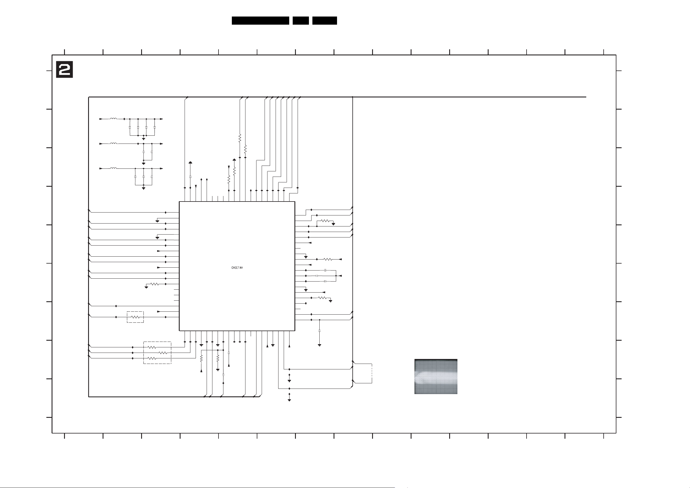
Servo Board: Cheetah
Electrical Diagrams and Print-Layouts
15VAD 8031 7.
1 2 3 4 5 6 7 8 9 10 11 12 13 14
A
5202
5204
5201
I201
2209
100n
5VA
B
-5V
C
-5V
2206
D
VIH
VIC
VIB
RFN
E
RFP
VID
VIA
VIE
VIG
F
TIMOUT
EFM-CLKN
G
EFM-CLKP
EFM-DATAN
H
EFM-DATAP
I253
I254
CLOSE TO IC7500
3209
1K8
I261
I262
I263
I
{TIMOUT,RFP,RFN,VIA,VIB,VIC,VID,VIE,VIF,VIG,VIH,EFM-CLKP,EFM-CLKN,EFM-DATAP,EFM-DATAN,TS1,TS2,LASP,PPNO,RFP3,RFN3,RFREF,CALF,A1,A2,XDN,D1_TILTN,D2_TLN,D3_REN,D4_FEN,S1_MIRN,S2,MON1,MON2,SIDA,SICL,SILD,SDA,SCL,ALFA,FTC,VERSION0,VERSION1,RW-Del,R-W,GEN-INP0,GEN-INP1,EFMCLK-O,EFM_DATA_P_del,EFM_DATA_N_del,EFM-DATAP,EFM-DATAN,RWN,PORN,EFM_RWN}
A1
VIF
LASP
ALFA
A2
CALF
XDN
D2_TLN
D1_TILTN
D3_REN
TO OPU/EPLD-LADIC-CON/LACONIC_IC/CENTAURUS
+5Vd
2212
100n
100n
2211
100n
2210
3201
3205
I225
72
NC8
CFTC
29
2217
10n
I243
10K
3203
1%
47K
I209
71
TEST
TZA1039HL
30
I246
I245
47n
100R
3200
100R
I242I244
I203
D163D262D3
VDD1-3
GND1-4
VSS1-2
CCALF
GND1-3
VSS1-1
SERTST
RFREF
RFP
RFN
39
-5Va
61
MON2
MON1
CMPP
RREF
CA2
CA1
PPN
NC7
NC6
VSS2
I202
I216
I217
60
D4
59
S1
58
S2
57
56
55
54
53
52
51
I234
50
I237
49
I239
48
47
46
45
L201
44
43
42
41
40
I219
I221
I222
I236
I238
I241
+5Vd
I228
-5Va
2214
3214
27K
2213
2215
10n
10n
3208
10K
2223
27n
100n
3206
47K
-5Vd
D4_FEN
S1_MIRN
S2
MON2
MON1
-5Va
1%
-5Va
PPNO
RFREF
69
70
ALFA
LASP
TS131TS2
SILD
32
SROUT
NC5
33
A167A2
34
65
64
XDN
CALF
VDD2
SICL35SIDA
GND2
37
36
38
I204
I207
I205
I208
I206
L200
68
66
+5Vd
RFN3 / RFP3, IC7201 Pin 38/39
TIMOUT
RFN3
4201
RW-Del
RFP3
SILD
SIDA
SICL
I257
I258
I259
I260
I256
100n
2219
2207
-5Vd
100n
2220
100n
-5Va
100n
2222
100n
I215
I218
I220
I224
I226
+5Vd
I227
I229
+5Vd
I231
I233
I235
3207
10K
-5Vd
I240
CLOSE TO IC7500
3210
3211
1K8
3212
1K8
1K8
7201
-5Va
100n
2221
I223
I214
-5Va
I212
I265
78
79
80
VIF
VREF
VIH
GND1-1
VIC
VIB
GND1-2
RFNIN
RFPIN
VDD1-1
VID
VIA
VDD1-2
VIE
VIG
R|W
NC1
NC2
NC3
TIMOUT
VSSD
EFMCN
I252
EFMCP21EFMDN
22
I251
I250
VSS1-3
EFMDP
23
1
2
3
4
5
6
7
8
9
10
11
12
13
14
15
16
17
18
19
20
3217
77
WRF
GNDD
74MI73
75
76
LD
RRF
VDDL
SCL26SDA
NC4
I248
27
3213
FTC
28
I247
18K
24
25
I249
33K
-5Va
+5Vd
2218
I264
SDA
SCL
FTC
A:AC, 50mV/Div
50ns/Div
2204 B5
2205 B5
2206 C2
2207 C3
2209 B2
2210 B2
2211 B3
2212 B3
2213 F7
2214 F7
2215 F7
2217 H5
2218 H5
A
2219 C3
2220 C3
2221 C4
2222 C3
2223 G7
3200 C5
3201 B5
3202 C4
3203 C5
3204 C4
3205 C5
3206 E7
B
3207 F3
3208 F7
3209 G2
3210 H3
3211 H3
3212 H3
3213 H4
3214 D7
3215 D3
3216 D3
3217 H4
4200 H9
C
4201 H8
5201 C2
5202 B2
5204 B2
7201 D3
I201 B2
I202 D6
I203 D6
I204 D6
I205 D6
I206 D6
D
I207 D6
I208 D5
I209 D5
I212 D4
I214 C4
I215 D3
I216 D7
I217 D7
I218 D3
I219 D7
I220 E3
I221 E7
E
I222 E7
I223 C4
I224 E3
I225 D5
I226 E3
I227 E3
I228 E7
I229 E3
I231 F3
I233 F3
I234 F7
I235 F3
F
I236 F7
I237 F7
I238 G7
I239 F7
I240 G3
I241 G7
I242 C5
I243 C5
I244 H5
I245 H5
I246 H5
G
I247 H5
I248 H4
I249 H4
I250 H4
I251 H4
I252 H4
I253 G2
I254 G2
I256 B2
I257 H6
I258 H6
I259 I6
H
I260 I6
I261 H2
I262 H2
I263 H2
I264 I5
I265 D4
L200 D5
L201 F7
I
TR 15003_001
1 2 3 4 5 6 7 8 9 10 11 12 13 14
100903
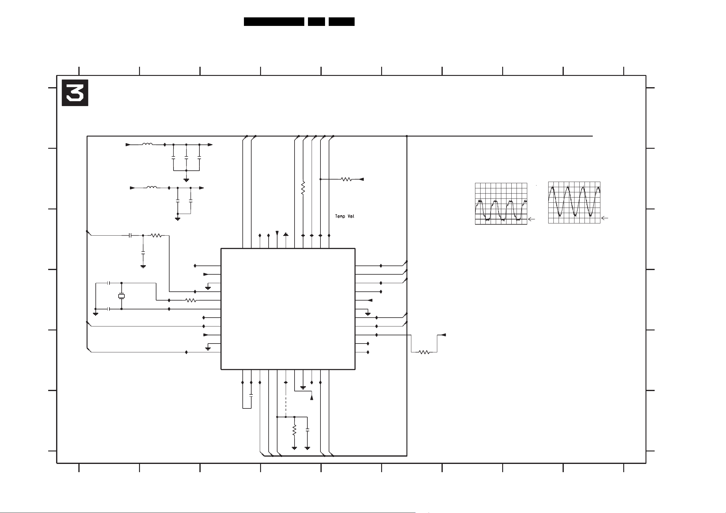
Servo Board: Laconic
A
B
OSC_IN
C
2303
D
ALFA
LASP
E
Electrical Diagrams and Print-Layouts
16VAD 8031 7.
1 2 3 4 5 6 7 8 9
TO OPU/EPLD/CENTAURUS
{WSB,RW-Del,R-W-Delayed,TIMOUT,OSC_IN,PORN,VERSION0,VERSION1,SCL,SDA,SCLK,SDIO,SEN,BUSY,ENA,HIGH-GAIN,CD-MODE,GEN-INP0,GEN-INP1,EFM-CLKP,EFM-CLKN,EFMDATA-3P,EFMDATA-3N,ALFA,LASP,Vdel,Vthr,VREF,IOthr,CD-MODE,HIGH-GAIN,IRQN,OSTR,RWN,SDA,SCL,IoDel}
5300
5301
15p
3303
150R
I303
I313
I308
I310
2301
2306
2302
100n
100n
I312
D3V3
A3V3 3V3A
2311
1n0
2312
15p
1302
16M93
2304
15p
CX-16F
2307
3315
33R
100n
2300
100n
3V3D
I320
3V3A
L308
L303
I311
100n
3V3D
1
2
3
4
5
6
7
8
9
10
11
AEZ
Vddd3
Vssd3
ClckOut
Osco
Osci
Test1d
Ameas
Vdda1
Vssa1
LasP
SCL
I316
SDA
44
SCL
VRefL
12
I317
L301
43
SDA
VRefH
13
L305
L307
42
Test2d
VDel
14
3V3D
41
Bank
VThr
15
39
40
Vssd2
Vddd2
7300
LACONIC
Vopuref16Vrefin
17
I314
RW-Del
38
RWn
Vdda2
18
PORN
3302
I304
37
Resetn
Vssa2
19
OSTR
1R
I305
36
OSTR
Test1a
20
L306
IRQN
I306
35
IRQn
IoDel
21
L310
WSB
L311
34
WSB
IoThr
22
3316
10K
SCLK
SDIO
SEN
Busy
Vddd1
Vssd1
HiLo
DvdCd
EnR1
EnR2
Test2a
3V3D
L309
L304
3V3D
I302
I315
I318
I300
I301
I319
SCLK
SDIO
SEN
HIGH-GAIN
CD-MODE
3V3D
3301
10K
33
32
31
30
29
28
27
26
25
24
23
IC7300 Pin 4
A: DC, 1 V/Div, 20ns/Div
IC7300 Pin 5
A: DC, 500mV/Div, 20ns/Div
A
B
C
D
E
1302 D1
2300 B2
2301 B2
2302 B2
2303 D1
2304 D1
2305 F3
2306 B2
2307 B2
2308 B5
2309 E6
2310 F4
2311 C1
2312 C2
3300 D2
3301 E6
3302 B4
3303 C2
3304 E5
3305 E5
3306 E6
3308 F4
3309 F4
3315 D2
3316 B5
4303 F4
5300 A2
5301 B2
7300 D4
I300 C5
I301 D5
I302 D5
I303 A2
I304 C4
I305 C4
I306 C4
I307 C1
I308 D2
I310 D2
I311 D3
I312 E2
I313 B2
I314 E4
I315 D5
I316 E3
I317 E3
I318 D5
I319 D5
I320 D2
L301 C3
L303 D3
L304 E5
L305 E3
L306 E4
L307 C4
L308 C3
L309 E5
L310 E4
L311 C5
F
22n
2305
Vdel
Vthr
4303
VREF
3309
1K8
3V3A
2310
100n
IoDel
IOthr
1 2 3 4 5 6 7 8 9
TR 15004_001
100903
F
 Loading...