

Philips UZZ9001 Datasheet

DISCRETE SEMICONDUCTORS
DATA SH EET
UZZ9001
Sensor Conditioning Electronic
Product specification
Supersedes data of 2000 May 19
2000 Nov 27

Philips Semiconductors Product specification
Sensor Conditioning Electronic UZZ9001
FEATURES
• One chip angle sensor output signal conditioning
• 180° angle range with KMZ41
• Accuracy better than 1° together with KMZ41
• Temperature range from −40 to +150 °C
• SPI protocol
• SO24 package.
GENERAL DESCRIPTION
The UZZ9001 is an integrated circuit that combines two
sinusoidal signals (sine and cosine) into one single linear
output signal. These signals might come from the
magnetoresistive sensor KMZ41. This results in a
measurement system for angles up to 180°. The
integrated circuit UZZ9001 can also be used for all other
applications in whichan angle has to be calculated from a
sine and cosine signal. A typical application would be any
kind of resolver application.
The two input signals are converted into the digital domain
with two separate AD converters. A CORDIC algorithm
performs the inverse tangent transformation. The output
stage implements the Motorola Serial Peripheral Interface
(SPI) protocol.
PINNING
SYMBOL PIN DESCRIPTION
+V
+V
V
V
O2
O1
DD2
SS
1 sensor 2 positive differential input
2 sensor 1 positive differential input
3 digital supply voltage
4 digital ground
GND 5 analog ground
RST 6 reset of the digital part; note 1
TEST1 7 for production test; note 1
TEST2 8 note 2
DATA_CLK 9 trim-mode data-clock; note 1
SMODE 10 serial mode programmer; note 1
TEST3 11 note 2
data 12 SPI data output
CLK 13 SPI data clock in
CS 14 SPI chip select
OFFS2 15 offset trimming input sensor 2
OFFS1 16 offset trimming input sensor 1
V
DDA
17 analog supply voltage
GND 18 analog ground
TEST4 19 for production test; note 1
TEST5 20 for production test; note 1
V
T
−V
−V
DD1
out
O2
O1
21 digital supply voltage
22 test output
23 sensor 2 negative differential input
24 sensor 1 negative differential input
Notes
1. Connected to ground.
2. Pin to be left unconnected.
QUICK REFERENCE DATA
SYMBOL PARAMETER CONDITIONS MIN. TYP. MAX. UNIT
V
DDA
V
DD1
V
DD2
I
CCtot
supply voltage note 1 4.5 5 5.5 V
supply voltage note 1 4.5 5 5.5 V
supply voltage note 1 4.5 5 5.5 V
total supply current no output load − 515mA
Res resolution − 13 − bit
A accuracy with ideal input signal ±0.35 −−deg
I
data-out
peak output current −−10 mA
Note
1. V
DDA
, V
DD1
and V
must be connected to the same supply voltage.
DD2
2000 Nov 27 2

Philips Semiconductors Product specification
Sensor Conditioning Electronic UZZ9001
LIMITING VALUES
In accordance with the Absolute Maximum Rating System (IEC 60134).
SYMBOL PARAMETER CONDITIONS MIN. MAX. UNIT
V
DDA
V
DD1
V
DD2
V
pin
T
stg
T
amb
THERMAL CHARACTERISTICS
SYMBOL PARAMETER VALUE UNIT
R
th j-a
supply voltage −0.3 +6 V
supply voltage −0.3 +6 V
supply voltage −0.3 +6 V
voltage at all pins −0.3 V
DD
V
storage temperature −55 +150 °C
operating temperature 125 to 150 °C; max 200 hours −40 +150 °C
thermal resistance from junction to ambient 80 K/W
ESD SENSITIVITY
SYMBOL PARAMETER CONDITIONS VALUE UNIT
ESD ESD sensitivity human body model 2 kV
machine model ±150 V
2000 Nov 27 3

Philips Semiconductors Product specification
Sensor Conditioning Electronic UZZ9001
ELECTRICAL CHARACTERISTICS
T
= −40 to +150 °C; VDD= 4.5 to 5.5 V; typical characteristics for T
amb
specified.
SYMBOL PARAMETER CONDITIONS MIN. TYP. MAX. UNIT
V
DDA
V
DD1
V
DD2
I
DD
(+V
)-(−VO) differential input voltage referred to V
O
f
ext
f
int
I
o
supply voltage 4.5 5 5.5 V
supply voltage 4.5 5 5.5 V
supply voltage 4.5 5 5.5 V
supply current without load − 515mA
DD
common mode range referred to V
lost magnet threshold referred to V
DD
DD
external clock frequency for trim interface 0.1 − 1 MHz
internal clock frequency 2.3 4 5.7 MHz
data output constant current −−1mA
peak current −−10 mA
V
reset
switching voltage between falling and
threshold
rising V
DD
hysteresis − 0.3 − V
A accuracy with ideal input signal ±0.35 −−degree
Res resolution − 13 − bit
t
on
t
r
V
ID
power up time −−20 ms
response time to 95% of final value − 0.7 1.2 ms
digital input voltage LO signal 0 − 0.3xV
HI signal 0.7 x V
V
OD
digital output voltage LO signal −−0.4 V
HI signal V
V
LM
sensor voltage lost magnet threshold 12 15 20 mV
=25°C and VDD= 5 V unless otherwise
amb
±6.6 −±28 mV/V
490 − 510 mV/V
−3−mV/V
2.8 − 4.5 V
V
DD
− V
DD
−0.8 −−V
DD
DD
V
FUNCTIONAL DESCRIPTION
The UZZ9001 is a mixed signal IC for angle measurement
systems. It combines two analog signals (sine and cosine)
into a linear output signal. The output stage implements
the Motorola Serial Peripheral Interface (SPI) protocol.
The UZZ9001 has been designed for use with the double
sensor KMZ41.
The analog measurement signals on the IC input are
converted to digital data with two ADC’s. The ADC’s are a
Sigma-Delta modulator employing a 4th order continuous
time architecture with an over-sampling ratio of 128 to
achieve high resolution. The converter output is a digital
bitstream with an over-sampling frequency of typically
500 kHz.
2000 Nov 27 4
The bitstream is fed into a decimationfilter which performs
both low pass filtering and down-sampling. TheIC has two
input channels each of which has its own ADC and
decimation filter. The two decimation filter outputs are
15-bit digital words at a lower frequency of typically
3.9 kHz which is the typical sampling frequency of the
sensor system. The digital representations of the two
signals are then used to calculate the current angle. This
calculation is carried out using the so-called CORDIC
algorithm. The angle is represented with a 13-bit
resolution. An SPI compatible interface converts the
output word to the serial peripheral interface protocol.
Philips Semiconductors Product specification
Sensor Conditioning Electronic UZZ9001
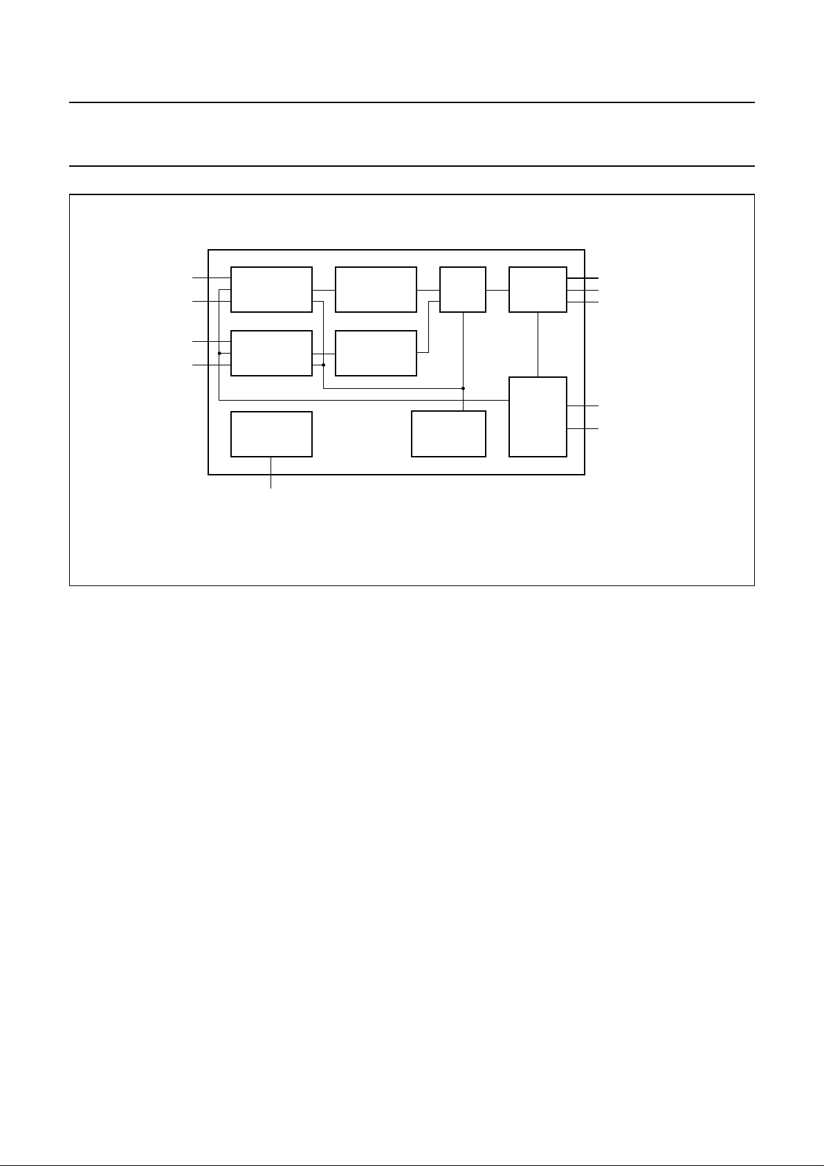
handbook, full pagewidth
+V
−V
+V
−V
O1
O1
O2
O2
ADC1
ADC2
DECIMATION
FILTER
DECIMATION
FILTER
ALU SPI CLK
data
CS
RESET
reset
UZZ9001
Fig.1 Block diagram.
The following list gives a short description of the relevant
block functions:
1. The ADC block contains two Sigma Delta AD
converters, sensor offset correction circuitry and the
circuitry required for the sensitivity and offset
adjustment of the chip output voltage curve.
2. Two digital low pass decimation filters convert the low
resolution high speed bit stream coming from the ADC
Sigma Delta converters into a low speed digital word.
3. The ALU block derives an angle value from the two
digital inputs using the CORDIC algorithm.
4. The SPI converts the output of the ALU block to a SPI
compatible 16 bit word.
5. The CONTROL block provides the clock and the
control signals for the chip.
6. The RESET block supplies a reset signal during
power-up and power-down when the power supply is
below a certain value.
7. The Oscillator unit generates the master clock.
CONTROL
OSCILLATOR
MHB698
DATA-CLK
SMODE
Serial Peripheral interface (SPI)
The UZZ9001 provides an interface to SPI compatible
devices, and as a slave node functions in one operational
mode only. For Motorola SPI devices, this mode is
selected by setting CPHA to 1 and CPOL to 1. In this
transfer mode, data bits are sampled by the master using
the leading edge of the clock as shown in Figure 2. The
falling edge indicates that the next data bit has to be
provided by the slave device (shift operation).
Anadvantageofthis mode is that the CS input toggles only
once between every two sensor data bytes (see Fig.3).
Data transmission can be stopped by the user at any time.
The leading edge of the CS input initialises the SPI shift
register allowing the start ofa complete new transmission.
Ifthe CS line isheld active low duringstop of transmission,
resumption of transmission can be made without loss of
data
2000 Nov 27 5
 Loading...