

Philips UZZ9000 Datasheet

DISCRETE SEMICONDUCTORS
DATA SH EET
UZZ9000
Sensor Conditioning Electronic
Product specification
Supersedes data of 2000 May 19
2000 Nov 27

Philips Semiconductors Product specification
Sensor Conditioning Electronic UZZ9000
FEATURES
• One chip fully integrated signal conditioning IC
• Accuracy better than 1° together with KMZ41 in 100°
angle range
• Temperature range from −40 to 150 °C
• Adjustable angle range
• Adjustable zero point.
GENERAL DESCRIPTION
The UZZ9000 is an integrated circuit that combines two
sinusoidal signals (sine and cosine) into one single linear
output signal. When used in conjunction with the
magnetoresistive sensor KMZ41 it provides a
measurement systemfor angles up to 180°. The UZZ9000
can also be used for other applications in which an angle
has to be calculated from a sine and a cosine signal.
A typical application would be any kind of resolver
application.
The two input signalsare convertedinto thedigital domain
with two separate AD-converters. A CORDIC algorithm
performsthe inverse tangenttransformation.Sincetoday’s
applications typically require analog output signals
(e.g. potentiometers), the resulting signal is transferred
back to the analog domain.
TheUZZ9000 enablesthe userto setboth the anglerange
and the zero point offset. Theseranges areset byexternal
voltage dividers.
PINNING
SYMBOL PIN DESCRIPTION
+V
+V
V
V
O2
O1
DD2
SS
1 sensor 2 positive differential input
2 sensor 1 positive differential input
3 digital supply voltage
4 digital ground
GND 5 analog ground
RST 6 reset of the digital part; note 1
TEST1 7 for production test; note 1
TEST2 8 note 2
DATA_CLK 9 trim-mode data-clock; note 1
SMODE 10 serial mode programmer; note 1
TEST3 11 note 2
V
OUT
12 output voltage
Var 13 angle-range input set
V
offin
14 offset input set
OFFS2 15 offset trimming input sensor 2
OFFS1 16 offset trimming input sensor 1
V
DDA
17 analog supply voltage
GND 18 analog ground
TEST4 19 for production test; note 1
TEST5 20 for production test; note 1
V
T
−V
−V
DD1
out
O2
O1
21 digital supply voltage
22 test output
23 sensor 2 negative differential input
24 sensor 1 negative differential input
Notes
1. Connected to ground.
2. Pin to be left unconnected.
QUICK REFERENCE DATA
SYMBOL PARAMETER CONDITIONS MIN. TYP. MAX. UNIT
V
DDA
V
DD1
V
DD2
I
CCtot
supply voltage note 1 4.5 5 5.5 V
supply voltage note 1 4.5 5 5.5 V
supply voltage note 1 4.5 5 5.5 V
total supply current − 13 15 mA
A angle range in 10° steps with KMZ41 30 − 180 deg
A accuracy with ideal input signal; range = 100°±0.45 −−deg
Note
1. V
DDA
, V
DD1
and V
must be connected to the same supply voltage.
DD2
2000 Nov 27 2

Philips Semiconductors Product specification
Sensor Conditioning Electronic UZZ9000
LIMITING VALUES
In accordance with the Absolute Maximum Rating System (IEC 60134).
SYMBOL PARAMETER CONDITIONS MIN. MAX. UNIT
V
DDA
V
DD1
V
DD2
V
pin
T
stg
T
j
THERMAL CHARACTERISTICS
SYMBOL PARAMETER VALUE UNIT
R
th j-a
supply voltage −0.3 +6 V
supply voltage −0.3 +6 V
supply voltage −0.3 +6 V
voltage at all pins −0.3 V
DD
V
storage temperature −55 +150 °C
operating temperature 125 to 150 °C; max 200 hours −40 +150 °C
thermal resistance from junction to ambient 80 K/W
ESD SENSITIVITY
SYMBOL PARAMETER CONDITIONS VALUE UNIT
ESD ESD sensitivity human body model 2 kV
machine model ±150 V
2000 Nov 27 3

Philips Semiconductors Product specification
Sensor Conditioning Electronic UZZ9000
ELECTRICAL CHARACTERISTICS
T
= −40 to +150 °C; VDD= 4.5 to 5.5 V; typical characteristics for T
amb
specified.
SYMBOL PARAMETER CONDITIONS MIN. TYP. MAX. UNIT
V
DDA
V
DD1
V
DD2
I
DD
(+V
)-(−VO) differential input voltage referred to V
O
f
ext
f
int
C
load
supply voltage 4.5 5 5.5 V
supply voltage 4.5 5 5.5 V
supply voltage 4.5 5 5.5 V
supply current without load − 10 15 mA
DD
common mode range referred to V
lost magnet threshold referred to V
DD
DD
external clock frequency for trim interface 0.1 − 1 MHz
internal clock frequency Tj= −40 to 150 °C 2.3 4 5.7 MHz
output load −−50 pF
with series resistance
>300 Ω
V
reset
switchingvoltagethreshold
for power on/off
between falling and
rising V
DD
hysteresis − 0.3 −
V
out
V
d
output voltage range for
valid ranges
lower bound 5 − 6% V
upper bound 94 − 95 % V
diagnostic area for irregular input
signal
A accuracy with ideal input signal;
range = 100°
Res resolution range = 100° 0.1 −−degree
t
on
t
r
V
LM
power up time −−20 ms
response time to 95% of final value − 0.7 1.2 ms
sensor voltage lost magnet threshold 12 15 20 mV
=25°C and VDD= 5 V unless otherwise
amb
±6.6 −±28 mV/V
490 − 510 mV/V
− 3 − mV/V
−−200 nF
2.8 − 4.5 V
DD
DD
0 − 4% V
96 − 100 % V
DD
DD
±0.45 −−degree
FUNCTIONAL DESCRIPTION
The UZZ9000is a mixedsignal IC for angle measurement
systems. The UZZ9000 has been designed for the double
sensor KMZ41. It combines two analog signals (sine and
cosine) into a linear output signal. The analog
measurement signals on the IC input are converted to
digital data by two ADC’s. Each ADC is a Sigma-Delta
modulator employing a 4th order continuous time
architecture with an over-sampling ratio of 128 to achieve
high resolution. The converteroutput isa digitalbit-stream
with an over-sampling frequency of typically 500 kHz.
The bit-stream is fed into a decimation filter which
2000 Nov 27 4
performs both low pass filtering and down-sampling. The
IC has twoinput channels each of which has its own ADC
and decimationfilter. The twodecimation filter outputsare
15-bit digital words at a lower frequency of typically
3.9 kHz which is the typical sampling frequency of the
sensor system. The digital representations of the two
signals arethen used to calculatethe current angleby the
ALU. This calculation is carried out using the so-called
CORDIC algorithm. The angle is represented by a 13-bit
resolution. A DAC converts the digital signal back to the
analog domain.
Philips Semiconductors Product specification
Sensor Conditioning Electronic UZZ9000
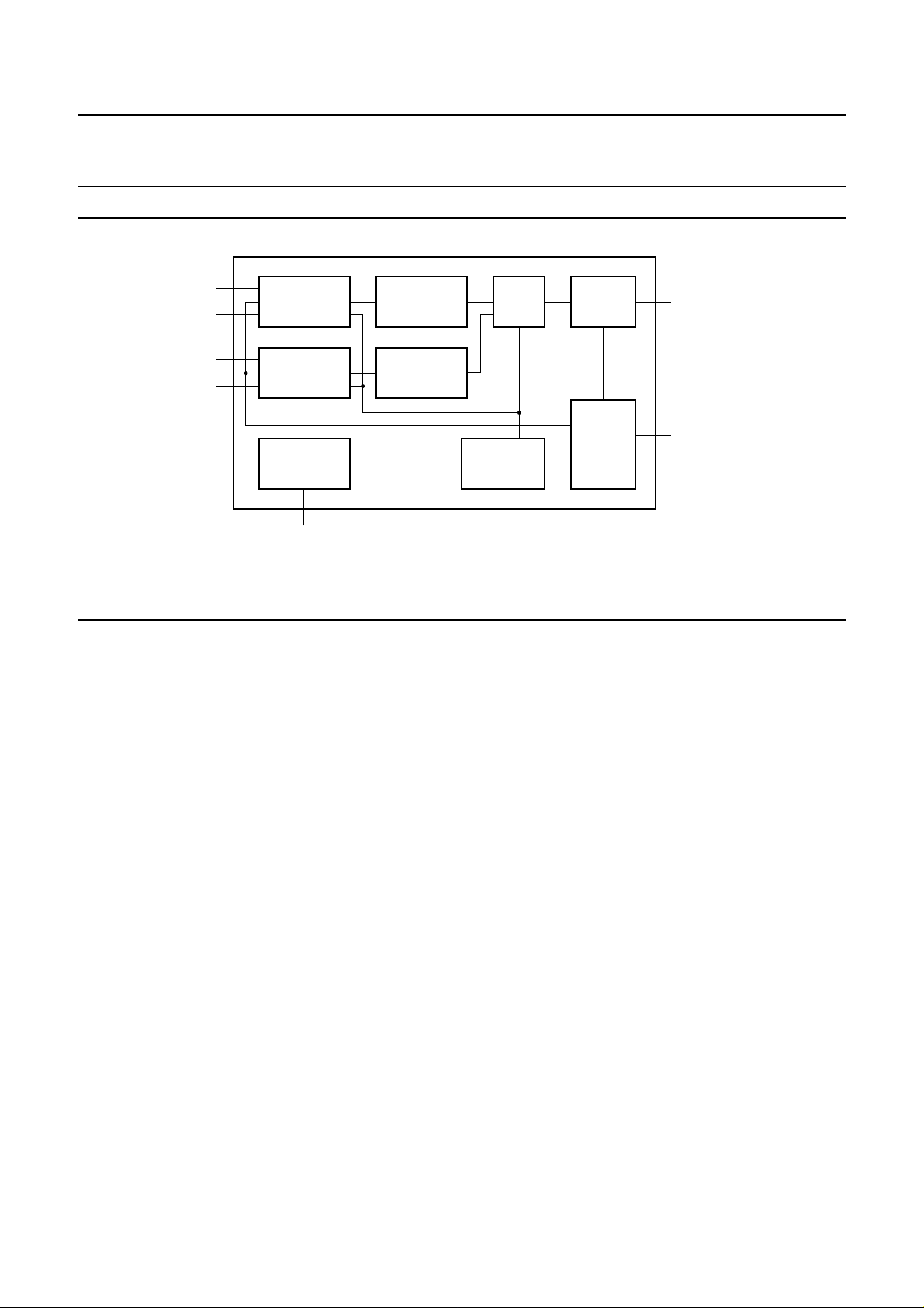
handbook, full pagewidth
+V
−V
+V
−V
O1
O1
O2
O2
ADC1
ADC2
RESET
DECIMATION
FILTER
DECIMATION
FILTER
UZZ9000
ALU DAC output
CONTROL
OSCILLATOR
angle range
offset
DATA-CLK
SMODE
reset
Fig.1 Block diagram.
The following list gives a short description of the relevant
block functions:
1. The ADC block contains two Sigma Delta AD
converters, sensor offset correction circuitry and the
circuitry required for the sensitivity and offset
adjustment of the chip output voltage curve.
2. The decimation filter block comprises two digital low
pass decimation filtersconvert the low resolution high
speed bit stream output from the ADC’s into a low
speed digital word.
3. The ALU block derives an angle value from the two
digital inputs using the CORDIC algorithm.
4. The DAC converts the output of the ALU block to an
analog signal.
5. The CONTROL block provides the clock and the
control signals for the chip.
6. The RESET block supplies a reset signal during
power-up and power-down when the power supply is
below a certain value.
7. The Oscillator generates the master clock.
MHB694
Angle range selection
In order to accommodate varying applications, both the
mechanical input angular range of the UZZ9000 and the
zeropoint oftheoutput curveareuser programmable.This
section describes how to select a desired mode.
The output curve is adjusted by changing the angular
range asshown inFig.2. Without anyzero pointoffset, the
ramp-up starts at mechanical 0° (α1=0°). When using a
KMZ41 sensor, the maximum angular range ∆α
is 0° to 180°. For the UZZ9000, smaller angular ranges
can be set. In this case, α2 becomes smaller than 180°
and the output curve is clipped at this position. The
location of discontinuity XD (change from lower to upper
clipping area) depends on the adjusted range and can be
calculated as follows:
180°∆α–
∆α
X
D
+=
-------------------------2
Inorder tocompensate fortolerances, thezero point ofthe
output curve can be shifted by ±5˚ in steps of 0.5°. The
effect of this measure is shown in Fig.3. Now α1 is no
longer identicalwith mechanical 0˚,but with the zero point
shift X
. Consequently, the location of discontinuity X
off
D
can be calculated as follows:
2000 Nov 27 5
X
Dxoff
∆α+
180°∆α–
+=
-------------------------2
 Loading...