

Philips UDA1330ATS-N1 Datasheet
DATA SH EET
Preliminary specification
Supersedes data of 1998 Mar 06
File under Integrated Circuits, IC01
1998 Mar 24
INTEGRATED CIRCUITS
UDA1330ATS
Low-cost stereo filter DAC
1998 Mar 24 2
Philips Semiconductors Preliminary specification
Low-cost stereo filter DAC UDA1330ATS
FEATURES
General
• Low power consumption
• 4.5 to 5.5 V power supply
• Selectable control via L3 microcontroller interface or via
static pin control
• System clock frequencies of 256, 384 and 512f
s
,
selectable via the L3 interface or 256fsand 384fs clock
mode selectable via the static pin control
• Supports sampling frequencies (fs) from 16 to 48 kHz
• Integrated digital filter plus non inverting
Digital-to-Analog Converter (DAC)
• No analog post filtering required for DAC
• Slave mode only applications
• Easy application
• Small package size (SSOP16).
Multiple format input interface
• I
2
S-bus, MSB-justified and LSB-justified 16, 18 and
20 bits format compatible (in L3 mode)
• I2S-bus and LSB-justified 16, 18 and 20 bits format
compatible
• 1fs input format data rate.
DAC digital sound processing
• Digital logarithmic volume control via L3 control
• Digital de-emphasis for 32, 44.1 and 48 kHz sampling
frequencies via L3 control or 44.1 kHz sampling
frequency via static pin control
• Soft mute via static pin control or via L3 interface.
Advanced audio configuration
• Stereo line output (under L3 volume control)
• High linearity, wide dynamic range, low distortion.
APPLICATIONS
• 5 V PC audio applications
• Car radio applications.
GENERAL DESCRIPTION
The UDA1330ATS is a single-chip stereo DAC employing
bitstream conversion techniques. The UDA1330ATS can
be used in two modes, either the L3 mode or the static pin
mode.
The UDA1330ATS supports the I
2
S-bus data format with
word lengths of up to 20 bits, the MSB-justified data format
with word lengths of up to 20 bits and the LSB-justified
serial data format with word lengths of 16, 18 and 20 bits.
In the L3 mode, all digital sound processing features must
be controlled via the L3 interface, including the selection of
the system clock setting.
In the two static modes, the UDA1330ATS can be
operated in the 256fs and 384fs system clock mode.
The mute, de-emphasis for 44.1 kHz and 4 digital input
formats (I2S-bus and 16, 18, and 20 bits LSB formats) can
be selected via static pins. The L3 interface cannot be
used in this application mode. Volume control is also not
available in this mode.
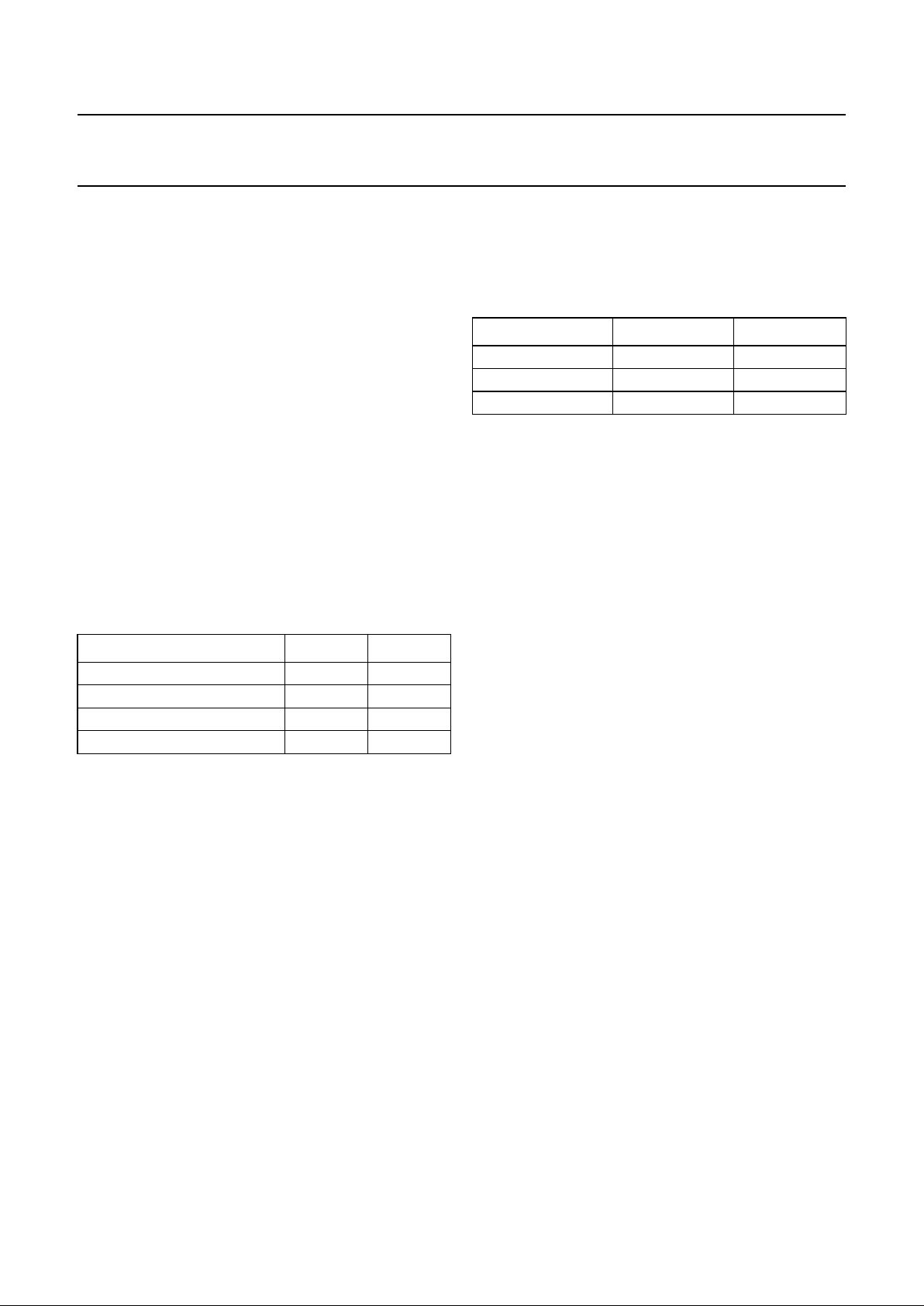
ORDERING INFORMATION
TYPE NUMBER
PACKAGE
NAME DESCRIPTION VERSION
UDA1330ATS/N1 SSOP16 plastic shrink small outline package; 16 leads; body width 4.4 mm SOT369-1
1998 Mar 24 3
Philips Semiconductors Preliminary specification
Low-cost stereo filter DAC UDA1330ATS
QUICK REFERENCE DATA
Note
1. The output voltage scales linearly with the power supply voltage.
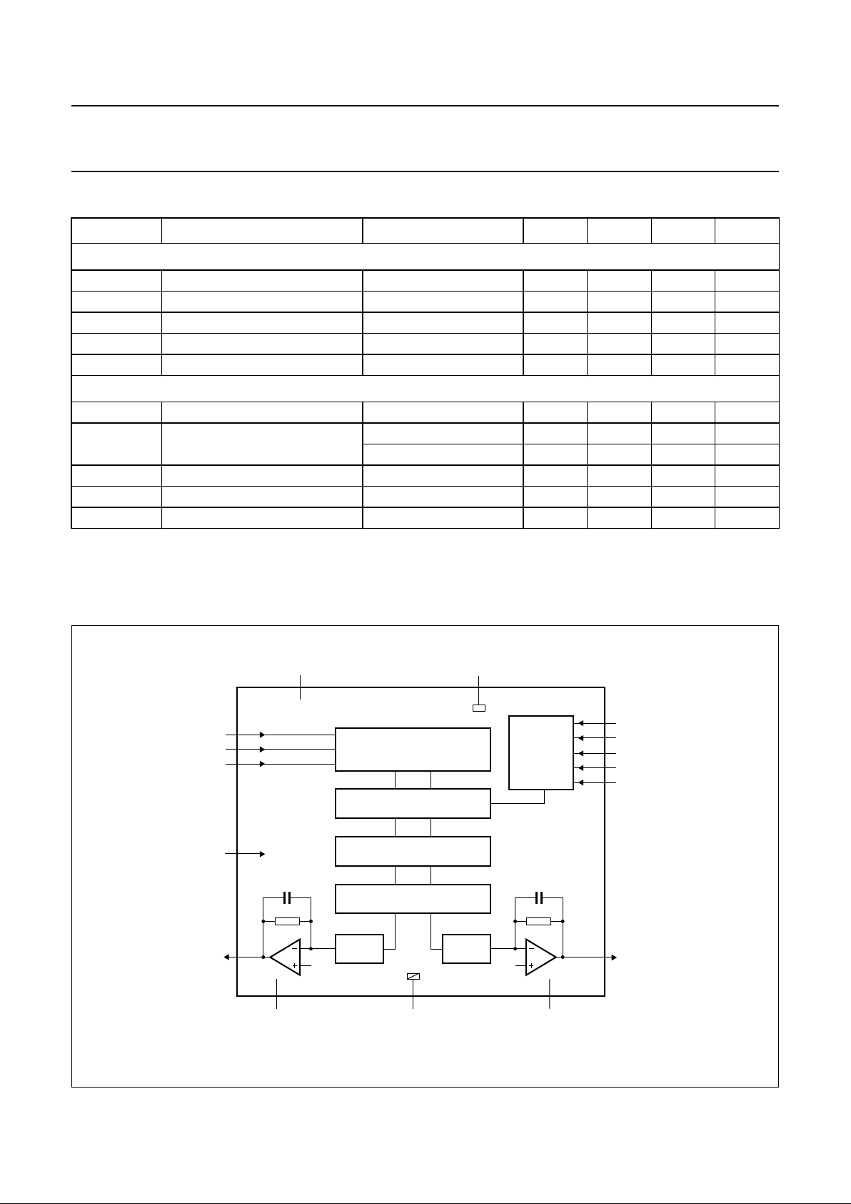
BLOCK DIAGRAM
SYMBOL PARAMETER CONDITIONS MIN. TYP. MAX. UNIT
Supplies
V
DDA
analog supply voltage 4.5 5.0 5.5 V
V
DDD
digital supply voltage 4.5 5.0 5.5 V
I
DDA
DAC supply current − 9.5 − mA
I
DDD
digital supply current − 5.5 − mA
T
amb
operating ambient temperature −20 − +85 °C
DAC
V
o(rms)
output voltage (RMS value) note 1 − 1.45 − V
(THD + N)/S total harmonic distortion plus
noise-to-signal ratio
at 0 dB −−88 −83 dB
at −60 dB; A-weighted −−40 −35 dB
S/N signal-to-noise ratio code = 0; A-weighted − 100 −95 dB
α
cs
channel separation − 100 − dB
T
amb
operating ambient temperature −20 − +85 °C
Fig.1 Block diagram.
handbook, full pagewidth
MGL401
DAC
UDA1330ATS
NOISE SHAPER
INTERPOLATION FILTER
VOLUME/MUTE/DE-EMPHASIS
CONTROL
INTERFACE
14
15
DAC
6
DIGITAL INTERFACE
8
16
9
10
3
2
1
4
5
11
7
13 12
V
O(R)
BCK
V
SSA
WS
V
O(L)
DATAI
V
DDA
V
DDD
V
ref(DAC)
V
SSD
APPL0
SYSCLK
APPL1
APPSEL
APPL2
APPL3
1998 Mar 24 4
Philips Semiconductors Preliminary specification
Low-cost stereo filter DAC UDA1330ATS
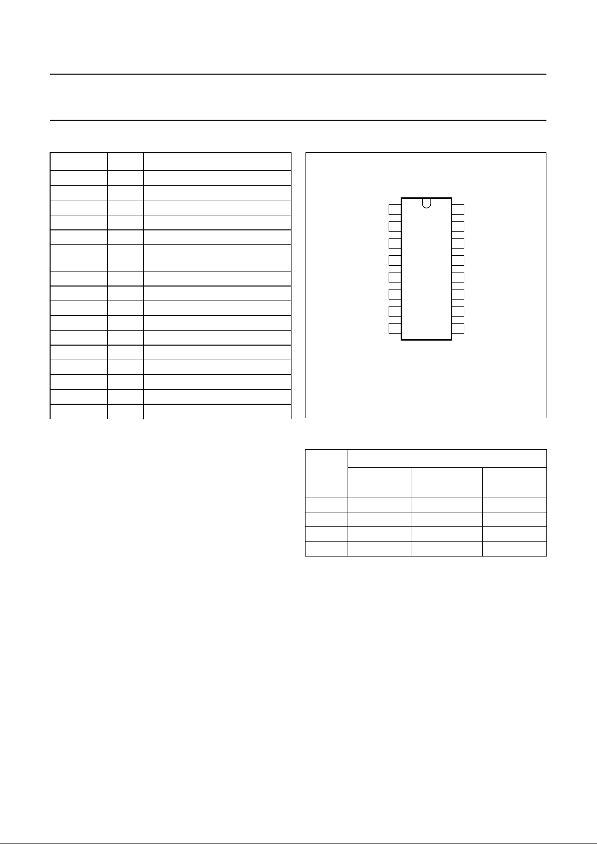
PINNING
SYMBOL PIN DESCRIPTION
BCK 1 bit clock input
WS 2 word select input
DATAI 3 data input
V
DDD
4 digital power supply
V
SSD
5 digital ground
SYSCLK 6 system clock input 256, 384
and 512f
s
APPSEL 7 application mode select input
APPL3 8 application input pin 3
APPL2 9 application input pin 2
APPL1 10 application input pin 1
APPL0 11 application input pin 0
V
ref(DAC)
12 DAC reference voltage
V
DDA
13 analog supply voltage
V
O(L)
14 left output voltage
V
SSA
15 analog ground
V
O(R)
16 right output voltage
Fig.2 Pin configuration.
handbook, halfpage
UDA1330ATS
MGL402
1
2
3
4
5
6
7
8
16
15
14
13
12
11
10
9
V
O(R)
BCK
V
SSA
WS
V
O(L)
DATAI
V
DDA
V
DDD
V
ref(DAC)
V
SSD
APPL0SYSCLK
APPL1APPSEL
APPL2APPL3
FUNCTIONAL DESCRIPTION
System clock
The UDA1330ATS operates in slave mode only. In all
applications, therefore, the system devices must provide
the system clock. The system frequency is selectable and
depends on the mode of operation.
The options are 256, 384 and 512f
s
for the L3 mode and
256fs plus 384fs for the static mode. The system clock
must be locked in frequency to the digital interface input
signals.
The UDA1330ATS supports sampling frequencies from
16 to 48 kHz.
Application modes
Operation can be set with the tri-value APPSEL pin, to
L3 mode (APPSEL = V
SSD
) or to either of two static modes
(APPSEL = 0.5V
DDD
or APPSEL = V
DDD
), see Table 1 for
APPL0 to APPL3 pin functions (active = HIGH).
Table 1 Selection modes via APPSEL
For example, in static pin control mode, the output signal
can be soft muted by setting APPL0 HIGH. De-emphasis
can be switched on for 44.1 kHz by setting APPL1 HIGH.
APPL1 LOW will disable de-emphasis.
It should be noted that when the L3 interface is used, an
L3 initialisation must be done when the IC is powered up.
PIN
APPSEL
V
SSD
0.5V
DDD
(384fs)
V
DDD
(256fs)
APPL0 TEST MUTE MUTE
APPL1 L3CLOCK DEEM DEEM
APPL2 L3MODE SF0 SF0
APPL3 L3DATA SF1 SF1
1998 Mar 24 5
Philips Semiconductors Preliminary specification
Low-cost stereo filter DAC UDA1330ATS
Multiple format input interface
L3
MODE
• I2S-bus with data word length of up to 20 bits
• MSB-justified format with data word length up to 20 bits
• LSB-justified format with data word length of
16, 18 or 20 bits.
S
TATIC PIN MODE
The UDA1330ATS supports the following data input name
formats in the static pin mode (via SF0 and SF1):
• I2S-bus with data word length of up to 20 bits
• LSB-justified format with data word length of
16, 18 or 20 bits.
See Table 2, for the static pin codes of the 4 formats,
selectable via SF0 and SF1.
The UDA1330ATS also accepts double speed data for
double speed data monitoring purposes.
Table 2 Input format selection using SF0 and SF1
The formats are illustrated in Fig.3. Left and right
data-channel words are time multiplexed. The WS signal
must have a 50% duty factor for all LSB-justified modes.
For the digital data interface the bit clock frequency should
be less than or equal to 64 times the word frequency;
f
BCK
= ≤ 64fWS.
Pin compatibility
In L3 interface mode the UDA1330ATS can be used on
boards that are designed for the UDA1320ATS.
IMPORTANT: It should be noted that the UDA1330ATS is
designed for 5 V operation while the UDA1320ATS is
designed for 3 V operation.
FORMAT SF0 SF1
I
2
S-bus 0 0
LSB-justified 16 bits 0 1
LSB-justified 18 bits 1 0
LSB-justified 20 bits 1 1
Interpolation filter (DAC)
The digital filter interpolates from 1 to 128fs by cascading
a recursive filter and an FIR filter, see Table 3.
Table 3 Interpolation filter characteristics
Noise shaper
The 3rd-order noise shaper operates at 128f
s
. It shifts
in-band quantization noise to frequencies well above the
audio band. This noise shaping technique enables high
signal-to-noise ratios to be achieved. The noise shaper
output is converted into an analog signal using a
Filter-Stream DAC (FSDAC).
Filter stream DAC
The FSDAC is a semi-digital reconstruction filter that
converts the 1-bit data stream of the noise shaper to be
analog output voltage. The filter coefficients are
implemented as current sources and are summed at
virtual ground of the output operational amplifier. In this
way very high signal-to-noise performance and low clock
jitter sensitivity is achieved. A post-filter is not needed due
to the inherent filter function of the DAC. On-board
amplifiers convert the FSDAC output current to an output
voltage signal capable of driving a line output.
The output voltage scales linearly with the power supply
voltage.
ITEM CONDITION VALUE (dB)
Pass-band ripple 0 to 0.45f
s
±0.1
Stop band >0.55f
s
−50
Dynamic range 0 to 0.45f
s
108

1998 Mar 24 6
Philips Semiconductors Preliminary specification
Low-cost stereo filter DAC UDA1330ATS
This text is here in white to force landscape pages to be rotated correctly when browsing through the pdf in the Acrobat reader.This text is here in
_white to force landscape pages to be rotated correctly when browsing through the pdf in the Acrobat reader.This text is here inThis text is here in
white to force landscape pages to be rotated correctly when browsing through the pdf in the Acrobat reader. white to force landscape pages to be ...
n
dbook, full pagewidth
LSB-JUSTIFIED FORMAT 16 BITS
LSB-JUSTIFIED FORMAT 18 BITS
LSB-JUSTIFIED FORMAT 20 BITS
MSB-JUSTIFIED FORMAT
WS
LEFT
LEFT
LEFT
LEFT
RIGHT
RIGHT
RIGHT
RIGHT
32
2
215161718 1
1516 1
1321
MSB B2 MSBLSB LSB MSB B2B2
MSB LSBB2
MSB B2 B3 B4
B15
LSB
B17
215161718 1
MSB B2 B3 B4
LSB
B17
2151617181920 1
MSB B2 B3 B4 B5 B6
LSB
B19
2151617181920 1
MSB B2 B3 B4 B5 B6
LSB
B19
21516 1
MSB LSBB2 B15
≥8 ≥8
BCK
DATAI
WS
LEFT
RIGHT
321321
MSB B2 MSBLSB LSB MSBB2
≥8 ≥8
BCK
DATAI
WS
BCK
DATAI
WS
BCK
DATAI
WS
BCK
DATAI
INPUT FORMAT I
2
S-BUS
MBK071
Fig.3 Serial interface; input format I2S-bus.
 Loading...