

Philips UDA1330ATS Datasheet
INTEGRATED CIRCUITS
DATA SH EET
UDA1330ATS
Low-cost stereo filter DAC
Product specification
Supersedes data of 2000 April 18
File under Integrated Circuits, IC01
2001 Feb 02

Philips Semiconductors Product specification
Low-cost stereo filter DAC UDA1330ATS
FEATURES
General
• Low power consumption
• Power supply voltage from 2.7 to 5.5 V
• Selectable controlvia L3 microcontroller interface or via
static pin control
• System clock frequencies of 256fs, 384fsand 512f
selectable via L3 interface or 256fsand 384fs via static
pin control
• Supports sampling frequencies (fs) from 8 to 55 kHz
• Integrated digital filter plus non inverting
Digital-to-Analog Converter (DAC)
• No analog post filtering required for DAC
• Slave mode only applications
• Easy application
• Small package size (SSOP16)
• TTL tolerant input pads
• Pin and function compatible with the UDA1320ATS.
Multiple format input interface
• L3 mode: I2S-bus, MSB-justified or LSB-justified
16, 18 and 20 bits format compatible
• Static pin mode: I2S-bus and LSB-justified
16, 18 and 20 bits format compatible
• 1fsinput format data rate.
DAC digital sound processing
• Digital logarithmic volume control in L3 mode
• Digital de-emphasis for 32, 44.1 and 48 kHz sampling
frequenciesinL3 mode or 44.1 kHz sampling frequency
in static pin mode
• Soft mute control both in static pin mode and L3 mode.
s
APPLICATIONS
• PC audio applications
• Car radio applications.
GENERAL DESCRIPTION
The UDA1330ATS is a single-chip stereo DAC employing
bitstream conversion techniques.
The UDA1330ATS supports the I2S-bus data format with
wordlengths of upto20 bits, the MSB-justified dataformat
with word lengths of up to 20 bits and the LSB-justified
serial data format with word lengths of 16, 18 and 20 bits.
The UDA1330ATS canbe used in two modes: L3 mode or
the static pin mode.
In the L3 mode, all digital sound processing features must
becontrolled via the L3 interface, includingtheselectionof
the system clock setting.
In the two static modes, the UDA1330ATS can be
operated in the 256fsand 384fs system clock mode.
Muting, de-emphasis for 44.1 kHz and four digital input
formats (I2S-bus or LSB-justified 16, 18, and 20 bits) can
be selected via static pins. The L3 interface cannot be
used in this application mode, so volume control is not
available in this mode.
Advanced audio configuration
• Stereo line output (volume control in L3 mode)
• High linearity, wide dynamic range and low distortion.
ORDERING INFORMATION
TYPE NUMBER
NAME DESCRIPTION VERSION
UDA1330ATS SSOP16 plastic shrink small outline package; 16 leads; body width 4.4 mm SOT369-1
2001 Feb 02 2
PACKAGE
Philips Semiconductors Product specification
Low-cost stereo filter DAC UDA1330ATS
QUICK REFERENCE DATA
SYMBOL PARAMETER CONDITIONS MIN. TYP. MAX. UNIT
Supplies
V
DDA
V
DDD
I
DDA
I
DDD
T
amb
Digital-to-analog converter (V
V
o(rms)
(THD + N)/S total harmonic distortion-plus-noise to
S/N signal-to-noise ratio code = 0; A-weighted − 100 95 dB
α
cs
Digital-to-analog converter (V
V
o(rms)
(THD + N)/S total harmonic distortion-plus-noise to
S/N signal-to-noise ratio code = 0; A-weighted − 100 − dB
α
cs
Power dissipation
P power dissipation playback mode
DAC analog supply voltage 2.7 5.0 5.5 V
digital supply voltage 2.7 5.0 5.5 V
DAC analog supply current V
DDA
= 5.0 V
operating − 9.5 − mA
power-down − 400 −µA
V
= 3.3 V
DDA
operating − 7.0 − mA
power-down − 250 −µA
digital supply current V
= 5.0 V − 5.5 − mA
DDD
V
= 3.3 V − 3.0 − mA
DDD
ambient temperature −40 − +85 °C
DDA=VDDD
= 5.0 V)
output voltage (RMS value) note 1 − 1.45 − V
at 0 dB −−90 −85 dB
signal ratio
at −60 dB; A-weighted −−40 −35 dB
channel separation − 100 − dB
DDA=VDDD
= 3.3 V)
output voltage (RMS value) note 1 − 1.0 − V
at 0 dB −−85 − dB
signal ratio
at −60 dB; A-weighted −−38 − dB
channel separation − 100 − dB
V
DDA=VDDD
V
DDA=VDDD
= 5.0 V − 75 − mW
= 3.3 V − 33 − mW
Note
1. The output voltage scales linearly with the power supply voltage.
2001 Feb 02 3
Philips Semiconductors Product specification
Low-cost stereo filter DAC UDA1330ATS
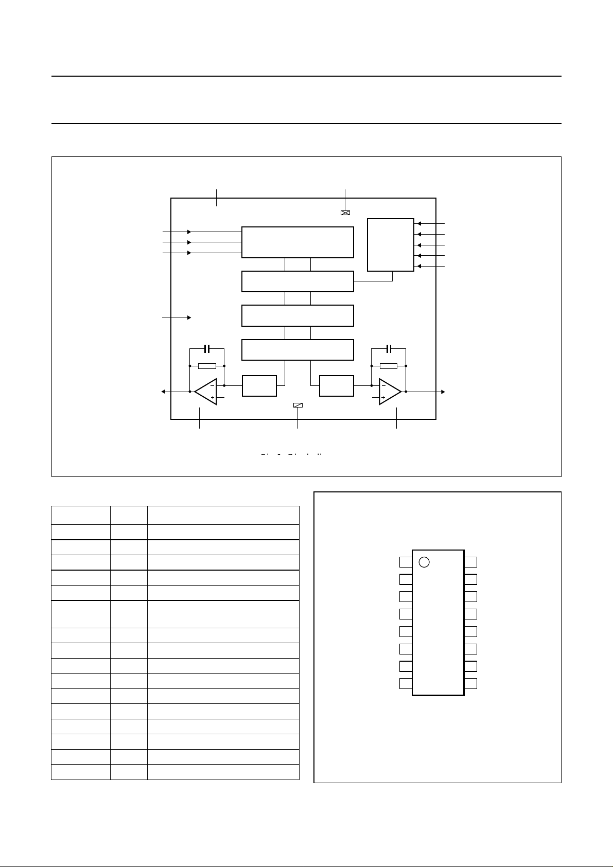
BLOCK DIAGRAM
handbook, full pagewidth
BCK
WS
DATAI
SYSCLK
VOUTL
V
DDD
4
1
2
3
UDA1330ATS
6
14
13 12
V
DDA
DIGITAL INTERFACE
VOLUME/MUTE/DE-EMPHASIS
INTERPOLATION FILTER
NOISE SHAPER
DAC
15
V
SSA
Fig.1 Block diagram.
Fig.0 Block diagram.
V
DAC
SSD
5
CONTROL
INTERFACE
V
ref(DAC)
7
APPSEL
11
APPL0
10
APPL1
9
APPL2
8
APPL3
16
VOUTR
MGL401
PINNING
SYMBOL PIN DESCRIPTION
BCK 1 bit clock input
WS 2 word select input
DATAI 3 data input
V
DDD
V
SSD
SYSCLK 6 system clock input: 256f
4 digital supply voltage
5 digital ground
and 512f
s
, 384f
s
APPSEL 7 application mode select input
APPL3 8 application input 3
APPL2 9 application input 2
APPL1 10 application input 1
APPL0 11 application input 0
V
ref(DAC)
V
DDA
12 DAC reference voltage
13 analog supply voltage for DAC
VOUTL 14 left channel output
V
SSA
15 analog ground
VOUTR 16 right channel output
handbook, halfpage
s
WS
DATAI
V
DDD
V
SSD
1
2
3
4
UDA1330ATS
5
6
7
8
MGL402
16
15
14
13
12
11
10
9
VOUTRBCK
V
SSA
VOUTL
V
DDA
V
ref(DAC)
APPL0SYSCLK
APPL1APPSEL
APPL2APPL3
Fig.2 Pin configuration.
2001 Feb 02 4
Philips Semiconductors Product specification
Low-cost stereo filter DAC UDA1330ATS
FUNCTIONAL DESCRIPTION
System clock
The UDA1330ATS operates in slave mode only.
Therefore, in all applications the system devices must
provide the system clock. The system frequency (f
sys
) is
selectable and depends on the application mode. The
options are: 256fs, 384fsand 512fs for the L3 mode and
256fsor 384fs for the static pin mode. The system clock
must be locked in frequency to the digital interface input
signals.
The UDA1330ATS supports sampling frequencies from
8 to 55 kHz.
Application modes
The application mode can be set with the three-level
pin APPSEL (see Table 1):
• L3 mode
• Static pin mode with f
• Static pin mode with f
sys
sys
= 384f
= 256fs.
s
Table 1 Selecting application mode and system clock
frequency via pin APPSEL
In the L3 mode, pin APPL0 must be set to LOW. It should
be noted that when the L3 mode is used, an initialization
must be performed when the IC is powered-up.
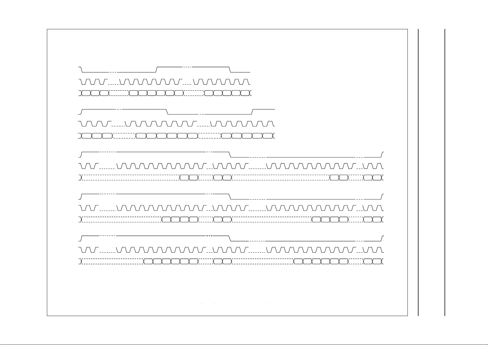
Multiple format input interface
D
ATA FORMATS
Thedigitalinterface of the UDA1330ATS supportsmultiple
format inputs (see Fig.3).
Left and right data-channel words are time multiplexed.
The WS signal must have a 50% duty factor for all
LSB-justified formats.
The BCK clock can be up to 64fs, or in other words the
BCK frequency is 64 times the Word Select (WS)
frequency or less: f
≤ 64 × fWS.
BCK
Important: the WS edge MUST fall on the negative edge
of the BCK at all times for proper operation of the digital
interface.
The UDA1330ATS also accepts double speed data for
double speed data monitoring purposes
L3 MODE
VOLTAGE ON
PIN APPSEL
V
SSD
0.5V
DDD
V
DDD
MODE f
sys
L3 mode 256fs, 384fsor 512f
static pin mode
384f
256f
s
s
The function of an application input pin (active HIGH)
depends on the application mode (see Table 2).
Table 2 Functions of application input pins
FUNCTION
PIN
L3 MODE STATIC PIN MODE
APPL0 TEST MUTE
APPL1 L3CLOCK DEEM
APPL2 L3MODE SF0
APPL3 L3DATA SF1
For example, in the static pin mode the output signal can
be soft muted by setting pin APPL0 to HIGH.
De-emphasis can be switched on for 44.1 kHz by setting
pin APPL1to HIGH; setting pin APPL1to LOW will disable
de-emphasis.
This mode supports the following input formats:
• I2S-bus format with data word length of up to 20 bits
s
• MSB-justified format with data word length up to 20 bits
• LSB-justified format with data word length of
16, 18 or 20 bits.
STATIC PIN MODE
This mode supports the following input formats:
• I2S-bus format with data word length of up to 20 bits
• LSB-justified format with data word length of
16, 18 or 20 bits.
These four formats are selectable via the static pin codes
SF0 and SF1 (see Table 3).
Table 3 Input format selection using SF0 and SF1
FORMAT SF0 SF1
2
I
S-bus 0 0
LSB-justified 16 bits 0 1
LSB-justified 18 bits 1 0
LSB-justified 20 bits 1 1
2001 Feb 02 5
Philips Semiconductors Product specification
Low-cost stereo filter DAC UDA1330ATS
Interpolation filter (DAC)
Thedigital filter interpolates from1fsto 128fsbycascading
a recursive filter and an FIR filter (see Table 4).
Table 4 Interpolation filter characteristics
ITEM CONDITION VALUE (dB)
Pass-band ripple 0 to 0.45f
Stop band >0.55f
Dynamic range 0 to 0.45f
s
s
s
±0.1
−50
108
Noise shaper
The 3rd-order noise shaper operates at 128f
. It shifts
s
in-band quantization noise to frequencies well above the
audio band. This noise shaping technique enables high
signal-to-noise ratios to be achieved. The noise shaper
output is converted into an analog signal using a Filter
Stream DAC (FSDAC).
Filter stream DAC
The FSDAC is a semi-digital reconstruction filter that
converts the 1-bit data stream of the noise shaper to an
analog output voltage. The filter coefficients are
implemented as current sources and are summed at
virtual ground of the output operational amplifier. In this
way very high signal-to-noise performance and low clock
jitter sensitivity is achieved. A post-filter is not needed due
to the inherent filter function of the DAC. On-board
amplifiers convert the FSDAC output current to an output
voltage signal capable of driving a line output.
The output voltage of the FSDAC scales linearly with the
power supply voltage.
Pin compatibility
In the L3 mode the UDA1330ATS can be used on boards
that are designed for the UDA1320ATS.
Remark: It should be noted that the UDA1330ATS is
designed for 5 V operation while the UDA1320ATS is
designed for 3 V operation. This means that the
UDA1330ATS can be used with the UDA1320ATS supply
voltage range, but the UDA1320ATS can not beused with
the 5 V supply voltage.
2001 Feb 02 6
This text is here in white to force landscape pages to be rotated correctly when browsing through the pdf in the Acrobat reader.This text is here in
o
_white to force landscape pages to be rotated correctly when browsing through the pdf in the Acrobat reader.This text is here inThis text is here in
white to force landscape pages to be rotated correctly when browsing through the pdf in the Acrobat reader. white to force landscape pages to be ...
2001 Feb 02 7
ok, full pagewidth
Philips Semiconductors Product specification
Low-cost stereo filter DAC UDA1330ATS
LEFT
LEFT
2
I
MSB-JUSTIFIED FORMAT
LEFT
LEFT
WS
BCK
DATA
WS
BCK
DATA
WS
BCK
DATA
WS
BCK
DATA
MSB B2
MSB B2 MSBLSB LSB MSB B2B2
RIGHT
3
21> = 812 3
MSB MSBB2
S-BUS FORMAT
RIGHT
> = 8 > = 8
MSB B2 B3 B4
321321
16
15 2 1
MSB
B2
16
1518 17 2 1
> = 8
B15
LSB
LSB-JUSTIFIED FORMAT 16 BITS
B17
LSB
LSB-JUSTIFIED FORMAT 18 BITS
RIGHT
RIGHT
16
MSB B2
16 1518 17 2 1
MSB B2 B3 B4
15 2 1
B15 LSB
B17 LSB
WS
BCK
DATA
LEFT
16
MSB B2 B3 B4 B5 B6
Fig.3 Digital interface input format data format.Fig.0 Digital interface input format data format.
1518 1720 19 2 1
B19
LSB
LSB-JUSTIFIED FORMAT 20 BITS
RIGHT
16
MSB B2 B3 B4 B5 B6
1518 1720 19 2 1
B19 LSB
MBL140

Philips Semiconductors Product specification
Low-cost stereo filter DAC UDA1330ATS
L3 INTERFACE
The following system and digital sound processing
features can be controlled in the L3 mode of the
UDA1330ATS:
• System clock frequency
• Data input format
• De-emphasis for 32, 44.1 and 48 kHz
• Volume
• Soft mute.
Theexchange of dataand control information betweenthe
microcontroller and the UDA1330ATS is accomplished
through a serial interface comprising the following signals:
• L3DATA
• L3MODE
• L3CLOCK.
Information transfer through the microcontroller bus is
organized in accordance with the L3 interface format, in
which two different modes of operation can be
distinguished: address mode and data transfer mode.
Address mode
The address mode (see Fig.4) is required to select a
device communicating via the L3 interface and to define
the destination registers for the data transfer mode.
Data bits 7 to 2 represent a 6-bit device address where
bit 7 is the MSB. The address of the UDA1330ATS is
000101 (bit 7 to bit 2). If the UDA1330ATS receives a
different address, it will deselect its microcontroller
interface logic.
Data transfer mode
The fundamental timing of data transfers (see Fig.5) is
essentially the same as the address mode. The maximum
input clock frequency and data rate is 64fs.
Data transfer can only be in one direction, consisting of
input to the UDA1330ATS to program sound processing
andother functional features. Alldatatransfersare by 8-bit
bytes. Data will be stored in the UDA1330ATS after
reception of a complete byte.
A multibyte transfer is illustrated in Fig.6.
Registers
The sound processing and other feature values are stored
inindependent registers. The first selectionoftheregisters
is achieved by the choice of data type that is transferred.
Thisis performed intheaddress mode usingbit 1 and bit 0
(see Table 5).
Table 5 Selection of data transfer
BIT 1 BIT 0 TRANSFER
0 0 data (volume, de-emphasis, mute)
0 1 not used
1 0 status (system clock frequency,
data input format)
1 1 not used
The second selection is performed by the 2 MSBs of the
data byte (bit 7 and bit 6). The other bits in the data byte
(bit 5 to bit 0) represent the value that is placed in the
selected registers.
The ‘status’ settings are given in Table 6 and the ‘data’
settings are given in Table 7.
The selected address remains active during subsequent
data transfers until the UDA1330ATS receives a new
address command.
2001 Feb 02 8
 Loading...