

Philips UDA1328T Datasheet
INTEGRATED CIRCUITS
DATA SH EET
UDA1328T
Multi-channel filter DAC
Preliminary specification
File under Integrated Circuits, IC01
1999 Oct 12

Philips Semiconductors Preliminary specification
Multi-channel filter DAC UDA1328T
CONTENTS
1 FEATURES
1.1 General
1.2 Multiple format input interface
1.3 Multi-channel DAC
1.4 Advanced audio configuration
2 APPLICATIONS
3 GENERAL DESCRIPTION
4 ORDERING INFORMATION
5 QUICK REFERENCE DATA
6 BLOCK DIAGRAM
7 PINNING
8 FUNCTIONAL DESCRIPTION
8.1 System clock
8.2 Application modes
8.3 Interpolation filter (DAC)
8.4 Digital silence detection
8.5 Noise shaper
8.6 Filter Stream DAC
8.7 Static Mode
8.7.1 System clock setting
8.7.2 De-emphasis control
8.7.3 Digital interface formats
8.8 L3 mode
8.8.1 Digital interface formats
8.8.2 L3 address
9 L3 INTERFACE DESCRIPTION
9.1 Address mode
9.2 Data transfer mode
9.2.1 Programming the sound processing and other
features
9.2.2 Reset bit
9.2.3 System clock frequency
9.2.4 Data input format
9.2.5 Quick mute
9.2.6 Power control
9.3 Feature settings
9.3.1 Volume control
9.3.2 Sub volume control
9.3.3 Mute
9.3.4 Digital silence mode
9.3.5 De-emphasis
9.3.6 Output polarity control
10 LIMITING VALUES
11 HANDLING
12 THERMAL CHARACTERISTICS
13 QUALITY SPECIFICATION
14 DC CHARACTERISTICS
15 AC CHARACTERISTICS (ANALOG)
16 AC CHARACTERISTICS (DIGITAL)
17 APPLICATION INFORMATION
18 PACKAGE OUTLINE
19 SOLDERING
19.1 Introduction to soldering surface mount
packages
19.2 Reflow soldering
19.3 Wave soldering
19.4 Manual soldering
19.5 Suitability of surface mount IC packages for
wave and reflow soldering methods
20 DEFINITIONS
21 LIFE SUPPORT APPLICATIONS
1999 Oct 12 2
Philips Semiconductors Preliminary specification
Multi-channel filter DAC UDA1328T
1 FEATURES
1.1 General
• 2.7 to 3.6 V power supply
• 5 V tolerant TTL compatible inputs
• Selectable controlvia L3 microcontroller interface or via
static pin control
• Multi-channel integrated digital filter plus non-inverting
Digital-to-Analog Converter (DAC)
• Supports sample frequencies between 5 and 100 kHz
• Digital silence detection (output)
• Slave mode only applications
• No analog post filtering required for DAC
• Easy application.
2 APPLICATIONS
This multi-channel DAC is eminently suitable for DVD like
applications in which 5.1 channel encoded signals are
used.
3 GENERAL DESCRIPTION
1.2 Multiple format input interface
• I2S-bus, MSB-justified and LSB-justified format
compatible (in L3 mode)
• I2S-bus and LSB-justified format compatible
• 1fs input format data rate.
1.3 Multi-channel DAC
• 6-channel DAC with power on/off control
• Digital logarithmic volume control via L3; volume can be
set for each of the channels individually
• Digital de-emphasis for 32, 44.1, 48 and 96 kHz fs via
L3 and, for 32, 44.1 and 48 kHz in static mode
• Soft or quick mute via L3
• Output signal polarity control via L3 microcontroller
interface.
1.4 Advanced audio configuration
• 6-channel line output (under L3 volume control)
• Astereodifferentialoutput(channel 1and channel 2) for
improved performance
• High linearity, wide dynamic range, low distortion.
The UDA1328 is a single-chip 6-channel DAC employing
bitstreamconversiontechniques,whichcanbe used either
in L3 microcontroller mode or in static pin mode.
The UDA1328 supports the I2S-bus data format with word
lengths of up to 24 bits, the MSB-justified data format with
word lengths of up to 24 bits and the LSB-justified serial
data format with word lengths of 16, 18, 20 and 24 bits.
Alldigital sound processing features canbecontrolledwith
the L3 interface e.g. volume control, selecting digital
silence type, output polarity control andmute. Also system
features such as power control, digital silence detection
mode and output polarity control.
Under static pin control, via static pins, the system clock
can be set to either 256fsor 384fs support, digital
de-emphasis can be set, there is digital mute and the
digital input formats can also be set.
4 ORDERING INFORMATION
TYPE
NUMBER
UDA1328T SO32 plastic small outline package; 32 leads; body width 7.5 mm SOT287-1
1999 Oct 12 3
NAME DESCRIPTION VERSION
PACKAGE
Philips Semiconductors Preliminary specification
Multi-channel filter DAC UDA1328T
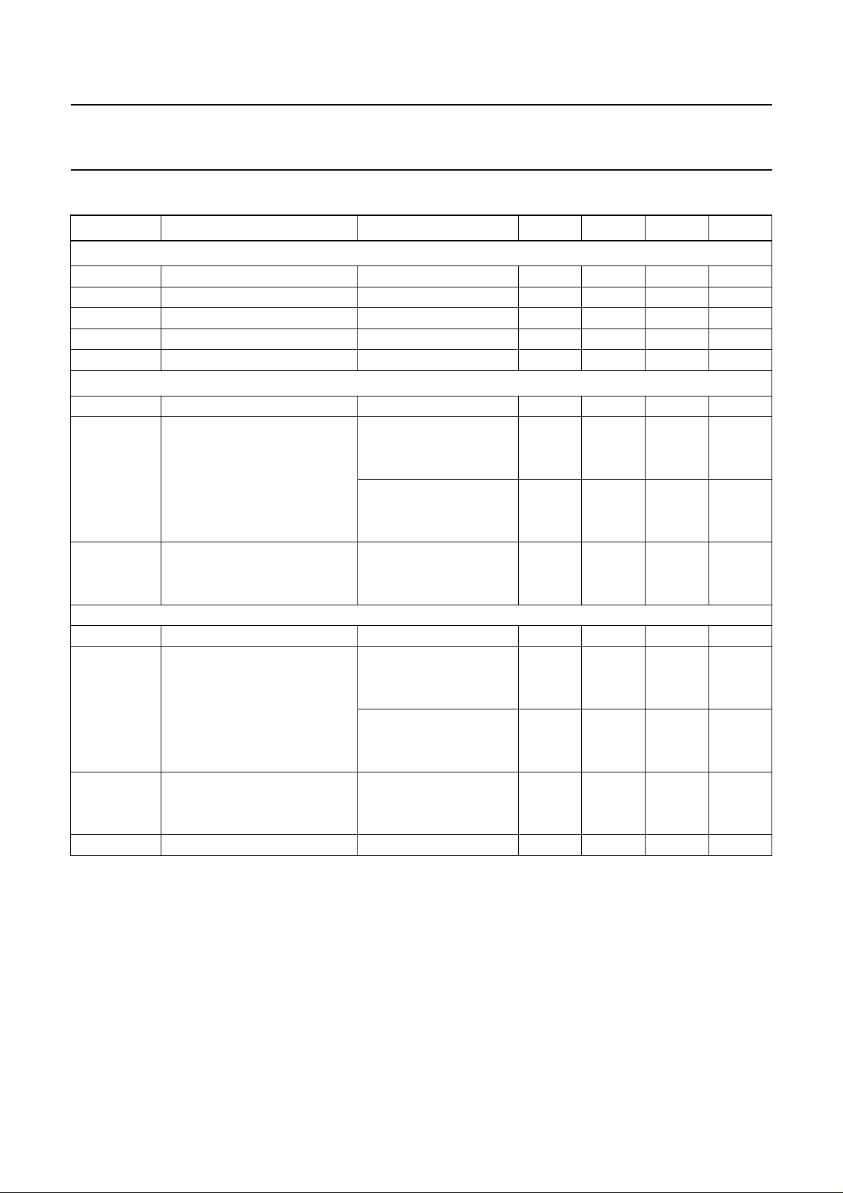
5 QUICK REFERENCE DATA
SYMBOL PARAMETER CONDITIONS MIN. TYP. MAX. UNIT
Supplies
V
DDA
V
DDD
I
DDA
I
DDD
T
amb
DAC: channels 1 and 2 differential
V
o(rms)
(THD + N)/S total harmonic distortion plus
S/N signal-to-noise ratio code = 0; A-weighted
DAC: channels 3 to 6 (channels 1 and 2 non-differential)
V
o(rms)
(THD + N)/S total harmonic distortion plus
S/N signal-to-noise ratio code = 0; A-weighted
α
cs
analog supply voltage 2.7 3.3 3.6 V
digital supply voltage 2.7 3.3 3.6 V
analog supply current 6 channels active − 28 − mA
digital supply current − 11 − mA
ambient temperature −20 − +85 °C
output voltage (RMS value) notes 1 and 2 − 2 − V
at 0 dB
noise-to-signal ratio
fs=48kHz −−95 −88 dB
f
=96kHz −−90 − dB
s
at −60 dB; A-weighted
f
=48kHz −−46 − dB
s
=96kHz −−44 − dB
f
s
f
=48kHz − 106 − dB
s
f
=96kHz − 104 − dB
s
output voltage (RMS value) note 1 − 1 − V
at 0 dB
noise-to-signal ratio
fs=48kHz −−90 −83 dB
f
=96kHz −−85 − dB
s
at −60 dB; A-weighted
f
=48kHz −−43 − dB
s
f
=96kHz −−41 − dB
s
fs=48kHz − 103 − dB
f
=96kHz − 101 − dB
s
channel separation − 100 − dB
Notes
1. The output voltage scales proportionally with the power supply voltage.
2. In this case the two outputs per channel (for channels 1 and 2) are combined.
1999 Oct 12 4
Philips Semiconductors Preliminary specification
Multi-channel filter DAC UDA1328T
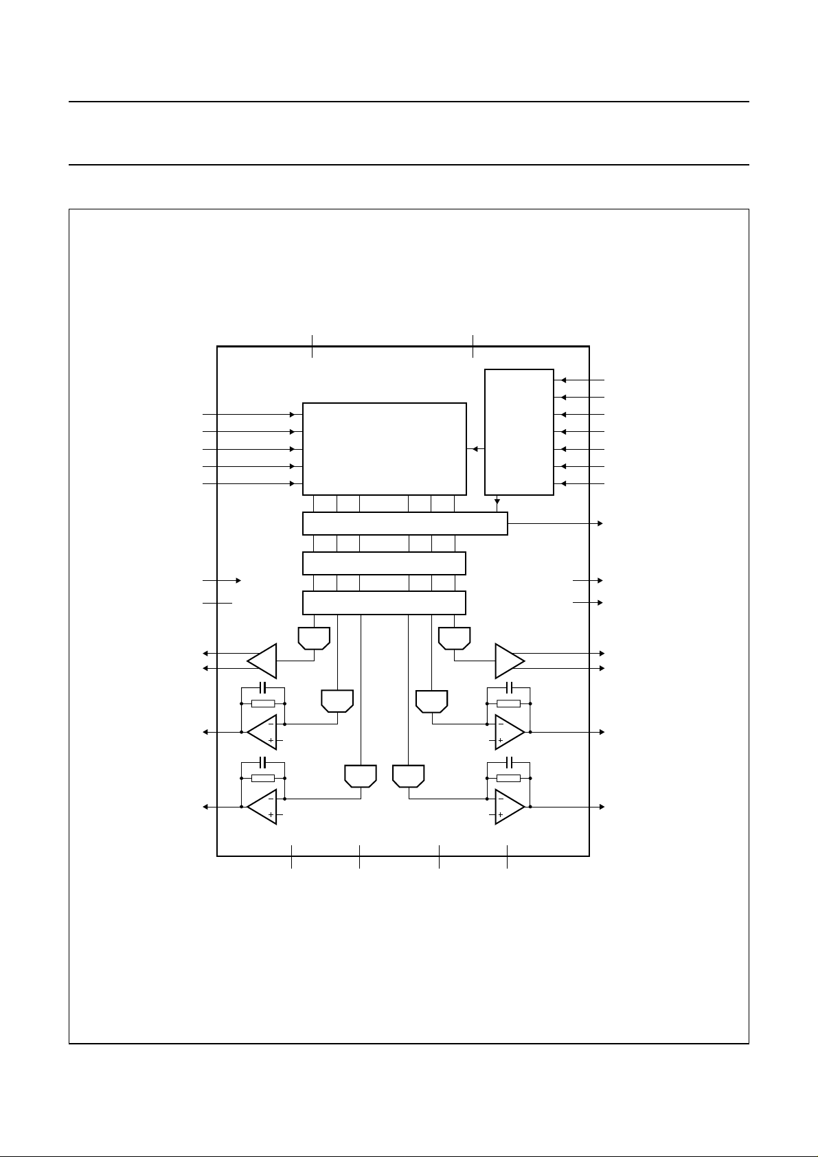
6 BLOCK DIAGRAM
handbook, full pagewidth
BCK
WS
DATAI12
DATAI34
DATAI56
TEST1
SYSCLK
VOUT1P
VOUT1N
DAC
DAC
V
SSD
CONTROL
INTERFACE
23
24
25
18
19
17
26
22
32
31
9
8
STATIC
MUTE
DEEM1
DEEM0
L3CLOCK
L3DATA
L3MODE
DS
TEST3
TEST2
VOUT2P
VOUT2N
V
DDD
21 20
UDA1328T
10
11
12
13
14
27
16
28
29
6-CHANNEL NOISE SHAPER
DAC
DIGITAL
INTERFACE
VOLUME/MUTE/DE-EMPHASIS
INTERPOLATION FILTER
DAC
VOUT3
VOUT5
1
DAC DAC
4
7, 15
n.c.
V
6
DDA
Fig.1 Block diagram.
1999 Oct 12 5
V
SSA
2
VOUT4
5
VOUT6
3
30
V
ref
MGR979
Philips Semiconductors Preliminary specification
Multi-channel filter DAC UDA1328T
7 PINNING
SYMBOL PIN DESCRIPTION
VOUT3 1 channel 3 analog output
VOUT4 2 channel 4 analog output
V
SSA
VOUT5 4 channel 5 analog output
VOUT6 5 channel 6 analog output
V
DDA
n.c. 7 not connected (reserved)
TEST3 8 test output 3
STATIC 9 static mode/L3 mode switch input
BCK 10 bit clock input
WS 11 word select input
DATAI12 12 data input channel 1 and 2
DATAI34 13 data input channel 3 and 4
DATAI56 14 data input channel 5 and 6
n.c. 15 not connected (reserved)
SYSCLK 16 system clock: 256f
L3MODE 17 L3 mode selection input
L3CLOCK 18 L3 clock input
L3DATA 19 L3 data input
V
SSD
V
DDD
TEST2 22 test output 2
MUTE 23 static mute control input
DEEM1 24 DEEM control 1 input
DEEM0 25 L3 address select
DS 26 digital silence detect output
TEST1 27 test input 1
VOUT1P 28 channel 1 analog output P
VOUT1N 29 channel 1 analog output N
V
ref
VOUT2N 31 channel 2 analog output N
VOUT2P 32 channel 2 analog output P
3 analog ground
6 analog supply voltage
, 384fs,
s
512fsand 768f
s
20 digital ground
21 digital supply voltage
(static mode)
(L3 mode)/DEEM control 0 input
(static mode)
30 DAC reference voltage
handbook, halfpage
VOUT3
VOUT4
VOUT5
VOUT6
STATIC
DATAI12
DATAI34
DATAI56
SYSCLK
V
SSA
V
DDA
n.c.
TEST3
BCK
WS
n.c.
1
2
3
4
5
6
7
8
9
10
11
12
13
14
15
16
UDA1328T
Fig.2 Pin configuration.
MGR980
32
31
30
29
28
27
26
25
24
23
22
21
20
19
18
17
VOUT2P
VOUT2N
V
ref
VOUT1N
VOUT1P
TEST1
DS
DEEM0
DEEM1
MUTE
TEST2
V
DDD
V
SSD
L3DATA
L3CLOCK
L3MODE
1999 Oct 12 6
Philips Semiconductors Preliminary specification
Multi-channel filter DAC UDA1328T
8 FUNCTIONAL DESCRIPTION
8.1 System clock
The UDA1328 operates in slave mode only, this means
that in allapplications the system must provide the system
clock.The system frequency is selectable.Theoptionsare
256fs, 384fs, 512fsand 768fsfor the L3 modeand 256fsor
384fs for the static mode. The system clock must be
frequency-locked to the digital interface signals.
It should be noted that the UDA1328 can operate from
5 to 100 kHz sampling frequency (fs). However in 768f
s
mode the sampling frequency must be limited to 55 kHz.
8.2 Application modes
Operating mode can be set with the STATIC pin, either to
L3 mode (STATIC = LOW) or to the static mode
(STATIC = HIGH). See Table 1 for pin functions in the
static mode.
Table 1 Mode selection in the static mode
PIN L3 MODE STATIC MODE
L3CLOCK L3CLOCK clock select
L3MODE L3MODE SF1
L3DATA L3DATA SF0
MUTE X
DEEM1 X
(2)
(2)
(1)
(1)
MUTE
DEEM1
DEEM0 L3ADR DEEM0
Notes
1. SF1 and SF0 are the Serial Format inputs (2-bit).
2. X means that the pin has no function in this mode and
can best be connected to ground.
8.3 Interpolation filter (DAC)
8.4 Digital silence detection
The UDA1328 can detect digital silence conditions in
channels 1 to 6, and report this via the output pin DS. This
function is implemented to allow for external manipulation
of the audio signal in the absence of program material,
such as muting or recorder control.
An active LOW output is produced at the DS pin if the
channels selected via L3 or for allchannels in staticmode,
carries all zeroes for at least 9600 consecutive audio
samples (equals 200 ms for fs= 48 kHz). The DS pin is
also active LOW when the output is digitally muted either
via the L3 interface or via the STATIC pin.
In static mode all channels participate in thedigital silence
detection. In L3 mode control each channel can be set,
either to participate in the digital silence detection or not.
8.5 Noise shaper
The 3rd-order noise shaper operates at 128fs. It shifts
in-band quantization noise to frequencies well above the
audio band. This noise shaping technique enables high
signal-to-noise ratios to be achieved. The noise shaper
output is converted into an analog signal using a Filter
Stream DAC (FSDAC).
8.6 Filter stream DAC
The FSDAC is a semi-digital reconstruction filter that
converts the 1-bit data stream of the noise shaper to an
analog output voltage. The filter coefficients are
implemented as current sources and are summed at
virtual ground of the output operational amplifier. In this
way very high signal-to-noise performance and low clock
jitter sensitivity is achieved. No post-filter is neededdue to
the inherent filterfunction of the DAC. On-board amplifiers
convert the FSDAC output current to an output voltage
signal capable of driving a line output.
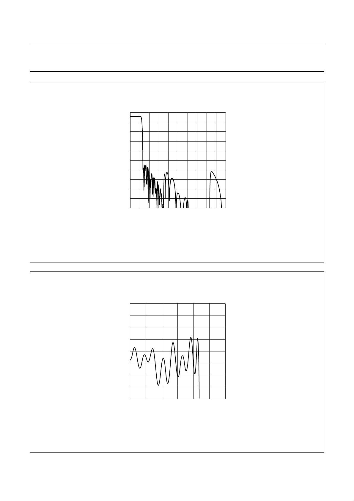
The digital filter interpolates from 1 to 128fs by cascading
a half-band filter and a FIR filter, see Table 2. The overall
filter characteristic ofthe digital filters is illustrated in Fig.3,
andthe pass-band ripple isillustratedin Fig.4. Both figures
are with a 44.1 kHz sampling frequency.
Table 2 Interpolation filter characteristics
ITEM CONDITION VALUE (dB)
Pass-band ripple 0 to 0.45f
Stop band >0.55f
Dynamic range 0 to 0.45f
s
s
s
±0.02
−55
>114
DC gain −−3.5
1999 Oct 12 7
The output voltage of the FSDAC scales proportionally
with the power supply voltage.
8.7 Static mode
The UDA1328 is set to static mode by setting the STATIC
pin HIGH. The function of 6 pins of the device now get
another function as can be seen in Table 1.
8.7.1 SYSTEM CLOCK SETTING
In static mode pin 18 (L3CLOCK) is used to select the
system clock setting.When pin 18 is LOW, the device isin
256fs mode, when pin 18 is HIGH the device is in 384f
s
mode.
Philips Semiconductors Preliminary specification
Multi-channel filter DAC UDA1328T
8.7.2 DE-EMPHASIS CONTROL
Instaticpin mode the pinsDEEM0 and DEEM1controlthe
de-emphasis mode; see Table 3.
Table 3 De-emphasis control
DEEM MODE DEEM1 DEEM0
No de-emphasis 0 0
32 kHz de-emphasis 0 1
44.1 kHz de-emphasis 1 0
48 kHz de-emphasis 1 1
8.7.3 DIGITAL INTERFACE FORMATS
Instaticpin mode the digitalaudiointerfaceformats can be
selected via pin 17 (SF1) and 19 (SF0). The following
interface formats can be selected (see also Table 4):
• I2S-bus with data word length of up to 24 bits
• LSB-justified format with data word length of
16, 20 or 24 bits.
Table 4 Input format selection in the static mode
INPUT FORMAT SF1 SF0
2
I
S-bus 0 0
LSB-justified 16 bits 0 1
LSB-justified 20 bits 1 0
LSB-justified 24 bits 1 1
8.8 L3 mode
The device is set to L3 mode by setting the STATIC pin to
LOW. The device can then be controlled via the L3
microcontroller interface (see Chapter 9).
8.8.1 DIGITAL INTERFACE FORMATS
The following interface formats can be selected in the
L3 mode:
• I2S-bus with data word length of up to 24 bits
• MSB-justified with data word length of up to 24 bits
• LSB-justified format with data word length of 16, 18,
20 or 24 bits.
8.8.2 L3 ADDRESS
TheUDA1328canbe addressed via the L3 microcontroller
interface using oneof two addresses.This is done in order
to individually control the UDA1328 and other Philips
DACs or CODECs via the same L3 bus.
The address can be selected using pin 25 (DEEM0) in
L3 mode.When pin 25 isset LOW, theaddress is 000100.
When pin 25 is set HIGH the address is 000101.
It should be noted that thedigital audio interfaceholds that
the BCK frequency can be 64 times the WS maximum
frequency, or f
BCK
≤ 64 × f
WS
1999 Oct 12 8
Philips Semiconductors Preliminary specification
Multi-channel filter DAC UDA1328T
fs= 6.14400 MHz
handbook, halfpage
0
volume
(dB)
−20
−40
−60
−80
−100
0 200
Fig.3 Overall frequency characteristics.
MGR981
40 80 120 160
f (kHz)
−3.45
handbook, halfpage
V
o
(dB)
−3.47
−3.49
−3.51
−3.53
0 102030
fs= 6.14400 MHz
Fig.4 Pass-band ripple of all filters.
1999 Oct 12 9
MGR982
f (kHz)
 Loading...