

Philips UDA1320ATS Datasheet

INTEGRATED CIRCUITS
DATA SH EET
UDA1320ATS
Low-cost stereo filter DAC
Preliminary specification
File under Integrated Circuits, IC01
1999 Oct 11

Philips Semiconductors Preliminary specification
Low-cost stereo filter DAC UDA1320ATS
CONTENTS
1 FEATURES
1.1 General
1.2 Multiple format input interface
1.3 DAC digital sound processing
1.4 Advanced audio configuration
2 APPLICATIONS
3 GENERAL DESCRIPTION
4 ORDERING INFORMATION
5 QUICK REFERENCE DATA
6 BLOCK DIAGRAM
7 PINNING
8 FUNCTIONAL DESCRIPTION
8.1 System clock
8.2 Application modes
8.3 Multiple format input interface
8.4 Static pin mode
8.5 Pin compatibility
8.6 Interpolation filter (DAC)
8.7 Noise shaper
8.8 Filter-Stream DAC
9 L3 INTERFACE DESCRIPTION
9.1 The L3 interface
9.2 Data transfer mode
9.3 Programming the features
10 LIMITING VALUES
11 HANDLING
12 QUALITY SPECIFICATION
13 THERMAL CHARACTERISTICS
14 DC CHARACTERISTICS
15 AC CHARACTERISTICS
15.1 Analog
15.2 Digital
16 APPLICATION INFORMATION
17 PACKAGE OUTLINE
18 SOLDERING
18.1 Introduction
18.2 Reflow soldering
18.3 Wave soldering
18.4 Repairing soldered joints
19 DEFINITIONS
20 LIFE SUPPORT APPLICATIONS
1999 Oct 11 2

Philips Semiconductors Preliminary specification
Low-cost stereo filter DAC UDA1320ATS
1 FEATURES
1.1 General
• Low power consumption.
• 2.7 to 3.6 V power supply.
• Selectable controlvia L3 microcontroller interface or via
static pin control.
• 256, 384 and 512fs system clock (f
the L3 interface or 256 and 384fs clock mode via static
pin control
• supports sampling frequencies from 16kHz to 48kHz.
• Integrated digital filter plus non inverting DAC
Digital-to-Analog Converter (DAC).
• Easyapplication and no analog postfilteringrequiredfor
DAC.
• Slave mode only applications.
• Small package size (SSOP16).
1.2 Multiple format input interface
• I2S-bus, MSB-justified and LSB-justified 16,18 and 20
bits format compatible (in L3-mode).
• I2S-bus and LSB-justified 16,18 and 20 bits format
compatible in static mode.
• 1fs input format data rate.
1.3 DAC digital sound processing
• Digital logarithmic volume control via L3.
• Digital de-emphasis for 32, 44.1 and 48 kHz fs via
L3 or 44.1 kHz fs via static pin control.
• Soft mute via static pin control or via L3 interface.
1.4 Advanced audio configuration
• Stereo line output (under L3 volume control)
• High linearity, wide dynamic range, low distortion.
), selectable via
sys
2 APPLICATIONS
• Portable digital audio equipment, see Fig.8.
• Set-top boxes
3 GENERAL DESCRIPTION
TheUDA1320ATS/N2 is asingle-chip non inverting stereo
DAC employing bitstreamconversion techniques. The low
power consumption and low voltage requirements make
the device eminently suitable for use in digital audio
equipment which incorporates playback functions.
The UDA1320ATS/N2 supports the I2S-bus data format
with word lengths of up to 20 bits, the MSB-justified data
format with word lengths of up to 20 bits and the
LSB-justified serial data format with word lengths of 16,
18 and 20 bits.
The UDA1320ATS/N2 can be used in two modes, either
L3-mode or static pin mode.
In the L3-mode, all digital soundprocessing features must
becontrolled via the L3 interface, includingtheselectionof
the system clock setting.
In the two static-modes, the UDA1320ATS/N2 can be
operated in the 256fs and 384fs system clock mode. The
mute,de-emphasisfor 44.1 kHz and 4 digital inputformats
(I2S and 16, 18, 20 bits LSB formats) can be selected via
static pins. The L3 interface cannot be used in this
application mode, also, volume control is not available in
this mode.
4 ORDERING INFORMATION
TYPE NUMBER
NAME DESCRIPTION VERSION
UDA1320ATS SSOP16 plastic shrink small outline package; 16 leads; body width 4.4 mm SOT369-1
1999 Oct 11 3
PACKAGE

Philips Semiconductors Preliminary specification
Low-cost stereo filter DAC UDA1320ATS
5 QUICK REFERENCE DATA
SYMBOL PARAMETER CONDITIONS MIN. TYP. MAX. UNIT
Supply
V
DDA
V
DDD
I
DDA
I
DDD
T
amb
DAC
V
o(rms)
(THD + N)/S total harmonic distortion plus
S/N signal-to-noise ratio code = 0; A-weighted − 100 95 dB
α
cs
T
amb
analog supply voltage 2.7 3.3 3.6 V
digital supply voltage 2.7 3.3 3.6 V
DAC supply current − 6.5 − mA
digital supply current − 3.0 − mA
operating ambient temperature −20 − +85
°
C
output voltage (RMS value) note 1, 2 − 1.0 − V
at 0 dB −−90 −85 dB
noise-to-signal ratio
at −60 dB; A-weighted −−38 −35 dB
channel separation − 100 − dB
operating ambient temperature −30 − +85
°
C
Notes
1. the output voltage has been changed with respect to the UDA1320TZ/N1.
2. the output voltage scales linearly with the power supply voltage.
6 BLOCK DIAGRAM
handbook, full pagewidth
BCK
WS
DATAI
SYSCLK
V
O(L)
1
2
3
UDA1320A
6
14
V
DDD
4
DIGITAL INTERFACE
VOLUME/MUTE/DE-EMPHASIS
INTERPOLATION FILTER
NOISE SHAPER
DAC
V
DAC
SSD
5
INTERFACE
CONTROL
7
APPSEL
11
APPL0
10
APPL1
9
APPL2
8
APPL3
16
V
O(R)
13 12
V
DDA
V
SSA
Fig.1 Block diagram.
1999 Oct 11 4
15
V
REF(DAC)
MGM816
Philips Semiconductors Preliminary specification
Low-cost stereo filter DAC UDA1320ATS
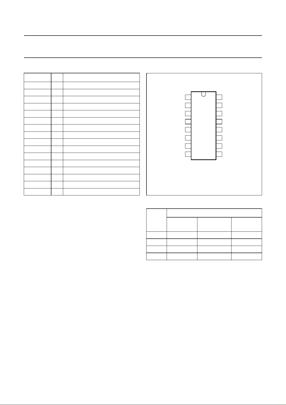
7 PINNING
SYMBOL PIN
DESCRIPTION
BCK 1 bit clock
WS 2 word select
DATAI 3 data input
V
DDD
V
SSD
SYSCLK 6 system clock: 256f
4 digital power supply
5 digital ground
, 384fs, 512f
s
s
APPSEL 7 application mode select
APPL3 8 application pin 3
APPL2 9 application pin 2
APPL1 10 application pin 1
APPL0 11 application pin 0
V
REF(DAC)
V
DDA
V
O(L)
V
SSA
V
O(R)
12 DAC reference voltage
13 analog supply voltage
14 left output voltage
15 analog ground
16 right output voltage
8 FUNCTIONAL DESCRIPTION
8.1 System clock
The UDA1320ATS/N2 operates in slave mode only. This
means in all applications the system devices must provide
the system clock. The system frequency is selectable and
depends on the mode of operation.
The options are 256fs, 384fs and 512fs for the L3 mode
and 256fsplus 384fsfor the static mode. The system clock
must be locked in frequency to the digital interface input
signals.
The UDA1320ATS/N2 supports sampling frequencies
from 16kHz up to 48kHz
8.2 Application modes
The application mode can be set with the tri-value
APPSEL pin, to L3 mode (APPSEL = V
two static modes (APPSEL = 0.5V
APPSEL = V
). See Table 1 for APPL0 to APPL3 pin
DDD
DDD
) or to either of
SSD
or
functions (active = HIGH).
handbook, halfpage
BCK
WS
DATAI
V
DDD
V
SSD
1
2
3
4
UDA1320A
5
6
7
8
MGM817
16
15
14
13
12
11
10
9
V
O(R)
V
SSA
V
O(L)
V
DDA
V
REF(DAC)
APPL0SYSCLK
APPL1APPSEL
APPL2APPL3
Fig.2 Pin configuration.
Table 1 Selection modes via APPSEL (note 1)
APPSEL
PIN
V
SSD
0.5V
(384fs)
DDD
V
DDD
(256fs)
APPL0 TEST MUTE MUTE
APPL1 L3CLOCK DEEM DEEM
APPL2 L3MODE SF0 SF0
APPL3 L3DATA SF1 SF1
For example, in static pin control mode, the output signal
can be soft muted by setting APPL0 HIGH. De-emphasis
can be switched on for 44.1 kHz by setting APPL1 HIGH.
APPL1 LOW will disable de-emphasis.
Note that when L3 interface is used, an L3 initialisation
must be done when the IC is powered up!
In L3 mode pin APPL0 must be set to LOW.
1999 Oct 11 5

Philips Semiconductors Preliminary specification
Low-cost stereo filter DAC UDA1320ATS
8.3 Multiple format input interface
L3 mode:
• I2S-bus with data word length of up to 20 bits
• MSB-justified format with data word length up to 20 bits
• LSB-justified format with data word length of 16,
IMPORTANT: UDA1320ATS/N2 differs from the
UDA1320TZ/N1 with respect to:
• in the static mode 384fs is supported instead of 512fs.
• the output voltage of the DAC. In the UDA1320TZ/N1
this is 800mVrmsat 3.0V, now it is 1Vrms at3.3V power
supply
18 or 20 bits.
8.6 Interpolation filter (DAC)
8.4 Static pin mode
The digital filter interpolates from 1 to 128fs by cascading
The UDA1320ATS/N2 supports the following data input
a recursive filter and a FIR filter, see Table 3.
name formats in the static pin mode (via SF0 and SF1):
• I2S bus with data word length of up to 20 bits
• LSB-justified format with data word length of 16,
18 or 20 bits.
See Table 2, for the static pin codes of the 4 formats,
selectable via SF0 and SF1.
Table 3 Interpolation filter characteristics
ITEM CONDITION VALUE (dB)
Pass-band ripple 0 to 0.45f
Stop band >0.55f
Dynamic range 0 to 0.45f
The UDA1320ATS/N2 also accepts double speed data for
double speed data monitoring purposes.
Table 2 Input format selection using SF0 and SF1
FORMAT SF0 SF1
2
I
S00
LSB-justified 16 bits 0 1
8.7 Noise shaper
The 3rd-order noise shaper operates at 128f
in-band quantization noise to frequencies well above the
audio band. This noise shaping technique enables high
signal-to-noise ratios to be achieved. The noise shaper
output is converted into an analog signal using a
Filter-Stream DAC (FSDAC).
LSB-justified 18 bits 1 0
LSB-justified 20 bits 1 1
8.8 Filter-Stream DAC
s
s
s
±0.1
−50
108
. It shifts
s
The formats are illustrated in Fig.3. Left and right
data-channel words are time multiplexed. The WS signal
must have 50% duty-factor for all LSB-justified modes.
For BCK and WS holds that the BCK frequency must be
equal or smaller then 64 times WS, or f
=< 64*fWS in
BCK
both L3 and static mode.
8.5 Pin compatibility
InL3 interface mode theUDA1320ATS/N2canbe used on
boards that are designed for the UDA1322. The software
for UDA1322 can be used for the UDA1320ATS/N2 to
control de-emphasis, volume control and mute and also
the status settings like system clock setting andinput data
format.
1999 Oct 11 6
The FSDAC is a semi-digital reconstruction filter that
converts the 1-bit data stream of the noise shaper to be
analog output voltage. The filter coefficients are
implemented as current sources and are summed at
virtual ground of the output operational amplifier. In this
way very high signal-to-noise performance and low clock
jitter sensitivity is achieved. A post-filter isnot needed due
to the inherent filter function of the DAC. On-board
amplifiers convert the FSDAC output current to an output
voltage signal capable of driving a line output.
The output voltage of the FSDAC scales linearly with the
power supply voltage.
 Loading...