

Philips UDA1309H Datasheet

INTEGRATED CIRCUITS
DATA SH EET
UDA1309H
Low-power stereo bitstream
ADC/DAC
Product specification
Supersedes data of 1996 Jul 18
File under Integrated Circuits, IC01
1998 Jan 06

Philips Semiconductors Product specification
Low-power stereo bitstream ADC/DAC UDA1309H
FEATURES
• Low power
• Integrated high-pass filter to cancel DC offset (ADC)
• Analog loop-through function
• Multiple digital input/output formats possible
• 256fs system clock frequency
• Several power-down modes
• Digital de-emphasis (DAC)
• Overload detector to enable automatic recording level
adjustment (ADC)
• High dynamic range
• DAC requires only one capacitor for post-filtering
• Small 44-pin quad flat pack with 0.8 mm pitch
• 256fs system clock frequency in Analog-to-Digital (AD)
and Digital-to-Analog (DA) mode
• Choice of three system clock frequencies
(192fs, 256fs or 384fs) in DA mode.
APPLICATION
• Portable digital audio equipment.
GENERAL DESCRIPTION
The UDA1309H is a single chip stereo analog-to-digital
and digital-to-analog converter employing bitstream
conversion techniques. The device is eminently suitable
for use in low-power portable digital audio equipment
which incorporates recording and playback functions.
ORDERING INFORMATION
TYPE
NUMBER
UDA1309H QFP44 plastic quad flat package; 44 leads (lead length 1.3mm); body 10× 10 × 1.75 mm SOT307-2
NAME DESCRIPTION VERSION
PACKAGE
1998 Jan 06 2

Philips Semiconductors Product specification
Low-power stereo bitstream ADC/DAC UDA1309H
QUICK REFERENCE DATA
V
DDD=VDDA=VDDO=VDDD(F)
mode 1; fi= 1 kHz; 16-bit input data; conversion rate = 44.1 kHz; measurement bandwidth = 10 Hz to 20 kHz; unless
otherwise specified.
SYMBOL PARAMETER CONDITIONS MIN. TYP. MAX. UNIT
Supply
V
DDA(AD)
V
DDA(DA)
V
DDO
ADC analog supply voltage (pin 8) 4.5 5.0 5.5 V
DAC analog supply voltage (pin 25) 4.5 5.0 5.5 V
operational amplifiers supply voltage
(pin 19)
V
DDD
ADC and DAC digital supply voltage
(pin 28)
V
DDD(F)
I
DDA(AD)
I
DDA(DA)
I
DDO
digital filters supply voltage (pin 34) 4.5 5.0 5.5 V
ADC analog supply current (pin 8) − 9 13.5 mA
DAC analog supply current (pin 25) − 4.5 6.8 mA
operational amplifiers supply current
(pin 19)
I
DDD
ADC and DAC digital supply current
(pin 28)
I
DDD(F)
T
amb
digital filters supply current (pin 34) − 24 36 mA
operating ambient temperature −20 − +75 °C
Analog-to-digital converter
V
I(rms)
input voltage (RMS value) note 1 0.9 1.0 1.1 V
(THD + N)/S total harmonic distortion plus
noise-to-signal ratio
S/N idle channel signal-to-noise ratio V
α
cs
channel separation − 90 − dB
Digital-to-analog converter
V
O(rms)
output voltage (RMS value) note 2 0.9 1.0 1.1 V
(THD + N)/S total harmonic distortion plus
noise-to-signal ratio
S/N idle channel signal-to-noise ratio code 0000H; A-weighted − 104 − dB
α
cs
channel separation 90 100 − dB
=5V; V
SSD=VSSA=VSSO=VSSD(F)
at 0 dB −−85 tbf dB
at −60 dB; A-weighted −−35 −30 dB
= 0 V; A-weighted tbf 95 − dB
I
at 0 dB −−90 −82 dB
at −60 dB; A-weighted −−38 −34 dB
at −60 dB; A-weighted; note 3 −−44 − dB
=0V; T
=25°C; full scale sine wave input;
amb
4.5 5.0 5.5 V
4.5 5.0 5.5 V
− 14 21 mA
− 0.2 0.5 mA
Notes
1. VI for full scale digital output is a function of V
[1.0 V (RMS) at V
DDA(AD)
digital domain].
2. At full scale digital input; no de-emphasis; V
is a function of V
O(rms)
3. 18-bit input data.
1998 Jan 06 3
DDA(AD)
DDA(DA)
= 5.0 V is equivalent to −1.0 dB in the
.

Philips Semiconductors Product specification
Low-power stereo bitstream ADC/DAC UDA1309H
BLOCK DIAGRAM
10
µF
µF
ok, full pagewidth
OL
V
analog output
SSA(DA)
V
DDA(DA)
V
SSD(F)
V
DADEM
MODE2
CLKEDGE
TEST0
1 nF
SSO
V
DDO
V
DDD(F)
V
MODE0
MODE1
TEST1
SYSCLK
OLDACL
21
V
22
20
19
26
25
33
34
30
3
42
43
44373840
ref(neg)
V
9
0.22
ref
DA
1.6 kΩ
OR
V
24
DACR
23
SSD
V
27
DDD
V
28
SS(I/O)
V
39
35 29
31
32
36
6
41
1
42
5
1 nF
DAPON
DASDA
ADWS
ADENB
18
1.6 kΩ
DAC
MODE SELECT
Vm
FILTER
DIGITAL
DIGITAL
INTERFACE
DIGITAL
INTERFACE
DAC
UDA1309H
OR
V
analog output
DABCK
DAWS
ANLPTR
ADPON
ADSDA
ADBCK
OVLOAD
MBH527
Fig.1 Block diagram.
DDA(AD)
V
47 µF
IL
V
analog input
4.7 kΩ
0.22 µF
330 pF
7
SSA(AD)
V
ADC
8
DDA(AD)
V
ref(pos)
1112
V
BAOL
4.7 kΩ
BAIL
13
ref
V
10
0.22 µF
DIGITAL
DAC
I
CURRENT
REFERENCE
17
ref
I
47
FILTER
kΩ
1998 Jan 06 4
ADC
Vm
BAOR
15
4.7 kΩ
330 pF
14
BAIR
16
ref
AD
0.22 µF
47 µF
4.7 kΩ
IR
V
analog input
Supply decoupling on pins 19, 25, 28 and 34; 0.22 µF (ceramic), 47 µF (electrolytic).
Capacitance at pin 11 should be close to pins 11 and 9.
Philips Semiconductors Product specification
Low-power stereo bitstream ADC/DAC UDA1309H
PINNING
SYMBOL PIN DESCRIPTION
ADBCK 1 ADC input bit clock; 32f
ADWS 2 ADC word select input at f
MODE0 3 ADC/DAC mode select input
ADENB 4 ADC serial data enable input (active HIGH)
OVLOAD 5 ADC output overload flag (active LOW)
ADPON 6 ADC power-on-mode input (active HIGH)
V
SSA(AD)
V
DDA(AD)
V
ref(neg)
V
ref
V
ref(pos)
7 ADC analog ground supply voltage
8 ADC analog supply voltage
9 ADC negative reference voltage input (ground)
10 ADC decoupling capacitor
11 ADC positive reference voltage decoupling capacitor
BAOL 12 ADC input amplifier output left
BAIL 13 ADC input amplifier virtual ground left
BAIR 14 ADC input amplifier virtual ground right
BAOR 15 ADC input amplifier output right
AD
I
ref
DA
V
V
V
ref
ref
DDO
SSO
OL
16 ADC decoupling capacitor
17 ADC/DAC reference current resistor input
18 DAC decoupling capacitor
19 ADC/DAC operational amplifier supply voltage
20 ADC/DAC operational amplifier ground supply voltage
21 DAC output voltage left
DACL 22 DAC output current left
DACR 23 DAC output current right
V
OR
V
DDA(DA)
V
SSA(DA)
V
SSD
V
DDD
24 DAC output voltage right
25 DAC analog supply voltage
26 DAC analog ground supply voltage
27 ADC/DAC digital ground supply voltage
28 ADC/DAC digital supply voltage
DAPON 29 DAC power-on-mode input (active HIGH)
DADEM 30 DAC digital de-emphasis input (active HIGH)
DABCK 31 DAC input bit clock; 32f
DAWS 32 DAC word select input at f
V
SSD(F)
V
DDD(F)
33 ADC/DAC digital filters ground supply voltage
34 ADC/DAC digital filters supply voltage
DASDA 35 DAC serial data input
ANLPTR 36 ADC/DAC analog loop-through input (active HIGH)
TEST0 37 ADC/DAC enable test mode 0 input (LOW is normal mode)
TEST1 38 ADC/DAC enable test mode 1 input (LOW is normal mode)
V
SS(I/O)
39 ADC/DAC digital input/output ground supply voltage
SYSCLK 40 ADC/DAC system clock input (f
or 64f
s
s
s
, 48fs or 64f
s
s
sys
s
= 256fs; DAC also 192fs and 384fs)
1998 Jan 06 5

Philips Semiconductors Product specification
Low-power stereo bitstream ADC/DAC UDA1309H
SYMBOL PIN DESCRIPTION
ADSDA 41 ADC serial data output
MODE1 42 ADC/DAC mode 1 select input
MODE2 43 ADC/DAC mode 2 select input
CLKEDGE 44 ADC/DAC input bit clock rising/falling edge
handbook, full pagewidth
ADBCK
ADWS
MODE0
ADENB
OVLOAD
ADPON
V
SSA(AD)
V
DDA(AD)
V
ref(neg)
V
ref(pos)
SSO
DDD(F)
V
DASDA
35
34
21
22
OL
V
DACL
33
32
31
30
29
28
27
26
25
24
23
V
DAWS
DABCK
DADEM
DAPON
V
V
V
V
V
DACR
MBH526
SSD(F)
DDD
SSD
SSA(DA)
DDA(DA)
OR
MODE1
MODE2
43
42
13
14
BAIL
BAIR
ADSDA
41
15
BAOR
CLKEDGE
44
1
2
3
4
5
6
7
8
9
V
10
ref
11
12
BAOL
SS(I/O)
SYSCLK
V
40
39
UDA1309H
16
17
ref
ref
I
AD
TEST1
38
18
ref
DA
TEST0
37
19
DDO
V
ANLPTR
36
20
V
Fig.2 Pin configuration.
1998 Jan 06 6
Philips Semiconductors Product specification
Low-power stereo bitstream ADC/DAC UDA1309H
FUNCTIONAL DESCRIPTION
Figure 1 illustrates the various components of the
UDA1309H.
The analog-to-digital converter is a bitstream type
converter, both channels are sampled simultaneously.
The digital-to-analog converter is a BCC (Bitstream
Continuous Calibration) type converter. The digital filter for
the ADC is a bit serial IIR filter that produces a fairly linear
phase response up to 15 kHz. A high-pass filter is
incorporated in the down-sampling path to remove DC
offsets. An overload detection circuit is incorporated to
facilitate automatic recording level adjustment.
The digital up-sample filter for the DAC is partly IIR, with
virtual linear phase response up to 15 kHz, and partly FIR.
A switchable digital de-emphasis circuit is also
incorporated. Due to the BCC principle used, the DAC
needs only single pole post-filtering (one external
capacitor) to meet the out-of-band suppression
requirement.
The ADC and DAC channels have separate power-down
modes, to reduce power if one of them is not in use.
An analog loop-through function enables analog-input
analog-output mode without using the ADC and DAC
converters or filters, thereby switching them off to reduce
power consumption.
The digital interfaces accommodates, 16 and 18-bit,
2
I
S-bus and LSB justified formats. The ADC digital output
can be made 3-state by means of the ADENB signal, this
enables the use of a digital bus.
The UDA1309H interface accommodates slave mode
only, therefore, the system ICs must provide the system
clock, bit clock and word clock signals. For the DAC, the
UDA1309H accepts the data together with these clocks,
for the ADC it delivers the data in response to these clocks.
Within one stereo frame, the first sample always
represents the left channel. When sending data the
unused bit positions are set to zero, when receiving data
these bit positions are don't cares.
To accommodate the various interface formats and
system clock frequencies four control pins are provided,
MODE0 to MODE2 for mode selection and CLKEDGE
which selects the active edge of the BCK signal. Table 1
gives the interface mode selection, Fig.3 illustrates the
ADC/DAC data formats and Fig.5 the operating modes.
The section of the UDA1309H is designed to
accommodate two main modes:
1. The 256fs mode in which analog-to-digital and
digital-to-analog can be used.
2. The 192fs or 384fs mode (digital-to-analog only).
Table 1 Interface mode selection
DEVICE PIN ADC/DAC FORMATS
MODE 2 MODE 1 MODE 0 TYPE BITS BCK SYS; f
0 0 0 LSB justified 16 32f
0 0 1 LSB justified 16 64f
0 1 0 LSB justified 16 48f
0 1 1 LSB justified 18 64f
100I
101I
110I
111I
2
S-bus 16 32f
2
S-bus 16 64f
2
S-bus 16 48f
2
S-bus 18 64f
s
s
s
s
s
s
s
s
Note
1. Only digital-to-analog.
Table 2 Clock edge mode
VALID EDGE OF BCK
CLKEDGE
ADC DAC
0 falling rising
1 rising falling
256f
256f
192f
256f
256f
256f
384f
256f
sys
s
s
(1)
s
s
s
s
(1)
s
s
FIGURE
3(a)
3(b)
4(a)
3(c)
3(d)
3(e)
4(b)
3(f)
1998 Jan 06 7
Philips Semiconductors Product specification
Low-power stereo bitstream ADC/DAC UDA1309H
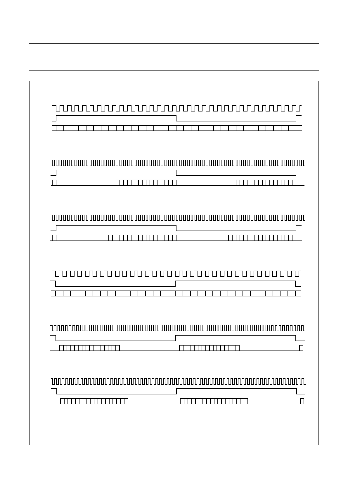
handbook, full pagewidth
BCK
WS
SDA
LSB MSB
BCK
WS
SDA
LSB
BCK
WS
SDA
LSB
MSB
LEFT
LEFT
MSB
LEFT
LSB JUSTIFIED 32fs 16-BIT
LSB MSB
(a)
LSB JUSTIFIED 64fs 16-BIT
LSB
(b)
LSB JUSTIFIED 64fs 18-BIT
LSB
(c)
2
I
S 32fs 16-BIT
RIGHT
RIGHT
MSB LSB
RIGHT
MSB
LSB
LSB
MSB
BCK
WS
SDA
BCK
WS
SDA
BCK
WS
SDA
LEFT
LSB MSB
LEFT
MSB
MSB LSB
LSB
LEFT
Fig.3 DAC and ADC data formats (continued in Fig.4).
RIGHT
LSB MSB
(d)
2
S 64fs 16-BIT
I
RIGHT
MSB LSB MSB
(e)
2
S 64fs 18-BIT
I
RIGHT
MSB
(f)
LSB MSB
LSB
MGE767
1998 Jan 06 8
 Loading...