

Philips UCB1510DB Datasheet

1. Description
2. Features
UCB1510
AC97 digital modem codec
Rev. 01 — 4 February 2000 Preliminary specification
The UCB1510 is a single chip, integrated mixed signal telecom codec that can
directly be connected to a DAA and supports high speed modem protocols. The
general purpose I/O pins provide programmable inputs and/or outputs to the system.
The UCB1510 has a serial AClink interface intended to communicate to the system
controller. Both the codec input data and codec output data and the control register
data are multiplexed on this interface.
c
c
3. Applications
■ Sigma delta telecom codec with programmable sample rate, including digitally
controlled input voltage level, mute, loop back and clip detection functions. The
telecom codec can be directly connected to a Data Access Arrangement (DAA)
and includes a built in sidetone suppression circuit
■ AClink (rev 2.1) interface with secondary codec support
■ 3.3 V supply voltageand built in power saving modes make the UCB1510 optimal
for portable and battery powered applications
■ 5 V tolerant interface for motherboard/PC add on
■ Maximum operating current 25 mA
■ 8 general purpose IO pins for line interface control
■ Interrupt detection driven wake up sequence for ring detect
■ Low cost 12.288 MHz crystal
■ Standalone modems
■ Integrated modems
■ Audio/Modem Riser (AMR) Cards
■ Mobile Daughter Cards (MDC)
Philips Semiconductors
UCB1510
AC97 digital modem codec
4. Ordering information
Table 1: Ordering information
Type number Package
Name Description Version
UCB1510DB SSOP28 plastic shrink small outline package, 28 leads, body width 5.3mm SOT341-1
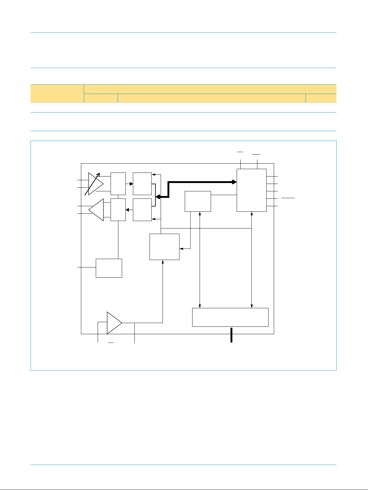
5. Block diagram
A0
PON
TINP
TINN
TOUTP
TOUTN
VREFBYP
Voltage
reference
XTAL_IN/A1
ADC
DAC
down
sample
filter
up
sample
filter
XTAL_OUT
Clock buffers &
sample rate
dividers
Line1 PCM flow
data /
control
registers
GPIO
IO[7:0]
Serial bus
interface
SDOUT
SDIN
SYNC
RESET
BIT_CLK
Fig 1. Block diagram
9397 750 06856
Preliminary specification Rev. 01 — 4 February 2000 2 of 32
© Philips Electronics N.V. 2000. All rights reserved.

Philips Semiconductors
6. Pinning information
6.1 Pinning
UCB1510
AC97 digital modem codec
VDDD
IO0
IO1
IO2
IO3
RESET
PON
SYNC
SDOUT
VSSD
SDIN
BIT_CLK
VDDD
Fig 2. Pin configuration
6.2 Pin description
1
2
3
4
5
6
7
A0
8
9
10
11
12
13
14 15
UCB1510
28
XTAL_OUT
27
XTAL_IN/A1
26
VSSA
25
TINN
24
TINP
23
VREFBYP
22
TOUTN
21
TOUTP
20
VDDA
19
VSSD
18
IO7
17
IO6
16
IO5
IO4
Table 2: Pin description
Symbol Pin Reset
state
V
DDD
1 - S digital supply
[1]
Type
IO0 2 input I/O
IO1 3 input I/O
IO2 4 input I/O
IO3 5 input I/O
RESET 6 - I
A0 7 - I
PON 8 - I
SYNC 9 - I/O
SDOUT 10 - I
V
SSD
SDIN 12 0
BIT_CLK 13 V
DDD
11 - S digital ground
[4]
[3]
O
I/O
14 - S digital supply
IO4 15 input I/O
[2]
Description
C
C
C
C
C
C
general purpose I/O pins
general purpose I/O pins
general purpose I/O pins
general purpose I/O pins
asynchronous reset input
address select (for secondary codec) -
inverted polarity
C
C
C
C
C
C
asynchronous cold reset
AClink synchronization input
AClink data input
AClink data output
AClink serial interface clock
general purpose I/O pins
9397 750 06856
Preliminary specification Rev. 01 — 4 February 2000 3 of 32
© Philips Electronics N.V. 2000. All rights reserved.

Philips Semiconductors
UCB1510
AC97 digital modem codec
Table 2: Pin description
Symbol Pin Reset
IO5 16 input I/O
IO6 17 input I/O
IO7 18 input I/O
V
SSD
V
DDA
19 - S digital ground
20 - S analog supply
TOUTP 21 hi Z O
TOUTN 22 hi Z O
VREFBYP 23 hi Z I/O
TINP 24 - I
TINN 25 - I
V
SSA
XTAL_IN/
26 - S analog ground
A1 27 -
…continued
[1]
state
[3]
Type
C
C
C
A
A
A
A
A
IA/I
C
[2]
Description
general purpose I/O pins
general purpose I/O pins
general purpose I/O pins
positive telecom codec output
negative telecom codec output
external reference voltage bypass
positive telecom codec input
negative telecom codec input
Xtal oscillator/master clock input or inverted
secondary address
XTAL_OUT 28 -
[1] After cold or warm reset, the AClink interface is active with MLNK bit reset.
[2] I/OC = CMOS bidirectional; ID = digital input; S = supply; OA = analog output; IC = CMOS input;
IA= analog input; I/OA = analog bidirectional; OC = CMOS output.
[3] BIT_CLK is an input for AClink secondary codec, an output for primary codec. When BIT_CLK is an
output, the XTAL oscillator is active.
[4] SDIN is driving a 0 until a valid SYNC framing signal is received after cold reset.
[3]
O
A
Xtal oscillator output
9397 750 06856
Preliminary specification Rev. 01 — 4 February 2000 4 of 32
© Philips Electronics N.V. 2000. All rights reserved.
Philips Semiconductors
7. Functional description
The functional description of the devices id described in Section 8 through
Section 15.
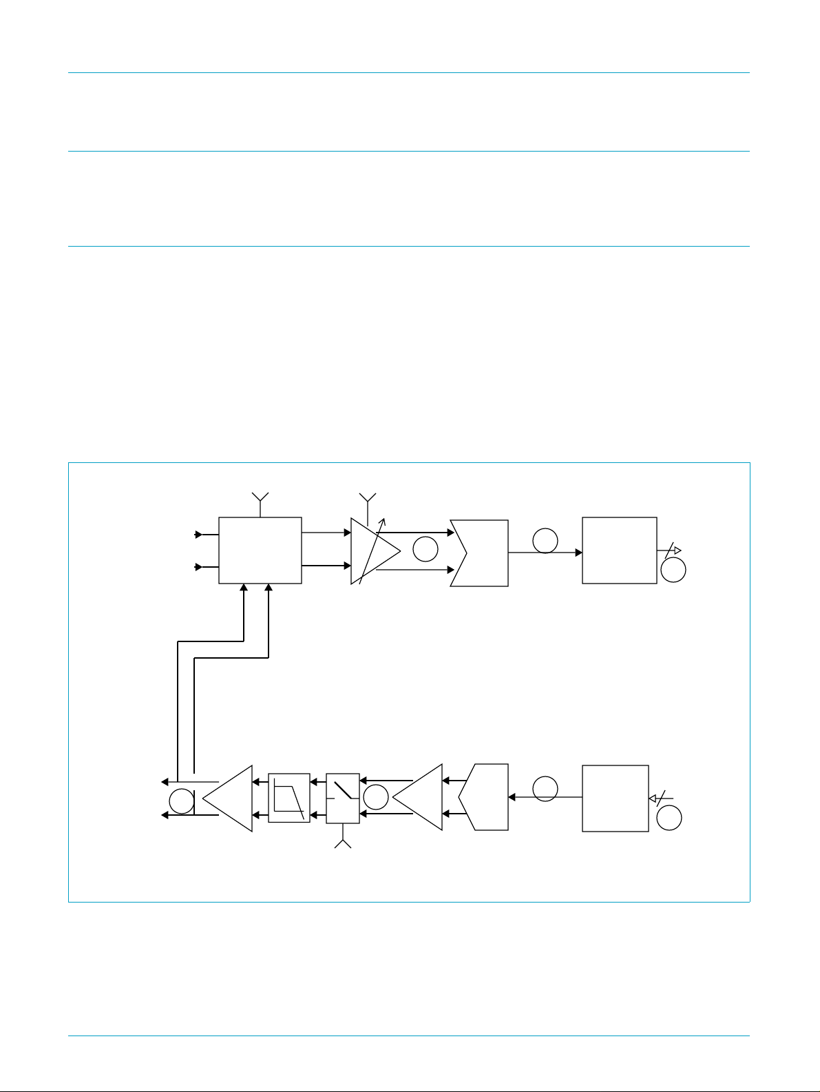
8. Telecom codec
The telecom codec contains an input channel, built up from a 64 times oversampling
sigma delta analog to digital converter (ADC) with digital decimation filters,
programmable gain and attenuation and built-in sidetone suppression circuit.
The output path consists of a digital up sample filter, a 64 time oversampling 4 bit
digital to analog converter (DAC) circuit with integrated filter followed by a differential
output driver, capable of directly driving a 600 Ω isolation transformer. The output
path includes a mute function. The telecom codec also incorporates loop back
modes, in which codec output path and the input path are connected in series. The
loop back tap and entry points are identified as circled letters in Figure 3, loop back
modes are described in the AClink register definition.
UCB1510
AC97 digital modem codec
TOUTP
TOUTN
TINP
TINN
E
sidetone_enable
SIDETONE
SUPPRESSION
CIRCUIT
ADC[3:2]
DAC Mute
ADC
J
D
DAC
H
C
DIGITAL
DECIMATION
FILTER
DIGITAL
NOISE
SHAPER
14
G
14
B
Fig 3. Telecom codec block diagram
The telecom sample rate (fst) is derived from the AC master clock and is
programmable using the sample rate registers. Not all AC97 specified sample rates
are supported, refer to Table 3 “Sampling frequencies” for details.
PCM data is transferred in the slot 5 of the AClink.
9397 750 06856
Preliminary specification Rev. 01 — 4 February 2000 5 of 32
© Philips Electronics N.V. 2000. All rights reserved.

Philips Semiconductors
Table 3: Sampling frequencies
Sampling frequency (Hz) Register 0x40
7200 0x1C20 no recommended
8000 0x1F40 yes required
8228.57 (57600/7) 0x2024 no recommended
8400 0x20D0 no recommended
9000 0x2328 no recommended
9600 0x2580 yes required
10285.71 (72000/7) 0x282D no recommended
12000 0x2EE0 yes recommended
13714.29 (96000/7) 0x3592 yes required
16000 0x3E80 yes required
19200 0x4B00 yes recommended
24000 0x5DC0 yes recommended
48000 0xBB80 no recommended
value
UCB1510
AC97 digital modem codec
Support AC ‘97
requirements
Any programmed vlaue above 24 kHz will lead to a 24 kHz sampling rate.
Changing the sampling rate while the codec is active may lead to unpredictable
results in the ADC and DAC chains and should be avoided.
The output section of the telecom codec is designed to interface with a 600 Ω line
through an isolation transformer. The built in mute function is activated by the
DAC Mute bit in register 0x46. The output driver remains active in the mute mode,
however no output signal is produced.
8.1 Digital filters
These filters are tailored for high speed modem performance.
A voice band filter can be activated to reduce the noise in the lower frequencies.
Table 4: Filter characteristics
Parameter Condition Value
Group delay 25 samples
Pass band ripple ±0.1 dB
Out of band rejection >0.55 fs -50 dB
Pass band (no voice band filter) 0.0016 to 0.45 fs
Transition band 0.45 to 0.55 fs
Voice band filter rejection band 0-0.0018 fs 30 dB
Voice band filter cutoff frequency 0.05 fs
9397 750 06856
Preliminary specification Rev. 01 — 4 February 2000 6 of 32
© Philips Electronics N.V. 2000. All rights reserved.
Philips Semiconductors
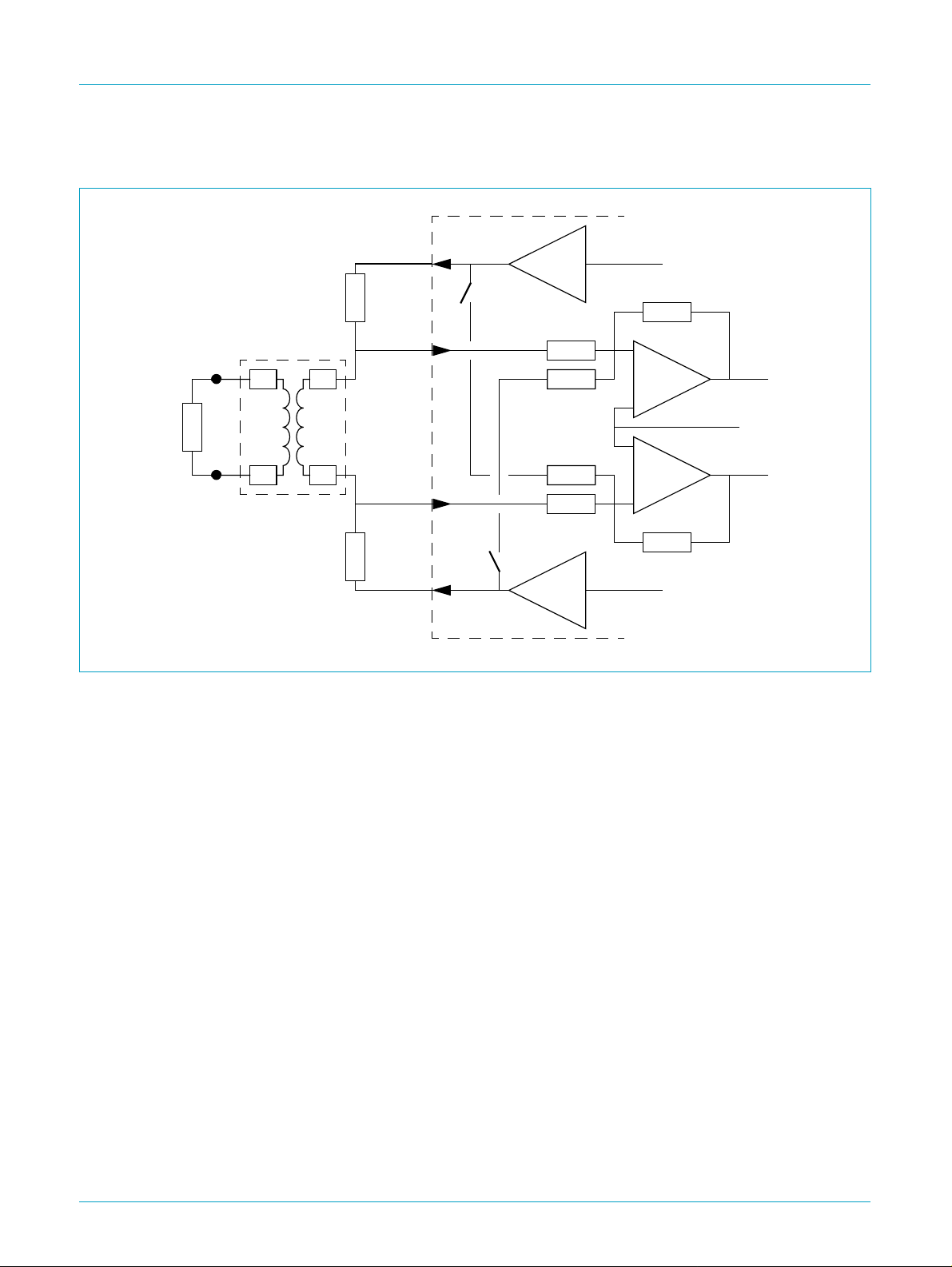
8.2 Analog interface
UCB1510
AC97 digital modem codec
UCB1510
TOUTP
A
Central Office
1:1 transformer
Rt
Rt
Ro
TINP
Ri
Rs
Rg
+
+
Rt
B
Fig 4. Typical telecom codec sidetone suppression circuit (without protection circuits).
Rt
TINN
Ro
TOUTN
An important built-in feature of the telecom codec is the sidetone suppression circuit.
The sidetone suppression circuit is activated when sidetone_enable of register 0x5A
is set.The sidetone suppression circuit subtracts part of the telecom output signal
from the telecom input signal. As a result the available dynamic range of the input
path can be more effectively utilized. If the sidetone suppression circuit is disabled,
the telecom input dynamic range can be largely occupied by the telecom output
signal.
Rs
Ri
-
Rg
The built-in side tone suppression circuit, shown in Figure 4, has a fixed subtraction
ratio, set be the resistors R
and Ri, which equals
s
600
⁄
. This ratio is calculated from
456
the following relations.
The impedance seen by the telephone line equals:
Z
line
2RtR
×=
RoRi×
++
----------------- -
t
RoRi+
, differential, in which Rtrepresents winding resistance
of the transformer, divided by 2. Assuming Ri >> Ro, then
R
line
RtRtRo600 2⁄ 300Ω==++=
single ended.
A typical transformer has 156 Ω winding impedance, thus Ro should be 144 Ω. The
ratio of the telecom input and output voltage is, therefore:
V
i(tel)
V
---------------------------------------
o(tel)
156 300 144++
156 300+
V
o(tel)
456
×=×=
-------- -
600
Proper sidetone suppression thus requires Rs/Ri to be Vi/Vo.
9397 750 06856
Preliminary specification Rev. 01 — 4 February 2000 7 of 32
© Philips Electronics N.V. 2000. All rights reserved.
Philips Semiconductors
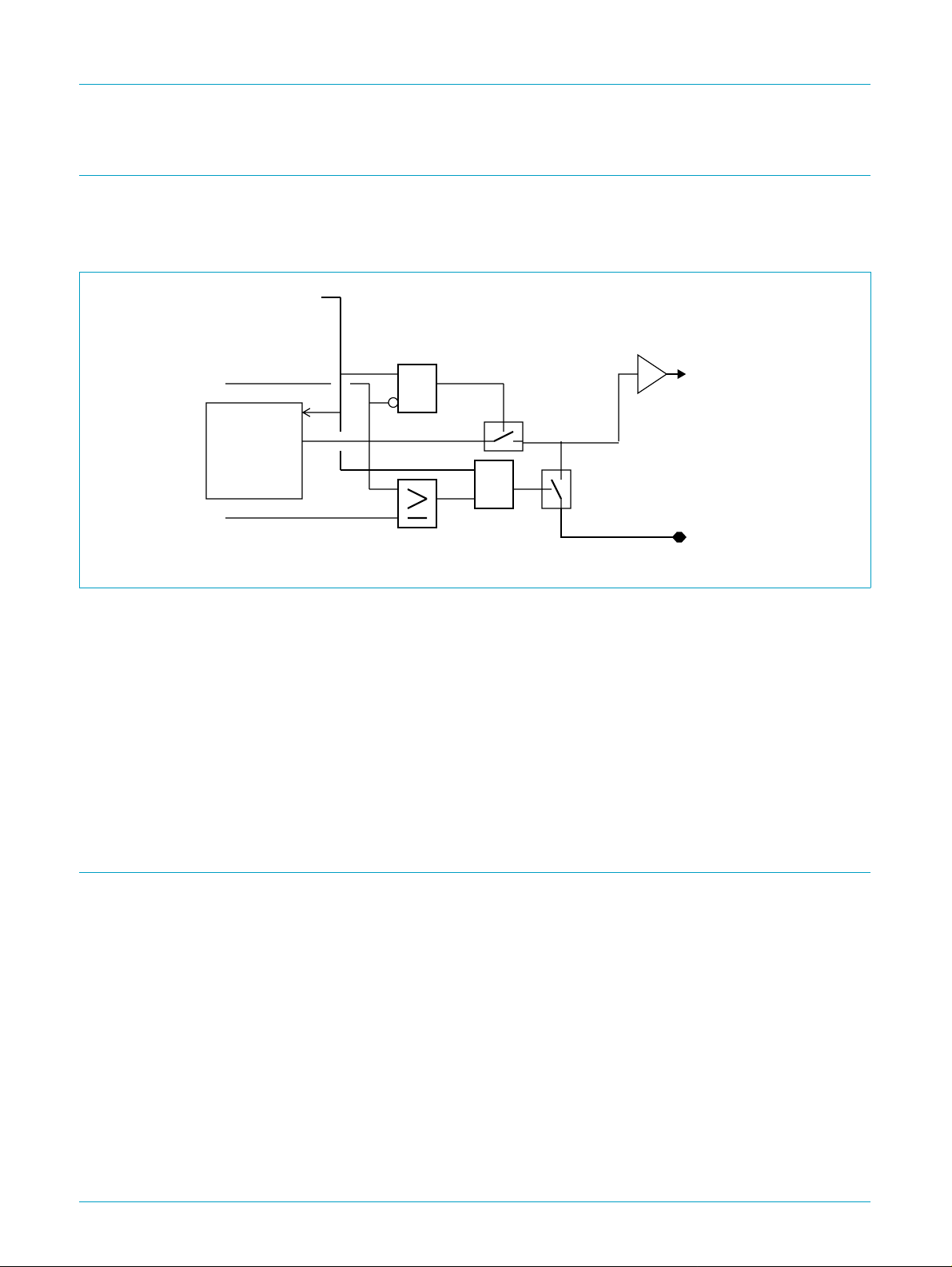
9. On-chip reference circuit
The UCB1510 contains an on chip reference voltage source, which generates the
bias currents and the virtual analog ground. Alternatively the UCB1510 can be driven
from an external reference voltage source.
Bias ENA
vref_external
ena
Vbg
vref_bypass
internal
bandgap
reference
voltage
circuitry
&
&
UCB1510
AC97 digital modem codec
internal
analog
ground
Fig 5. Block diagram of the reference circuit.
Two bits in the control register 0x5A determine the mode of operation of this
reference voltage circuit. vref_bypass connects the internal reference voltage to the
VREFBYP pin, while vref_external disables the internal reference voltage and
switches the UCB1510 into the external voltage reference mode.
If the internal reference voltage is connected to the VREFBYP pin, an external
capacitor could be connected to filter this reference voltage. When choosing a
capacitor, the internal impedance (around 50 kΩ) should be taken into account.
If vref_external is set, an external voltage reference connected to the VREFBYP pin
is used as the voltage reference by UCB1510.
10. Power supply strategy
Since all the control logic of the UCB1510 is powered by the V
alwaysbe present on this pin for interrupts to be possible. V
all the time although it is recommended to use the control bits to turn OFF the analog
sections.
VREFBYP
, power should
DDD
needs not be present
DDA
9397 750 06856
Preliminary specification Rev. 01 — 4 February 2000 8 of 32
© Philips Electronics N.V. 2000. All rights reserved.

Philips Semiconductors
11. Register definition
11.1 Supported registers
Table 5: Supported registers
Register Name
0x00 to 0x3A All audio registers are ignored
0x3C Extended Modem ID
0x3E Extended Modem Status and Control
0x40 Line1 DAC/ADC Rate
0x42 and 0x44 Reserved for future use
0x46 Line1 DAC/ADC Level
0x48 and 0x4A Reserved for future use
0x4C GPIO Pin Configuration
0x4E GPIO Pin Polarity
0x50 GPIO Pin Sticky
0x52 GPIO Pin Wake-up Mask
0x54 GPIO Pin Status
0x56 Miscellaneous Modem AFE Status and Control
0x58 Ignored
0x5A Codec control
0x5C Mode control
0x5E Test control
0x5E to 0x7A Ignored
0x7C Vendor ID1
0x7E Vendor ID2
UCB1510
AC97 digital modem codec
11.2 Register detail
Shaded areas indicate read only data.
11.2.1 Extended Modem ID
Table 6: Extended Modem ID Register
Register address: 0x3C; default: N/A
Bit D15 D14 D13 D12 D11 D10 D9 D8
Symbol
Bit D7 D6 D5 D4 D3 D2 D1 D0
Symbol
Table 7: Description of Extended Modem ID bits
Bit Symbol Function/Value
D15:14 ID[1:0] {A1,A0} where A0 is the inverse polarity of the
D0 LIN1 Line 1 support indicator = 1 (i.e., Line 1 is supported).
[1] Writing this register will cause a register reset: all modem registers will then take their default values.
9397 750 06856
Preliminary specification Rev. 01 — 4 February 2000 9 of 32
ID1 ID0
polarity of XTAL_IN pin if A0 is HIGH (
0 0 0 0 LIN1
A0 pin. A1 is the inverse
A0 pin is LOW), otherwise A1 is 0.
© Philips Electronics N.V. 2000. All rights reserved.

Philips Semiconductors
11.2.2 Extended Modem Status and Control
Table 8: Extended Modem Status and Control Register
Register address: 0x3E; default: 0xFFxx
Bit D15 D14 D13 D12 D11 D10 D9 D8
Symbol PRH PRG PRF PRE PRD PRC PRB PRA
Bit D7 D6 D5 D4 D3 D2 D1 D0
Symbol
Table 9: Description of Extended Modem status and Control bits
Bit Symbol Function/Value
D15 PRH Reserved, should be 1
D14 PRG Reserved, should be 1
D13 PRF Reserved, should be 1
D12 PRE Reserved, should be 1
D11 PRD 1 -> Line1 DAC OFF
D10 PRC 1 -> Line1 ADC OFF
D9 PRB 1 -> Line1 V
D8 PRA 1 -> GPIO OFF
D7 HDAC 0 (not supported)
D6 HADC 0 (not supported)
D5 DAC2 0 (not supported)
D4 ADC2 0 (not supported)
D3 DAC1 1 indicates Line1 DAC ready (means that the Line1 DAC and the V
D2 ADC1 1 indicates Line1 ADC ready (means that the Line1 ADC and the V
D1 MREF 1 indicates Line1 V
D0 GPIO 1 indicates GPIO ready.
UCB1510
AC97 digital modem codec
HDAC HADC DAC2 ADC2 DAC1 ADC1 MREF GPIO
OFF
REF
are enabled and ready)
are enabled and ready)
REF
up to nominal level.
REF
REF
11.2.3 Line 1 Sample Rate
Table 10: Line 1 Sample Rate Register
Register address: 0x40; default: 0x1F40
Bit D15 D14 D13 D12 D11 D10 D9 D8
Symbol SR15 SR14 SR13 SR12 SR11 SR10 SR9 SR8
Bit D7 D6 D5 D4 D3 D2 D1 D0
Symbol SR7 SR6 SR5 SR4 SR3 SR2 SR1 SR0
Refer to Table 3 “Sampling frequencies” for supported sample rates.
9397 750 06856
Preliminary specification Rev. 01 — 4 February 2000 10 of 32
© Philips Electronics N.V. 2000. All rights reserved.
 Loading...