

Philips ucb1300 DATASHEETS

INTEGRATED CIRCUITS
DATA SH EET
UCB1300
Advanced modem/audio analog
front-end
Product specification
Supersedes data of 1999 Jul 20
2000 Jun 26

Philips Semiconductors Product specification
Advanced modem/audio analog
front-end
FEATURES
• 48 pin LQFP (SOT313-2) small body SMD package and low external component count results in minimal PCB space
requirement
• 12-bit sigma delta audio codecwith programmable samplerate, input andoutput voltage levels, capable of connecting
directly to speaker and microphone, including digitally controlled mute, loopback and clip detection functions
• 14-bit sigma delta telecom codec with programmable sample rate, including digitally controlled input voltage level,
mute, loopback and clip detection functions. The telecom codec can be directly connected to a Data Access
Arrangement (DAA) and includes a built in sidetone suppression circuit
• Complete 4 wire resistive touch screen interface circuit supporting position, pressure and plate resistance
measurements
• 10-bit successive approximation ADC with internal track and hold circuit and analog multiplexer for touch screen
read-out and monitoring of four external high voltage (7.5V) analog voltages
• High speed, 4 wire serial interface data bus (SIB) for communication to the system controller
• 3.3V supply voltage and built in power saving modes make the UCB1300 optimal for portable and battery powered
applications
• Maximum operating current 25 mA
• 10 general purpose IO pins
APPLICATIONS
• Handheld Personal Computers, Personal Intelligent Communicators, Personal Digital Assistants
• Smart Mobile Phones
• Screen/Web Phones
• Internet Access Terminal
• Modems
UCB1300
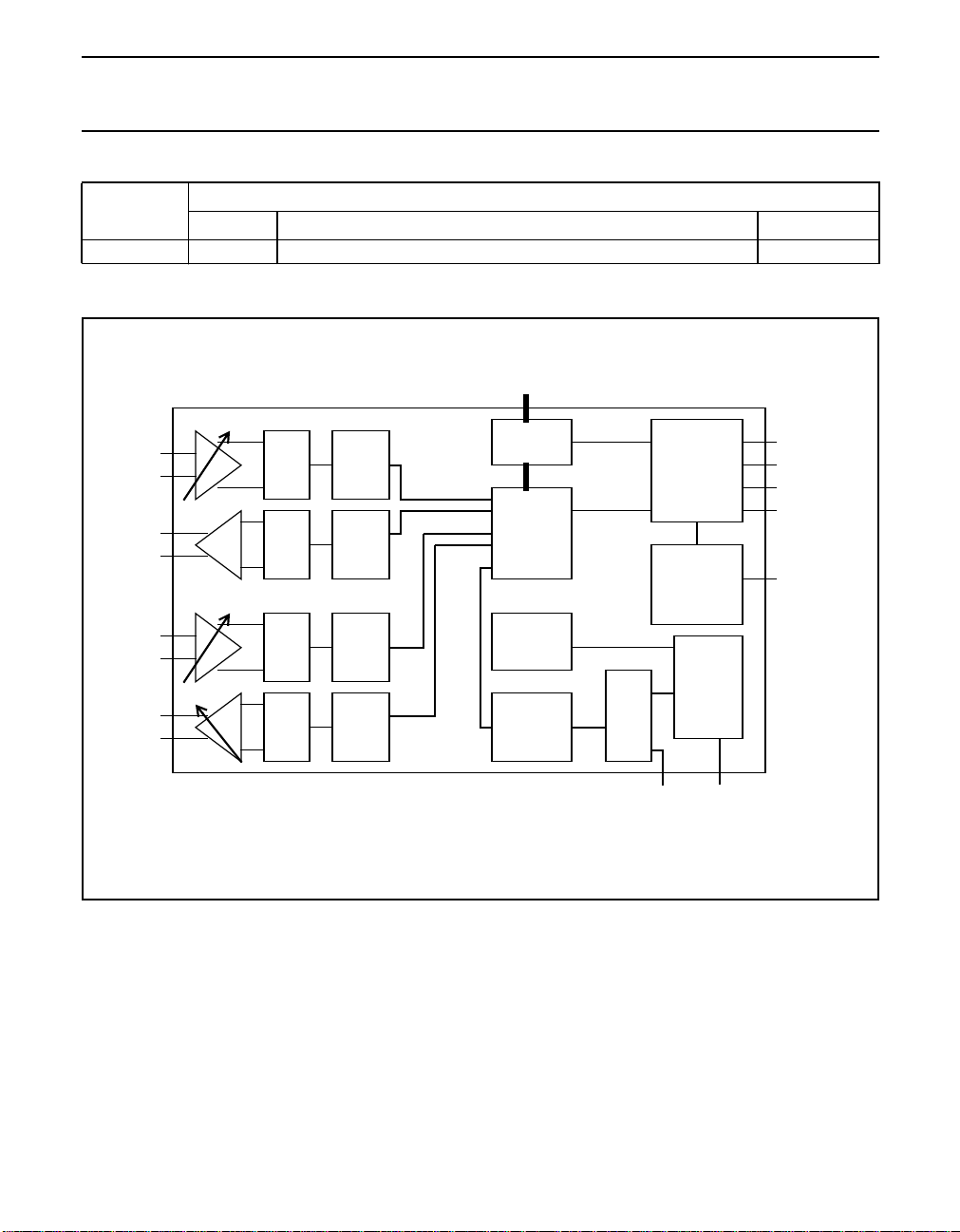
GENERAL DESCRIPTION
The UCB1300 is a single chip, integrated mixed signal audio and telecom codec. The single channel audio codec is
designed for direct connection of a microphone and a speaker. The built-in telecom codec can directly be connected to
a DAA and supports high speed modem protocols. The incorporated analog-to-digital converter and the touch screen
interface provides complete control and read-out of an 4 wire resistive touch screen. The 10 general purpose I/O pins
provide programmable inputs and/or outputs to the system.
The UCB1300 has a serial interface bus (SIB) intended to communicate to the system controller. Both the codec input
data and codec output data and the control register data are multiplexed on this SIB interface.
2000 Jun 26 2 853-220023989
Philips Semiconductors Product specification
Advanced modem/audio analog front-end UCB1300
ORDERING INFORMATION
TYPE
NUMBER
NAME DESCRIPTION VERSION
UCB1300BE LQFP48 plastic low profile quad flat package; 48 leads; body 7 × 7 × 1.4 mm SOT313-2
BLOCK DIAGRAM
PACKAGE
IO(n)
TINP
TINN
TOUTP
TOUTN
MICP
MICGND
SKRP
SKRN
1 bit
ADC
4 bit
DAC
1 bit
ADC
4 bit
DAC
down
sample
filter
up
sample
filter
down
sample
filter
up
sample
filter
Digital IO
circuits
data /
control
registers
Voltage
reference
10 bit ADC
Fig.1 Block diagram.
Serial bus
interface
Clock buffers &
sample rate
dividers
multiplexer
AD(n)
touch
screen
interface
SIBDIN
SIBDOUT
SIBSYNC
IRQOUT
SIBCLK
TSPX,TSMX
TSPY,TSMY
2000 Jun 26 3

Philips Semiconductors Product specification
Advanced modem/audio analog front-end UCB1300
PINNING
SYMBOL PIN DESCRIPTION
RESET
STATE
IO7 1 general purpose I/O pins input I/O
IO8 2 general purpose I/O pins input I/O
IO9 3 general purpose I/O pins input I/O
ADCSYNC 4 ADC synchronization pulse input - I
V
SSD
5 digital ground - S
n.c 6 not connected - V
SSA2
7 analog speaker driver ground - S
SPKRN 8 negative speaker output Hi-Z O
SPKRP 9 positive speaker output Hi-Z O
V
DDA2
10 analog speaker driver supply - S
TOUTP 11 positive telecom codec output Hi-Z O
TOUTN 12 negative telecom codec output Hi-Z O
TEST 13 test mode protection ‘0’ I
TINN 14 negative telecom codec input Hi-Z I
TINP 15 positive telecom codec input Hi-Z I
VREFBYP 16 external reference voltage input Hi-Z I/O
V
V
DDA1
SSA1
17 analog supply - S
18 analog ground - S
n.c 19 not connected - MICGND 20 microphone ground switch input Hi-Z I
MICP 21 microphone signal input Hi-Z I
AD3 22 analog voltage inputs Hi-Z I
AD2 23 analog voltage inputs Hi-Z I
AD1 24 analog voltage inputs Hi-Z I
AD0 25 analog voltage inputs Hi-Z I
V
SSA3
26 analog touch screen ground - S
TSPY 27 positive Y-plate touch screen Hi-Z I/O
TSMX 28 negative X-plate touch screen Hi-Z I/O
TSMY 29 negative Y-plate touch screen Hi-Z I/O
TSPX 30 positive X-plate touch screen Hi-Z I/O
n.c 31 not connected - V
DDD
32 digital supply - S
IO0 33 general purpose I/O pins input I/O
IO1 34 general purpose I/O pins input I/O
IO2 35 general purpose I/O pins input I/O
IO3 36 general purpose I/O pins input I/O
V
SSD
37 digital ground - S
RESET 38 asynchronous reset input - I
SIBSYNC 39 SIB synchronization input - I
TYPE
C
C
C
C
(2)
A
A
A
A
C
A
A
A
A
A
A
A
A
A
A
A
A
A
C
C
C
C
C
C
(1)
2000 Jun 26 4
Philips Semiconductors Product specification
Advanced modem/audio analog front-end UCB1300
SYMBOL PIN DESCRIPTION
SIBDOUT 40 SIB data output ‘1’
RESET
STATE
(6)
SIBCLK 41 SIB serial interface clock − I
SIBDIN 42 SIB data input − I
IRQOUT 43 interrupt output ‘0’ O
TYPE
O
C
C
C
C
(1)
n.c 44 not connected −−
IO4 45 general purpose I/O pins input I/O
IO5 46 general purpose I/O pins input I/O
IO6 47 general purpose I/O pins input I/O
V
DDD
48 digital supply − S
C
C
C
Notes
1. I/OC= CMOS bidirectional; ID= digital input; S = supply; OA= analog output; IC= CMOS input; IA= analog input;
I/OA= analog bidirectional; OC= CMOS output.
2. V
(pins 5 and 37) and V
SSD
(pin 18) are connected internally within the UCB1300.
SSA1
3. SKPRN/SPKRP (pins 8 and 9), TINN/TINP (pins 14 and 15) and TOUTP/TOUTN are differential pairs
4. TEST (pin 13) is connected to an internal pull-down resistor. This pin should be held LOW during normal operation
of the circuit.
5. The ‘not connected’ pins (pins 6, 19, 31 and 44) are reserved for future applications and should be left floating.
6. SIBDOUT reset state is 1 until the SIB bus is running. SIBDOUT will be active once the SIB bus has started.
2000 Jun 26 5

Philips Semiconductors Product specification
Advanced modem/audio analog front-end UCB1300
book, full pagewidth
IO7
IO8
IO9
ADCSYNC
V
SSD
n.c.
V
SSA2
SPKRN
SPRKP
V
DDA2
TOUTP
TOUTN
DDD
V
1
2
3
4
5
6
7
8
9
10
11
12
TEST
IO5
IO6
48
47
46
13
14
15
TINP
TINN
n.c.
IO4
45
44
UCB1300
16
17
DDA1VSSA1
V
IRQOUT
43
XXX
18
VREFBYP
SIBCLK
SIBDIN
42
41
19
20
n.c.
MICGND
SIBDOUT
40
21
MICP
RESET
SIBSYNC
39
38
22
23
AD3
AD2
SSD
V
37
24
AD1
36
35
34
33
32
31
30
29
28
27
26
25
MXXxxx
IO3
IO2
IO1
IO0
V
DDD
n.c.
TSPX
TSMY
TSMX
TSPY
V
SSA3
AD0
Fig.2 Pin configuration.
2000 Jun 26 6

Philips Semiconductors Product specification
Advanced modem/audio analog front-end UCB1300
FUNCTIONAL DESCRIPTION
The UCB1300 consists of several analog and digital sub-circuits which can be programmed via the Serial Interface Bus
(SIB). This enables the user to set the UCB1300 functionality according to actual application requirements.
AUDIO CODEC
The audio codec contains an input channel, built up with a 64 timesoversampling sigma delta analog todigital converter
(ADC) with digital decimation filters and a programmable gain microphone preamplifier. The programmable gain
microphone amplifier features a built-in offset cancellation stage, which reduces the distortion of this stage at high gain
settings, caused by the offset voltages of the internal amplifiers or leakage on the board. It can be deactivated (reg13,
bit 13) for improved performance at low gain settings. A general rule is that below a gain setting of 16 (24dB gain) the
offset cancellation circuit will reduce THD and signal bandwidth and should then be deactivated.
The output path consists of a digital up-sample filter, a 64 time oversampling 4-bit digital-to-analog converter (DAC)
circuit followed by a BTL speaker driver, capable of driving a 16 Ω speaker. The output path features a digital
programmable attenuation and a mute function.
The audio codec also incorporates a loopback mode, in which codec output path and the input path are connected in
series.
2000 Jun 26 7
Philips Semiconductors Product specification
Advanced modem/audio analog front-end UCB1300
AUD_GAIN[4,3] AUD_OFF_CAN AUD_LOOP AUD_GAIN[2..0]
MICP
MICGND
VCCSPKR
SPKRP
SPKRN
VSSSPKR
AUD_MUTE AUD_ATT[2..0]
Fig.3 Audio codec block diagram.
4-bit DAC
1-bit ADC
DIGITAL
ATTENUATOR
AUD_ATT[4,3]
DIGITAL
DECIMATION
FILTER
AUD_IN_ENA
AUD_OUT_ENA
DIGITAL
NOISE
SHAPER
12
12
The audio sample rate (fsa) is derived from the SIB interface clock pin (SIBCLK) and is programmable through the SIB
interface using AUD_DIV[n]. The audio sample rate is given by the following equation:
2f
×()
f
=
sa
SIBCLK
-------------------------------------------------64 AUD_DIV[n]×()
(7< AUD_DIV[n] < 128)
For example,a serial clock of 9.216 MHz, with a divisorof 12, results inan audio sample rate of 24.0 kHz. Both therising
and the falling edges of SIBCLK are usedin case AUD_DIV[n]is set toan odd number,which demands a50% duty cycle
of SIBCLK to obtain time equidistant sampling.
2000 Jun 26 8

Philips Semiconductors Product specification
Advanced modem/audio analog front-end UCB1300
V
DDA1
17
MICP
21
MICGND
20
V
SSA1
18
PASSIVE
UCB1300 UCB1300
V
DDA1
MICGND
17
MICP
21
20
V
SSA1
18
ACTIVE
Fig.4 Possible microphone connections.
The UCB1300audio codec inputpath accepts microphone signalsdirectly, only a DC blocking capacitor isneeded since
the MICP input is biased around 1.4V. The ‘ground’ side of the microphone is either connected to the analog ground
(V
) or to the MICGND pin. The latter will decrease the current consumption of active microphones, since the
SSA1
MICGND pin is made Hi-Z when the audio codec input path is disabled.
The full scale input voltage of the audio input path is programmable in1.5 dB steps by setting the appropriate number in
AUDIO_GAIN[n] in the audio control register A. Using very high gains may require the use of the internal offset
cancellation circuit programmable in reg 13 to avoid clipping in the ADC.
A clipdetection circuit will inform theuser whenever the input voltage exceeds the maximum inputvoltage, since this will
lead to a high distortion. In that case AUD_CLIP_STAT in the audio control register B is set. When ACLIP_RIS_INT is
set, an interrupt is generated on the IRQOUT pin on the rising edge of the clip detect signal. When ACLIP_FAL_INT is
set, an interrupt is generated on the falling edge of the clip detect signal.
The frequency response of the audio codec depends mainly on the selected sample rate, since the bandwidth is limited
in the down and up sampling filters. These digital filters both contain several FIR and IIR low pass filters and a DC
removal filter(high pass filter). A third-order smoothing filter is implemented in the DAC path,between DAC and speaker
driver stage to reduce the spurious frequencies at the speaker outputs.
2000 Jun 26 9
Philips Semiconductors Product specification
Advanced modem/audio analog front-end UCB1300
48dB
24dB
0dB
21dB
0dB
24dB
programmed attenuation
48dB 69dB
Fig.5 Analog and digital attenuation settings audio output path.
The output level can be attenuated in 3 dB steps down to -69 dB. The first 8 attenuation steps (0 to 21 dB) are
implemented in the analog domain. The digital up sample filter contains a 24 dB and a 48 dB attenuation setting. This
arrangement preservesthe resolution, thus the ‘audio quality’ of the audio output signal for attenuationsettings till 21 dB.
The speaker driver is muted when AUDIO_MUTE in the audio control register B is set. The speaker driver will remain
activated in that case, however no signal is produced by the speaker driver circuit.
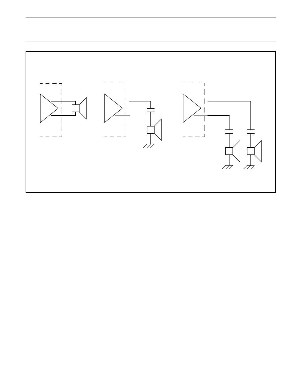
The speaker driver is designed to directly drive a Bridge Tied Load (BTL). This yields the highest output power and this
arrangementdoes notrequire external DC blocking capacitors.The speakerdriver alsoaccepts single-endedconnection
of a speaker, in which case the maximum output power is reduced to a quarter of the BTL situation. Consequently this
way of connecting the speaker to the speaker driver reduces the power consumption of the speaker driver in the
UCB1300 by a factor of 2. Fig.6 shows possible ways to connect a speaker to the driver. Loading the amplifiers with a
capacitive load may cause high frequency oscillations and should be done cautiously.
2000 Jun 26 10
Philips Semiconductors Product specification
Advanced modem/audio analog front-end UCB1300
BRIDGE TIED
SPEAKER LOAD
UCB1300 UCB1300 UCB1300
SPKRP
9
+
8
SPKRN
SINGLE-ENDED SPEAKER CONNECTIONS
SPKRP
9
8
SPKRN
SPKRP
9
8
SPKRN
+
+
Fig.6 Possible speaker connections.
The audioinput and outputpath are activated independently.The input pathis enabled when AUDIO_IN_ENAis set, the
output path is enabled when AUD_OUT_ENA is set in the audio control register B. This provides the user the means to
reduce the current consumption of the UCB1300 if one part of the audio codec is not used in the application.
The audio codec has a loopback mode for system test purposes, which is activated when the AUDIO_LOOP bit in the
audio control register B is set. This is an analog loopback which internally connects the output of the audio output path
to the input of the audio input path, (see Fig.3). In this mode the normal microphone input is ignored, but the speaker
driver can be operated normally.
+
2000 Jun 26 11
Philips Semiconductors Product specification
Advanced modem/audio analog front-end UCB1300
TELECOM CODEC
The telecom codec contains an input channel, built up from a 64 times oversampling sigma delta analog-to-digital
converter (ADC) with digital decimation filters, programmable attenuation gain and built-in sidetone suppression circuit.
The output path consist of a digital up-sample filter, a 64 times oversampling 4-bit digital-to-analog converter (DAC)
circuit followed by a differential output driver, capable of directly driving a 600 Ω isolation transformer. The output path
includes a mute function. The telecom codec also incorporates a loopback mode, in which codec output path and the
input path are connected in series.
TOUTP
TOUTN
TINP
TINN
TEL_SIDE_ENA
SIDETONE
SUPPRESSION
CIRCUIT
TEL_MUTE
TEL_ATTATT TEL_GAIN
1-bit ADC
4-bit DAC
DIGITAL
DECIMATION
FILTER
TEL_IN_ENA
TEL_OUT_ENA
DIGITAL
NOISE
SHAPER
14
14
Fig.7 Telecom codec block diagram.
The telecom sample rate (fst) is derived from the SIB interface clock pin (SIBCLK) and is programmable through the SIB
interface. The telecom sample rate is given by the following formula:
2F
×()
f
=
------------------------------------------------- -
st
SIBCLK
64 TEL_DIV[n]×()
(15 < TEL_DIV[n] <128)
For example, a SIBCLK of 9.216 MHz, with a divisor of 40, results in a telecom sample rate of 7.2 kHz. Both the rising
and the falling edges of the SIBCLK are usedin case TEL_DIV[n] is set to an odd number. In that case a 50% duty cycle
of the SIBCLK signal is mandatory to obtain time equidistant sampling.
The input path of the telecom codec has a programmable attenuation gain. It also implements a voice band filter, which
consists ofa digital low pass filter,which is a part of the decimation filter. Therefore the pass band of the voice band filter
2000 Jun 26 12

Philips Semiconductors Product specification
Advanced modem/audio analog front-end UCB1300
is determinedby the selectedtelecom codec sample rate.This voice bandfilter is activated bysetting TEL_VOICE_ENA
in the telecom control register B. The resulting telecom input filter curves are given in Fig.38 and Fig.39.
The output section of the telecom codec is designed to interface with a 600 Ω line through an isolation transformer. The
built-in mutefunction is activated byTEL_MUTE in the telecom control register B. The output driver remainsactive in the
mute mode, howeverno output signal is produced. Loading the drivers with a capacitive load may cause high frequency
oscillations and should be done cautiously.
2000 Jun 26 13
Philips Semiconductors Product specification
Advanced modem/audio analog front-end UCB1300
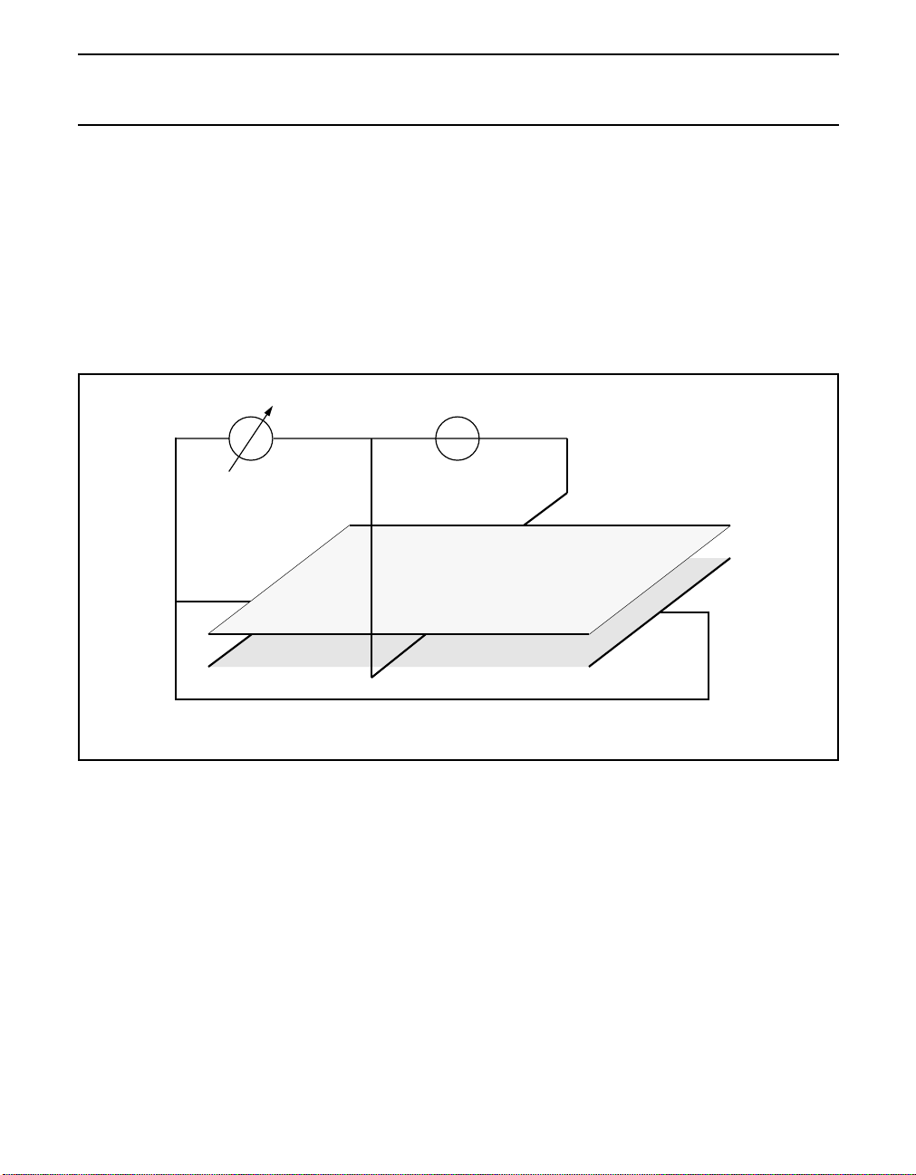
TOUCH SCREEN MEASUREMENT MODES
The UCB1300 contains an on-chip interface for a 4 wire resistive touch screen. This interface supports three modes of
touch screen measurements: position, pressure and plate resistance.
POSITION MEASUREMENT
Twoposition measurementsare needed to determine thelocation ofthe pressedspot. Firstan Xmeasurement, secondly
a Y measurement. The Xplate is biasedduring the X position measurement of theX plate andthe voltage onone or both
Y terminals (TSPY, TSMY) measured. The circuit can then be represented by a potentiometer, with the TSPY and/or
TSMY electrode being the ‘wiper’. The measured voltage on the TSPY/TSMY terminal is proportional to the X position
of the pressed spot of the touch screen.
Vposition
Vtscbias
tspx
tsmy
tspy
tsmx
Fig.8 Touch screen setup for position measurement.
In the Y position mode the X plate and Y plate terminals are interchanged, thus the Y plate is biased while the voltage
on the TSPX and/or TSMX terminal is measured.
2000 Jun 26 14
Philips Semiconductors Product specification
Advanced modem/audio analog front-end UCB1300
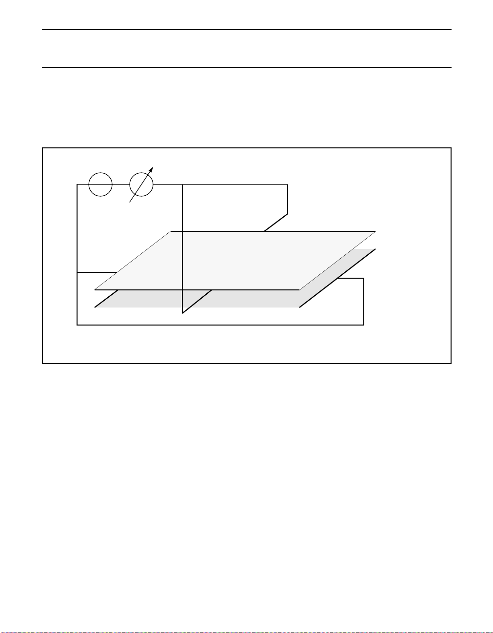
PRESSURE MEASUREMENT
The pressure used to press the touch screen can be determined. In fact, the contact resistance between the X and Y
plate is measured, which is a good indication of the size of the pressed spot and the applied pressure. A soft stylus, e.g.
a finger, leads to a rather large contact area between the two plates when a large pressure is applied. A hard stylus, e.g.
a pen, leads to less variation in measured contact resistance since the contact area is rather small.
Vtscbias
ipressure
tspx
tsmy
tspy
tsmx
Fig.9 Touch screen setup for pressure measurement.
One plate is biased at one or both terminals during this pressure measurement, whereas the other plate is grounded,
again on one or both terminals. The current flowing through the touch screen is a direct indication for the resistance
between both plates. A compensation for the series resistance, formed by the touch screen plates itself will improve the
accuracy ofthis measurement. The measurement is done with a resistive voltage divider. The internalresistor should be
taken into account to evaluate the settling time of the pressure measurement given the board capacitors connected to
the ADC tap point in pressure mode.
2000 Jun 26 15
Philips Semiconductors Product specification
Advanced modem/audio analog front-end UCB1300
Vtscbias
Measured resistor
Switch matrix
To ADC
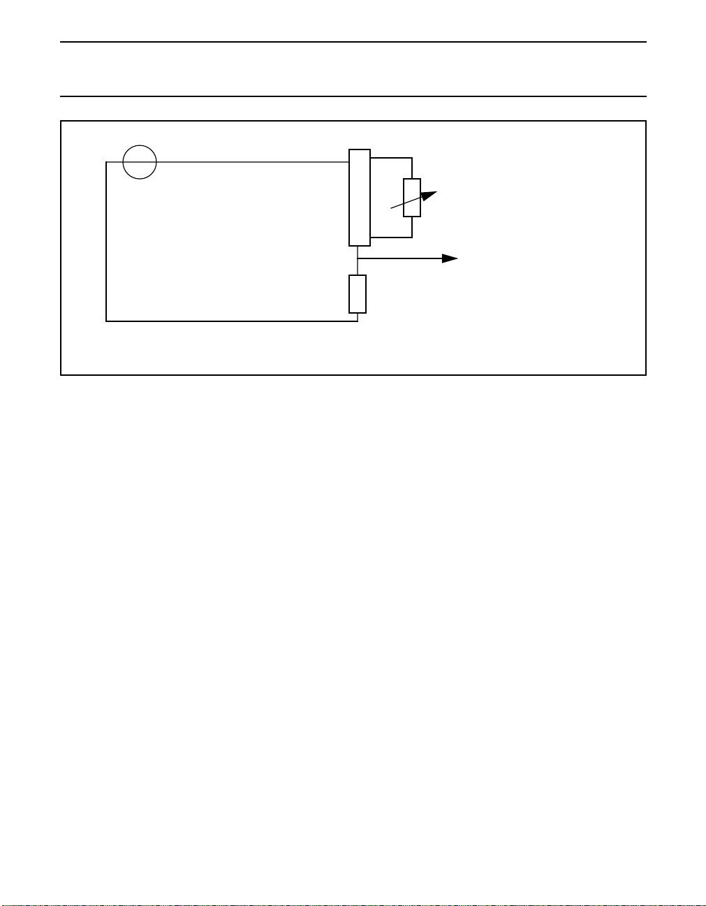
Internal resistor (about 1kΩ)
Fig.10 Pressure measurement scheme.
2000 Jun 26 16

Philips Semiconductors Product specification
Advanced modem/audio analog front-end UCB1300
PLATE RESISTANCE MEASUREMENT
Theplate resistance of a touchscreen typicallyvaries alot due to processing spread.Knowing theactual plateresistance
makes it possible to compensate for the plate resistance effects in pressure resistance measurements. The plate
resistance decreases when two or more spots on the touch screen are pressed.In that case, a part of one plate, e.g. the
X plate, is shorted by the other plate, which decreases the actual plate resistance
Vtscbias
iplate
tspx
tsmy
tspy
tsmx
Fig.11 Touch screen setup for plate resistance.
The plate resistance measurement is executed in the same way as the pressure resistance measurement. In this case
only one of the two plates is biased and the other plate is kept floating. The current through the connected plate is again
a direct indication of the connected resistance.
2000 Jun 26 17
 Loading...