

Philips ucb1200 DATASHEETS

INTEGRATED CIRCUITS
DATA SH EET
UCB1200
Advanced modem/audio analog
front-end
Product specification
File under Integrated Circuits, <Handbook>
1998 Jul 22

Philips Semiconductors Product specification
Advanced modem/audio analog
front-end
FEATURES
• 48 pin LQFP (SOT313) small body SMD package and low external component count results in minimal PCB space
requirement
• 12-bit sigma delta audiocodec with programmable sample rate,input andoutput voltage levels,capable ofconnecting
directly to speaker and microphone, including digitally controlled mute, loopback and clip detection functions
• 14-bit sigma delta telecom codec with programmable sample rate, including digitally controlled input voltage level,
mute, loopback and clip detection functions. The telecom codec can be directly connected to a Data Access
Arrangement (DAA) and includes a built in sidetone suppression circuit
• Complete 4 wire resistive touch screen interface circuit supporting position, pressure and plate resistance
measurements
• 10-bit successive approximation ADC with internal track and hold circuit and analog multiplexer for touch screen
read-out and monitoring of four external high voltage (7.5V) analog voltages
• High speed, 4 wire serial interface data bus (SIB) for communication to the system controller
• 3.3V supply voltage and built in power saving modes make the 9397 750 04055 optimal for portable and battery
powered applications
• Maximum operating current 25 mA
• 10 general purpose IO pins
APPLICATIONS
• Handheld Personal Computers, Personal Intelligent Communicators, Personal Digital Assistants
• Smart Mobile Phones
• Screen/Web Phones
• Internet Access Terminal
• Modems
UCB1200
GENERAL DESCRIPTION
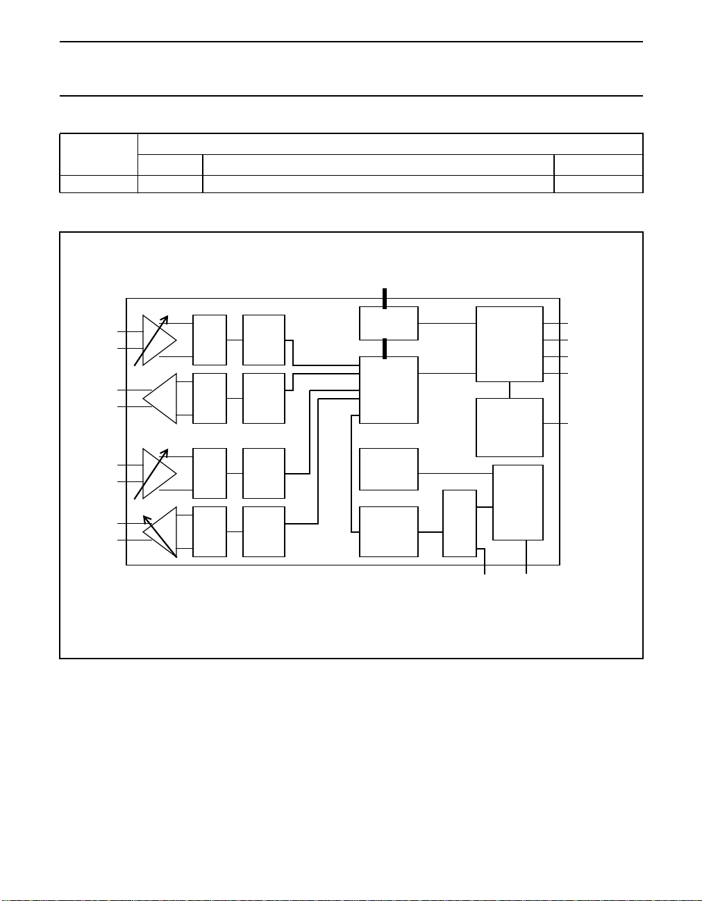
The UCB1200 is a single chip, integrated mixed signal audio and telecom codec. The single channel audio codec is
designed for direct connection of a microphone and a speaker. The built-in telecom codec can directly be connected to
a DAA and supports high speed modem protocols. The incorporated analog to digital converter and the touch screen
interface provides complete control and read-out of an 4 wire resistive touch screen. The 10 general purpose I/O pins
provide programmable inputs and/or outputs to the system.
The UCB1200 has a serial interface bus (SIB) intended to communicate to the system controller. Both the codec input
data and codec output data and the control register data are multiplexed on this SIB interface.
1998 Jul 22 2 853-205219059
Philips Semiconductors Product specification
Advanced modem/audio analog front-end UCB1200
ORDERING INFORMATION
TYPE
NUMBER
NAME DESCRIPTION VERSION
UCB1200BE LQFP48 plastic low profile quad flat package; 48 leads; body 7 × 7 × 1.4 mm SOT313-2
BLOCK DIAGRAM
PACKAGE
IO(n)
TINP
TINN
TOUTP
TOUTN
MICP
MICGND
SKRP
SKRN
1 bit
ADC
4 bit
DAC
1 bit
ADC
4 bit
DAC
down
sample
filter
up
sample
filter
down
sample
filter
up
sample
filter
Digital IO
circuits
data /
control
registers
Voltage
reference
10 bit ADC
Fig.1 Block diagram.
Clock buffers &
sample rate
multiplexer
AD(n)
Serial bus
interface
dividers
touch
screen
interface
SIBDIN
SIBDOUT
SIBSYNC
IRQOUT
SIBCLK
TSPX,TSMX
TSPY,TSMY
1998 Jul 22 3

Philips Semiconductors Product specification
Advanced modem/audio analog front-end UCB1200
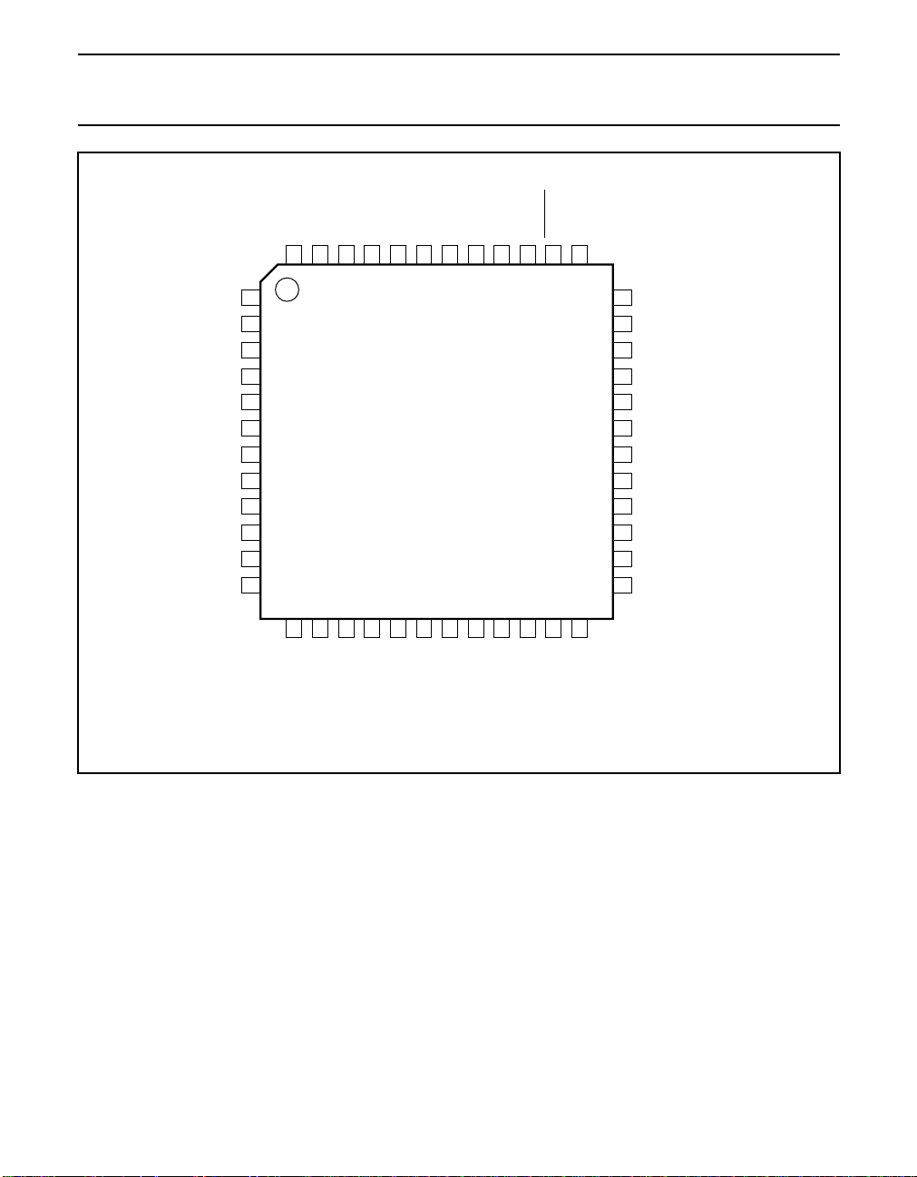
PINNING
SYMBOL PIN DESCRIPTION
RESET
STATE
IO7 1 general purpose I/O pins input I/O
IO8 2 general purpose I/O pins input I/O
IO9 3 general purpose I/O pins input I/O
ADCSYNC 4 ADC synchronization pulse input − I
V
SSD
5 digital ground − S
n.c 6 not connected −−
V
SSA2
7 analog speaker driver ground − S
SKPRN 8 negative speaker output hi Z O
SPRKP 9 positive speaker output hi Z O
V
DDA2
10 analog speaker driver supply − S
TOUTP 11 positive telecom codec output hi Z O
TOUTN 12 negative telecom codec output hi Z O
TEST 13 test mode protection ‘0’ I
TINN 14 negative telecom codec input hi Z I
TINP 15 positive telecom codec input hi Z I
VREFBYP 16 external reference voltage input hi Z I/O
V
V
DDA1
SSA1
17 analog supply − S
18 analog ground − S
n.c 19 not connected −−
MICGND 20 microphone ground switch input hi Z I
MICP 21 microphone signal input hi Z I
AD3 22 analog voltage inputs hi Z I
AD2 23 analog voltage inputs hi Z I
AD1 24 analog voltage inputs hi Z I
AD0 25 analog voltage inputs hi Z I
V
SSA3
26 analog touch screen ground − S
TSPY 27 positive Y-plate touch screen hi Z I/O
TSMX 28 negative X-plate touch screen hi Z I/O
TSMY 29 negative Y-plate touch screen hi Z I/O
TSPX 30 positive X-plate touch screen hi Z I/O
n.c 31 not connected −−
V
DDD
32 digital supply − S
IO0 33 general purpose I/O pins input I/O
IO1 34 general purpose I/O pins input I/O
IO2 35 general purpose I/O pins input I/O
IO3 36 general purpose I/O pins input I/O
V
SSD
37 digital ground − S
RESET 38 asynchronous reset input − I
SIBSYNC 39 SIB synchronization input − I
TYPE
C
C
C
C
(2)
A
A
A
A
C
A
A
A
A
A
A
A
A
A
A
A
A
A
C
C
C
C
C
C
(1)
1998 Jul 22 4
Philips Semiconductors Product specification
Advanced modem/audio analog front-end UCB1200
SYMBOL PIN DESCRIPTION
SIBDOUT 40 SIB data output ‘1’
RESET
STATE
(6)
SIBCLK 41 SIB serial interface clock − I
SIBDIN 42 SIB data input − I
IRQOUT 43 interrupt output ‘0’ O
TYPE
O
C
C
C
C
(1)
n.c 44 not connected −−
IO4 45 general purpose I/O pins input I/O
IO5 46 general purpose I/O pins input I/O
IO6 47 general purpose I/O pins input I/O
V
DDD
48 digital supply − S
C
C
C
Notes
1. I/OC= CMOS bidirectional; ID= digital input; S = supply; OA= analog output; IC= CMOS input; IA= analog input;
I/OA= analog bidirectional; OC= CMOS output.
2. V
(pins 5 and 37) and V
SSD
(pin 18) are connected internally within the UCB1200.
SSA1
3. SKPRN/SPKRP (pins 8 and 9), TINN/TINP (pins 14 and 15) and TOUTP/TOUTN are differential pairs
4. TEST (pin 13) is connected to an internal pull-down resistor. This pin should be held LOW during normal operation
of the circuit.
5. The not connected pins (pins 6, 19, 31 and 44) are reserved for future applications and should be left floating.
6. SIBDOUT reset state is 1 until the SIB bus is running. SIBDOUT will be active once the SIB bus has started.
1998 Jul 22 5
Philips Semiconductors Product specification
Advanced modem/audio analog front-end UCB1200
book, full pagewidth
IO7
IO8
IO9
ADCSYNC
V
SSD
n.c.
V
SSA2
SPKRN
SPRKP
V
DDA2
TOUTP
TOUTN
DDD
V
1
2
3
4
5
6
7
8
9
10
11
12
TEST
IO5
IO6
48
47
46
13
14
15
TINP
TINN
n.c.
IO4
45
44
UCB1200
16
17
DDA1VSSA1
V
IRQOUT
43
XXX
18
VREFBYP
SIBCLK
SIBDIN
42
41
19
20
n.c.
MICGND
SIBDOUT
40
21
MICP
RESET
SIBSYNC
39
38
22
23
AD3
AD2
SSD
V
37
24
AD1
36
35
34
33
32
31
30
29
28
27
26
25
MXXxxx
IO3
IO2
IO1
IO0
V
DDD
n.c.
TSPX
TSMY
TSMX
TSPY
V
SSA3
AD0
Fig.2 Pin configuration.
1998 Jul 22 6

Philips Semiconductors Product specification
Advanced modem/audio analog front-end UCB1200
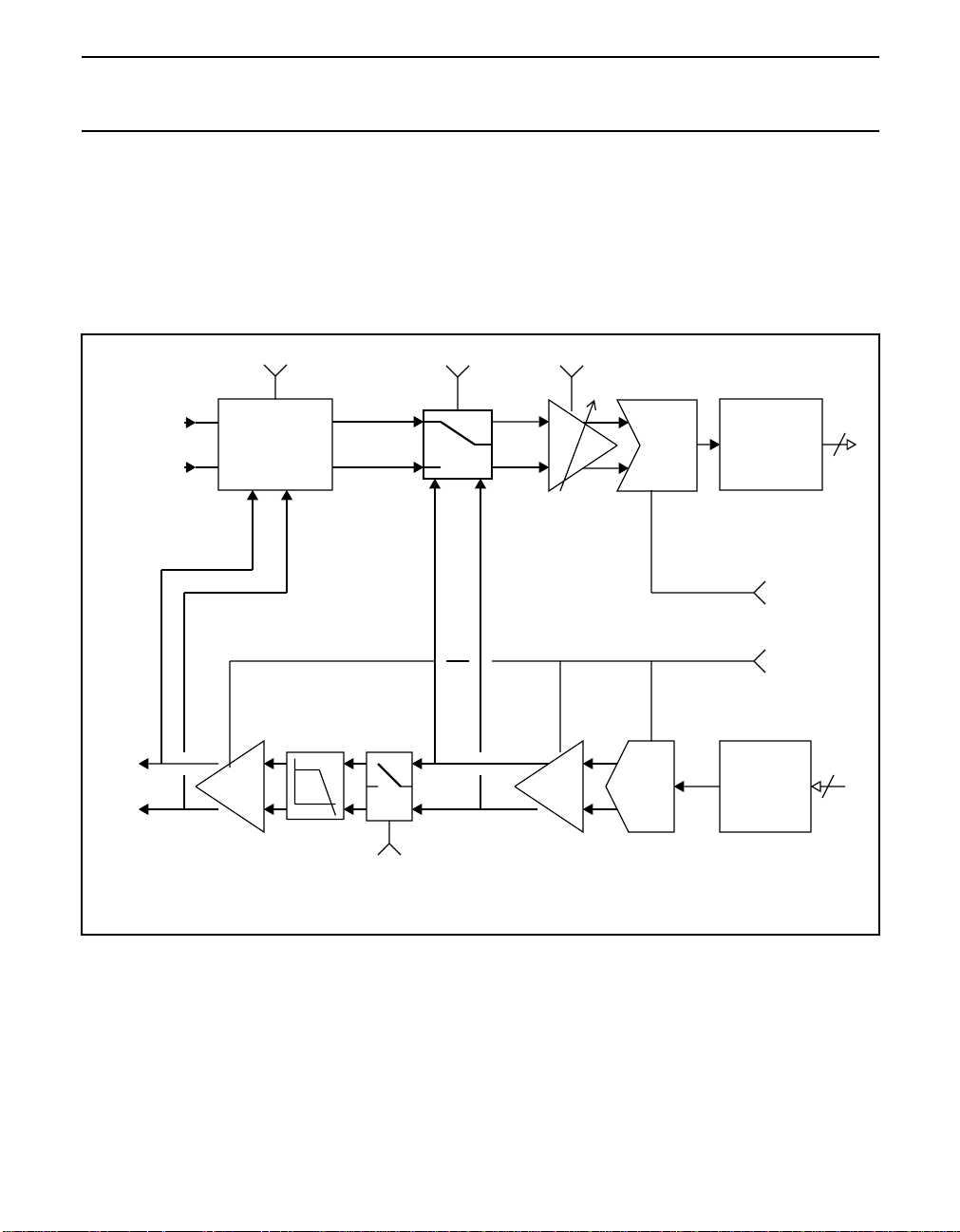
FUNCTIONAL DESCRIPTION
The UCB1200 consists of several analog and digital sub circuits which can be programmed via the Serial Interface Bus
(SIB). This enables the user to set the UCB1200 functionality according to actual application requirements.
AUDIO CODEC
Theaudio codeccontains aninput channel,built upwith an64 timesoversampling sigmadelta analogto digitalconverter
(ADC) with digital decimation filters and a programmable gain microphone preamplifier.
The output path consistsof adigital up sample filter, a64 timeoversampling 4 bit digital toanalog converter(DAC) circuit
followed by a BTL speaker driver, capable of driving a 16 Ω speaker. The output path features a digital programmable
attenuation and a mute function.
The audio codec also incorporates a loopback mode, in which codec output path and the input path are connected in
series.
AUD_GAIN[4,3] AUD_OFF_CAN AUD_LOOP AUD_GAIN[2..0]
MICP
MICGND
VCCSPKR
SPKRP
SPKRN
VSSSPKR
AUD_MUTE AUD_ATT[2..0]
Fig.3 Audio codec block diagram.
4bit DAC
1bit ADC
DIGITAL
ATTENUATOR
AUD_ATT[4,3]
DIGITAL
DECIMATION
FILTER
AUD_IN_ENA
AUD_OUT_ENA
DIGITAL
NOISE
SHAPER
12
12
1998 Jul 22 7
Philips Semiconductors Product specification
Advanced modem/audio analog front-end UCB1200
The audio sample rate (fsa) is derived from the SIB interface clock pin (SIBCLK) and is programmable through the SIB
interface using AUD_DIV[n]. The audio sample rate is given by the following equation:
2f
×()
f
=
sa
SIBCLK
-------------------------------------------------64 AUD_DIV[n]×()
For example,a serialclock of 9.216 MHz,with a divisorof 12,results in anaudio sample rateof 24.0 kHz.Both the rising
and the falling edgesof SIBCLKare used in case AUD_DIV[n]is setto an odd number, whichdemands a50% duty cycle
of SIBCLK to obtain time equidistant sampling.
(8 < AUD_DIV[n] < 128)
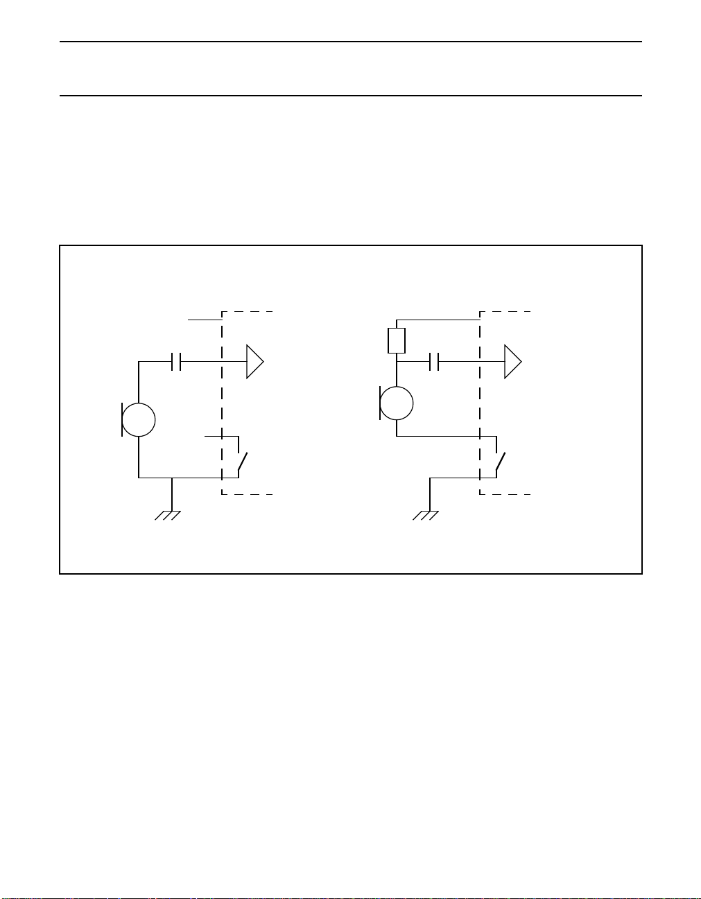
V
DDA1
17
MICP
21
MICGND
20
V
SSA1
18
PASSIVE
UCB1200 UCB1200
V
DDA1
MICGND
17
MICP
21
20
V
SSA1
18
ACTIVE
Fig.4 Possible microphone connections.
The UCB1200audio codecinput path acceptsmicrophone signalsdirectly, only aDC blocking capacitor is neededsince
the MICP input is biased around 1.4V. The ‘ground’ side of the microphone is either connected to the analog ground
)or tothe MICGNDpin. Thelatter willdecrease thecurrent consumptionof activemicrophones, sincethe MICGND
(V
ssa1
pin is made Hi-Z when the audio codec input path is disabled.
The full scale input voltage of the audio input path is programmable in 1.5 dB stepsby setting the appropriatenumber in
AUDIO_GAIN[n] in the audio control register A.
A clipdetection circuit willinform the userwhenever the inputvoltage exceeds themaximum input voltage,since this will
lead to a high distortion. In that case AUD_CLIP_STAT in the audio control register B is set. When ACLIP_RIS_INT is
set, an interrupt is generated on the IRQOUT pin on the rising edge of the clip detect signal. When ACLIP_FAL_INT is
set, an interrupt is generated on the falling edge of the clip detect signal.
The frequency responseof the audio codec depends mainly on the selected sample rate, since the bandwidth is limited
in the down and up sampling filters. These digital filters both contain several FIR and IIR low pass filters and a DC
removal filter (high passfilter). A 3rd order smoothing filter is implemented in the DAC path, between DAC andspeaker
driver stage to reduce the spurious frequencies at the speaker outputs.
1998 Jul 22 8
Philips Semiconductors Product specification
Advanced modem/audio analog front-end UCB1200
48dB
24dB
0dB
21dB
0dB
24dB
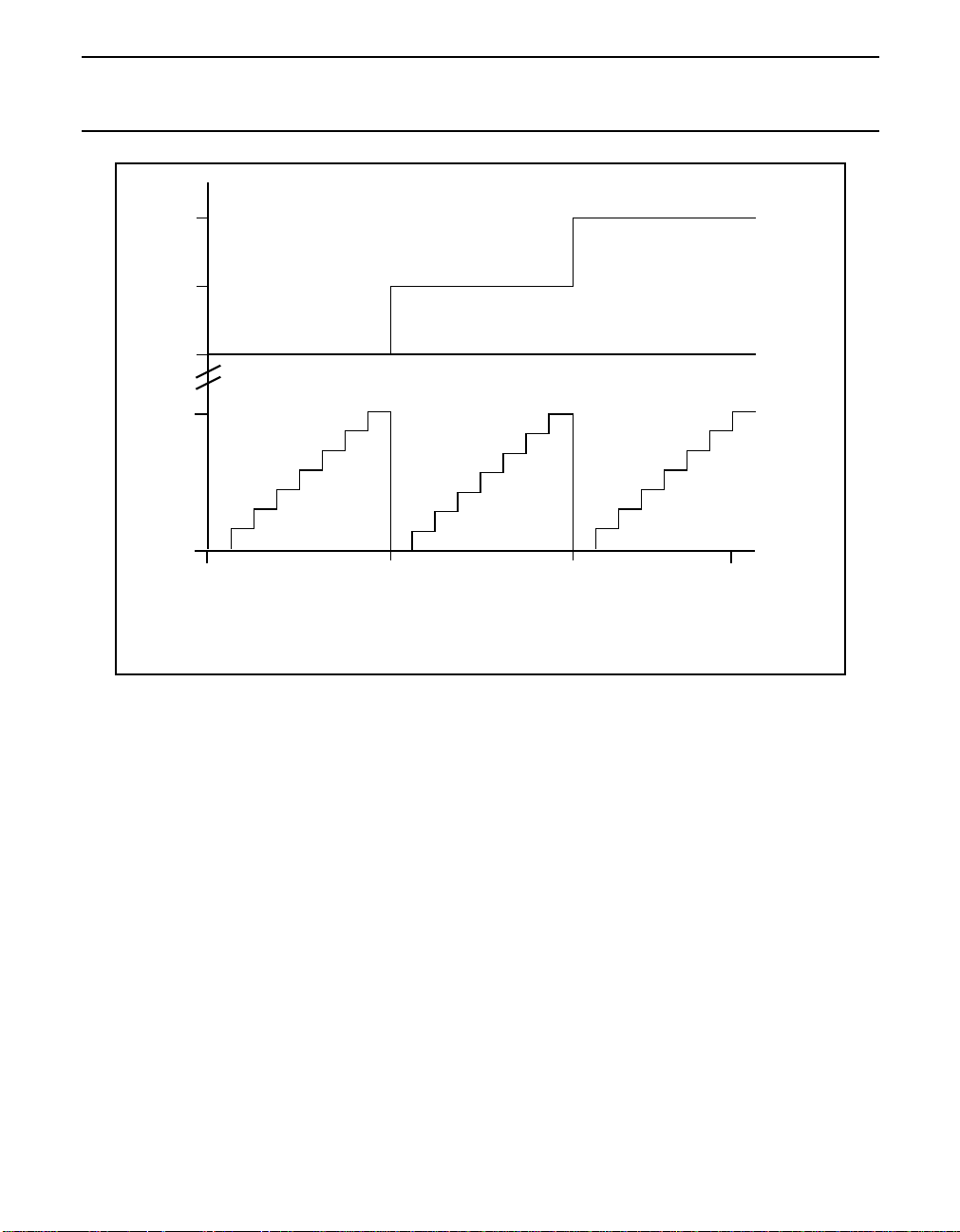
programmed attenuation
48dB 69dB
Fig.5 Analog and digital attenuation settings audio output path.
The output level can be attenuated in 3 dB steps down to -69 dB. The first 8 attenuation steps (0 to 21 dB) are
implemented in the analog domain. The digital up sample filter contains a 24 dB and a 48 dB attenuation setting. This
arrangement preservesthe resolution, thusthe ‘audio quality’ of the audio output signalfor attenuation settingstill 21 dB.
The speaker driver is muted when AUDIO_MUTE in the audio control register B is set. The speaker driver will remain
activated in that case, however no signal is produced by the speaker driver circuit.
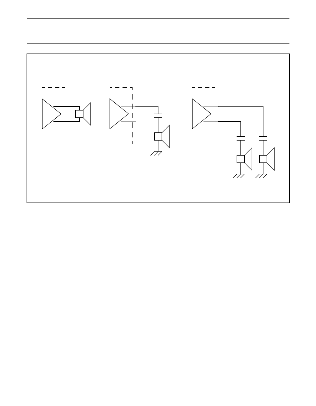
The speaker driver is designed to directly drive a bridge tied load (BTL). This yields the highest output power and this
arrangementdoes not require external DC blocking capacitors. The speakerdriver alsoaccepts singleended connection
of a speaker, in which case the maximum output power is reduced to a quarter of the BTL situation. Consequently this
way of connecting the speaker to the speaker driver reduces the power consumption of the speaker driver in the
UCB1200 by a factor of 2. Fig.6 shows possible ways to connect a speaker to the driver. Loading the amplifiers with a
capacitive load may cause high frequency oscillations and should be done cautiously.
1998 Jul 22 9
Philips Semiconductors Product specification
Advanced modem/audio analog front-end UCB1200
BRIDGE TIED
SPEAKER LOAD
UCB1200 UCB1200 UCB1200
SPKRP
9
+
8
SPKRN
SINGLE ENDED SPEAKER CONNECTIONS
SPKRP
9
8
SPKRN
SPKRP
9
8
SPKRN
+
+
Fig.6 Possible speaker connections.
The audioinput and output pathare activated independently; the input path isenabled when AUDIO_IN_ENA isset, the
output path is enabled when AUD_OUT_ENA is set in the audio control register B. This provides the user the means to
reduce the current consumption of the UCB1200 if one part of the audio codec is not used in the application.
The audio codec has a loopback mode for system test purposes, which is activated when the AUDIO_LOOP bit in the
audio control register B is set. This is an analog loopback which internally connects the output of the audio output path
to the input of the audio input path, (see Fig.3). In this mode the normal microphone input is ignored, but the speaker
driver can be operated normally.
+
1998 Jul 22 10
Philips Semiconductors Product specification
Advanced modem/audio analog front-end UCB1200
TELECOM CODEC
The telecom codec contains an input channel, built up from a 64 times oversampling sigma delta analog to digital
converter (ADC) with digital decimation filters, programmable attenuation and built-in sidetone suppression circuit.
The outputpath consist of adigital up sample filter,a 64 time oversampling 4 bit digitalto analog converter (DAC)circuit
followed bya differential outputdriver, capable ofdirectly driving a 600 Ω isolation transformer. The outputpath includes
a mute function. The telecom codec also incorporates a loopback mode, in which codec output path and the input path
are connected in series.
TOUTP
TOUTN
TINP
TINN
TEL_SIDE_ENA
SIDETONE
SUPPRESSION
CIRCUIT
TEL_MUTE
TEL_LOOP
TEL_ATT
1bit ADC
4bit DAC
DIGITAL
DECIMATION
FILTER
TEL_IN_ENA
TEL_OUT_ENA
DIGITAL
NOISE
SHAPER
14
14
Fig.7 Telecom codec block diagram.
The telecomsample rate (fst) is derived from the SIB interface clock pin (SIBCLK) and is programmable through theSIB
interface. The telecom sample rate is given by the following formula:
2F
×()
f
=
------------------------------------------------- -
st
SIBCLK
64 TEL_DIV[n]×()
(15 < TEL_DIV[n] <128)
For example, a SIBCLK of 9.216 MHz, with a divisor of 40, results in a telecom sample rate of 7.2 kHz. Both the rising
and thefalling edges of the SIBCLK are usedin case TEL_DIV[n] is set to anodd number. In that case a 50%duty cycle
of the SIBCLK signal is mandatory to obtain time equidistant sampling.
The input path of the telecom codec has a programmable attenuation. It also implements a voice band filter, which
consists of an digital low pass filter, which is a part of the decimation filter. Therefore the pass band of the voice band
1998 Jul 22 11

Philips Semiconductors Product specification
Advanced modem/audio analog front-end UCB1200
filter is determined by the selected telecom codec sample rate. This voice band filter is activated by setting
TEL_VOICE_ENA in the telecom control register B. The resulting telecom input filter curves are given in Fig.37 and
Fig.38.
The output sectionof the telecom codec is designedto interface with a 600 Ω line through an isolation transformer. The
built inmute function isactivated by TEL_MUTEin the telecomcontrol register B.The output driverremains active inthe
mute mode,however no output signalis produced. Loading thedrivers with a capacitive load may causehigh frequency
oscillations and should be done cautiously.
1998 Jul 22 12
Philips Semiconductors Product specification
Advanced modem/audio analog front-end UCB1200
TOUCH SCREEN MEASUREMENT MODES
The UCB1200 contains an on chip interface for a 4 wire resistive touch screen. This interface supports three modes of
touch screen measurements: position, pressure and plate resistance.
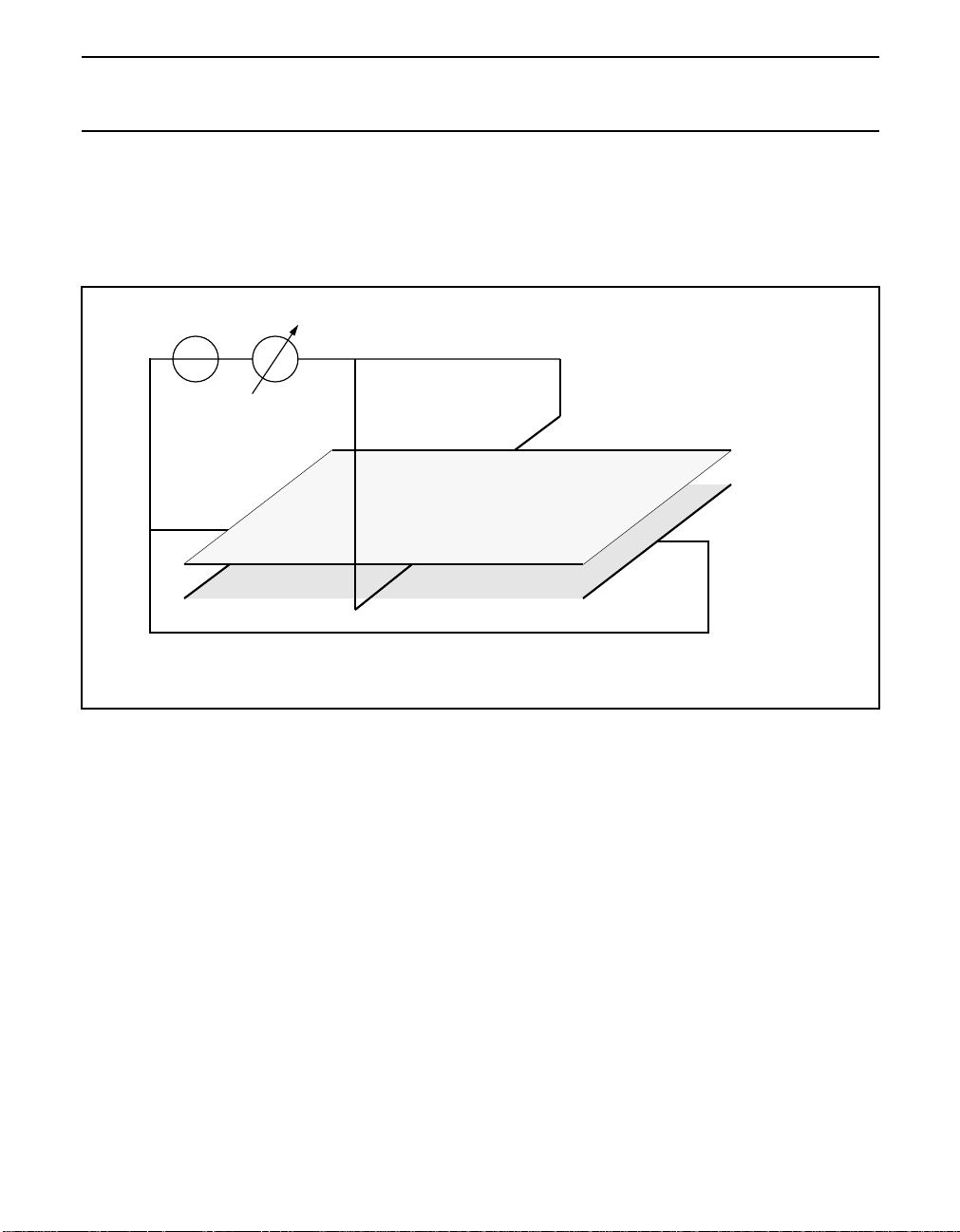
POSITION MEASUREMENT
Twoposition measurementsare neededto determinethe locationof the pressedspot. Firstan Xmeasurement, secondly
a Y measurement. TheX plate is biased duringthe Xposition measurement ofthe Xplate and thevoltage onone or both
Y terminals (TSPY, TSMY) measured. The circuit can then be represented by a potentiometer, with the TSPY and/or
TSMY electrode being the ‘wiper’. The measured voltage on the TSPY/TSMY terminal is proportional to the X position
of the pressed spot of the touch screen.
Vposition
Vtscbias
tspx
tsmy
tspy
tsmx
Fig.8 Touch screen setup for position measurement.
In the Y position mode the X plate and Y plate terminals are interchanged, thus the Y plate is biased while the voltage
on the TSPX and/or TSMX terminal is measured.
1998 Jul 22 13
Philips Semiconductors Product specification
Advanced modem/audio analog front-end UCB1200
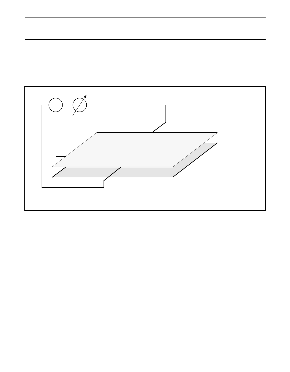
PRESSURE MEASUREMENT
Thepressure used to press the touch screen can bedetermined. Infact thecontact resistancebetween theX andY plate
is measured, which is a good indication of the size of the pressed spot and the applied pressure. A soft stylus, e.g. a
finger, leads to a rather large contact area between the two plates when a large pressure is applied. A hard stylus, e.g.
a pen, leads to less variation in measured contact resistance since the contact area is rather small.
Vtscbias
ipressure
tspx
tsmy
tspy
tsmx
Fig.9 Touch screen setup for pressure measurement.
One plate is biased at one or both terminals during this pressure measurement, whereas the other plate is grounded,
again on one or both terminals. The current flowing through the touch screen is a direct indication for the resistance
between both plates.A compensation for the series resistance, formed by the touch screenplates itself will improve the
accuracy of this measurement.
1998 Jul 22 14
Philips Semiconductors Product specification
Advanced modem/audio analog front-end UCB1200
PLATE RESISTANCE MEASUREMENT
Theplate resistanceof atouch screenvaries typicallya lotdue toprocessing spread. Knowingthe actualplate resistance
makes it possible to compensate for the plate resistance effects in pressure resistance measurements. The plate
resistance decreases when two or more spotson the touch screen are pressed. In that casea part of one plate, e.g. the
X plate is shorted by the other plate, which decreases the actual plate resistance
Vtscbias
iplate
tspx
tsmy
tspy
tsmx
Fig.10 Touch screen setup for plate resistance.
The plate resistance measurement is executed in the same way as the pressure resistance measurement. In this case
only one of the two plates isbiased and the other plate is kept floating. Thecurrent through the connected plate is again
a direct indication of the connected resistance.
1998 Jul 22 15
Philips Semiconductors Product specification
Advanced modem/audio analog front-end UCB1200
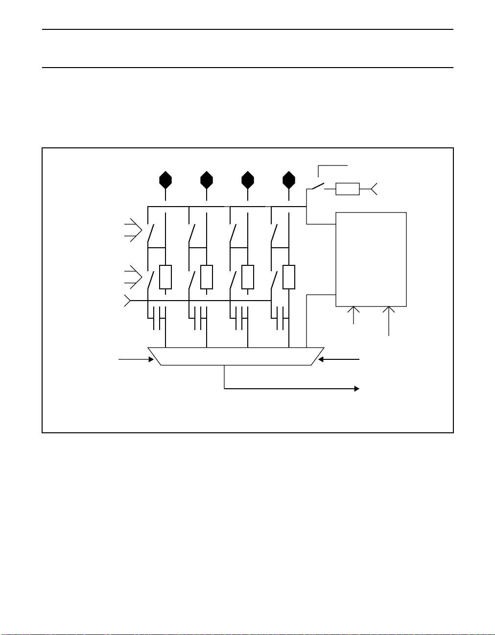
TOUCH SCREEN INTERFACE
The UCB1200 contains a universal resistive touch screen interface for 4-wire resistive touch screen, capable of
performing position, pressure and plate resistance measurements. In addition the touch screen can be programmed to
generate interrupts when the touch screen is pressed. The last mode is also active when the UCB1200 is set in the
stand-by mode.
ts..power
ts..ground
vssa3
adc_input[2:0]
tspx
tsmx
tspy
tsmy
analog mux
Fig.11 Block diagram of the touch screen interface.
tsc_mode
vdda1
touch screen
bias voltage
touch screen
current monitor
vssa1
tsc_bias_ena
tsc_mode_sel
to adc input
The touch screen interface connects to the touch screen by four wires: TSPX, TSMX, TSPY and TSMY. Each of these
pinscan beprogrammed tobe floating,powered orgrounded inthe touchscreen switchmatrix. Thesetting ofeach touch
screen pin is programmable through the touch screen control register. Possible conflicting settings (grounding and
powering ofa touch screen pinat the sametime) are detected bythe UCB1200. In that case the touchscreen pin will be
grounded.
TheUCB1200’s internalvoltage reference(V
the touch screen biasing independent of supply voltage and temperature variations. Four low pass filters, one on each
touch screen terminal, are built in to minimize the noise coupled from the LCD into the touch screen signals. An LCD
typically generateslarge noise glitcheson the touchscreen, since theyare closely coupled.The influence ofthe glitches
can neverthelessbe minimized byperforming measurements whenthe LCD isquiet. This canbe done bysynchronizing
the measurement and the video driver with the ADCSYNC pin.
1998 Jul 22 16
)is usedas referencevoltage forthe touch screenbias circuit.This makes
ref

Philips Semiconductors Product specification
Advanced modem/audio analog front-end UCB1200
Vdda
tsmy
Rint
schmitt trigger
tspx
tspy
tsmx
schmitt trigger
Fig.12 Touch screen setup for interrupt detection.
In addition to the measurements mentioned above, the touch screen can also act as an interrupt source. In this mode
the X plate of the touch screen has to be powered and the Y plate has to be grounded. In this case the touch screen is
not biased by the active touch screen bias circuit, but by a resistor to V
screen and the UCB1200 does not consume power unless the touch screen is touched. The voltage on the X plate
terminals drops if the screen is pressed. This voltage drop is detected by Schmitt-trigger circuits, of which the outputs
are connected to the interrupt control block. A touch screen interrupt is generated either when the touch screen is
pressed (fallingedge enabled) orwhen the touch screenis released (risingedge enabled). It can be used toactivate the
system around the UCB1200 to start a touch screen read-out sequence. The internal Schmitt-trigger circuits are
connected to the TSPX and TSMX signals after the built in low pass filters. This reduces the number of spurious
interrupts, due to the coupling between the LCD screen and the touch screen sensors.
Each of the four touch screen signalscan be selected as input for the built in10 bit ADC, which isused to determine the
voltage on the selected touch screen pin. The flexible switch matrix and the multi- functional touch screen bias circuit
enables the user of the UCB1200 to set each desired touch screen configuration.
The setting of the touch screen bias circuit and the ADC input multiplexer is determined by the setting of TSC_MOD[n]
in the touch screen control register according the following table.
1998 Jul 22 17
. This configuration simply biases the touch
DDA1
 Loading...