

Philips ucb1100 DATASHEETS

INTEGRATED CIRCUITS
UCB1100
Advanced modem/audio analog front-end
Preliminary specification
Supersedes data of 1996 Apr 09
Version 1.2
1998 May 08

Philips Semiconductors Preliminary specification
UCB1 100Advanced modem/audio analog front-end
Version 1.2
GENERAL DESCRIPTION
The UCB1100 is a single chip, integrated mixed signal audio and
telecom codec. The single channel audio codec is designed for
direct connection of a microphone and speaker. The built-in telecom
codec can directly be connected to a DAA and supports high speed
modem protocols. The incorporated 10 bit analogue to digital
converter and the touch screen interface provides complete control
and readout of a connected 4 wire resistive touch screen. The 10
additional general purpose I/O pins provides programmable inputs
and/or outputs to the system.
The UCB1100 has a serial interface bus (SIB) intended to
communicate to the system controller. Both the codec input and
output data and the control register data is multiplexed on this SIB
interface.
APPLICATIONS
•Personal Intelligent Communicators
•Personal Digital Assistants (PDA)
•Screen phones
•Smart Phone and smart Fax
•Intelligent Communicators
KEY FEATURES
•48-pin LQFP (SOT313-2) small body SMD package and low
external component count result in minimal PCB space
requirement.
•A 12-bit sigma delta audio codec with programmable sample rate,
input and output voltage levels, capable of connecting directly to
speaker and microphone, including digitally controlled mute,
loopback and clip detection functions
•A 14-bit sigma delta telecom codec with programmable sample
rate, including digitally controlled input voltage level, mute,
loopback and clip detection functions. The telecom codec is
intended for direct connection to a DAA (digital access
arrangement) and includes a built-in sidetone suppression circuit.
•A complete 4 wire resistive touch screen interface circuit
supporting position, pressure and plate resistance measurements.
•A 10-bit successive approximation ADC with internal track and
hold circuit and analogue multiplier for touch screen readout and
monitoring of four external high voltage (7.5V) analogue voltages.
•A high speed, 4 wire serial interface data bus (SIB) for
communication to system controller.
•A 3.3V supply voltage and built in power saving modes make the
UCB1100 optimal for portable and battery powered applications.
T ABLE OF CONTENTS
GENERAL DESCRIPTION 2. . . . . . . . . . . . . . . . . . . . . . . . . . . . . . . . .
APPLICATIONS 2. . . . . . . . . . . . . . . . . . . . . . . . . . . . . . . . . . . . . . . . . . .
KEY FEATURES 2. . . . . . . . . . . . . . . . . . . . . . . . . . . . . . . . . . . . . . . . . .
TABLE OF CONTENTS 2. . . . . . . . . . . . . . . . . . . . . . . . . . . . . . . . . . . .
1.0 FUNCTIONAL BLOCK DIAGRAM 3. . . . . . . . . . . . . . . . . . . . .
2.0 ORDERING INFORMATION 4. . . . . . . . . . . . . . . . . . . . . . . . . .
3.0 ABSOLUTE MAXIMUM RATINGS 4. . . . . . . . . . . . . . . . . . . . .
4.0 DC ELECTRICAL CHARACTERISTICS 5. . . . . . . . . . . . . . . .
5.0 PINOUT 6. . . . . . . . . . . . . . . . . . . . . . . . . . . . . . . . . . . . . . . . . . . .
5.1 PINLIST 7. . . . . . . . . . . . . . . . . . . . . . . . . . . . . . . . . . . . . .
6.0 FUNCTIONAL DESCRIPTION 8. . . . . . . . . . . . . . . . . . . . . . . .
6.1 AUDIO CODEC 8. . . . . . . . . . . . . . . . . . . . . . . . . . . . . . .
6.1.1 AUDIO INPUT SPECIFICATIONS 10. . . . . . . .
6.1.2 AUDIO OUTPUT SPECIFICATIONS 11. . . . . . .
6.2 TELECOM CODEC 12. . . . . . . . . . . . . . . . . . . . . . . . . . .
6.2.1 TELECOM INPUT SPECIFICATIONS 14. . . . .
6.2.2 TELECOM OUTPUT SPECIFICATIONS 15. . .
6.3 TOUCH SCREEN MEASUREMENT MODES 16. . . .
6.3.1 POSITION MEASUREMENT 16. . . . . . . . . . . . .
6.3.2 PRESSURE MEASUREMENT 16. . . . . . . . . . .
6.3.3 PLATE RESISTANCE MEASUREMENT 16. . .
6.4 TOUCH SCREEN INTERFACE 17. . . . . . . . . . . . . . . . .
6.4.1 TOUCH SCREEN SPECIFICATIONS 18. . . . .
6.5 10 BIT ADC. 19. . . . . . . . . . . . . . . . . . . . . . . . . . . . . . . . .
6.5.1 SPECIFICATION OVERVIEW 21. . . . . . . . . . . .
6.6 ON CHIP REFERENCE CIRCUIT 21. . . . . . . . . . . . . .
6.6.1 SPECIFICATION OVERVIEW 21. . . . . . . . . . . .
6.7 SERIAL INTERFACE BUS 22. . . . . . . . . . . . . . . . . . . . .
6.7.1 SIB DATA FORMAT 23. . . . . . . . . . . . . . . . . . . . .
6.7.2 CODEC DATA TRANSFER 24. . . . . . . . . . . . . .
6.7.3 CONTROL REGISTER DATA TRANSFER 26.
6.7.4 AC ELECTRICAL CHARACTERISTICS 27. . .
6.8 GENERAL PURPOSE I/Os 27. . . . . . . . . . . . . . . . . . . .
6.9 INTERRUPT GENERATION 27. . . . . . . . . . . . . . . . . . .
6.10 RESET CIRCUITRY 28. . . . . . . . . . . . . . . . . . . . . . . . . .
7.0 MISCELLANEOUS 29. . . . . . . . . . . . . . . . . . . . . . . . . . . . . . . . .
7.1 POWER ROUTING STRATEGY 29. . . . . . . . . . . . . . . .
8.0 CONTROL REGISTER OVERVIEW 30. . . . . . . . . . . . . . . . . .
9.0 PACKAGE OUTLINES 34. . . . . . . . . . . . . . . . . . . . . . . . . . . . . .
9.1 PACKAGE OUTLINE LQFP48 34. . . . . . . . . . . . . . . . . .
10.0 DEFINITIONS 36. . . . . . . . . . . . . . . . . . . . . . . . . . . . . . . . . . . . .
1998 May 08
2
Philips Semiconductors Preliminary specification
UCB1 100Advanced modem/audio analog front-end
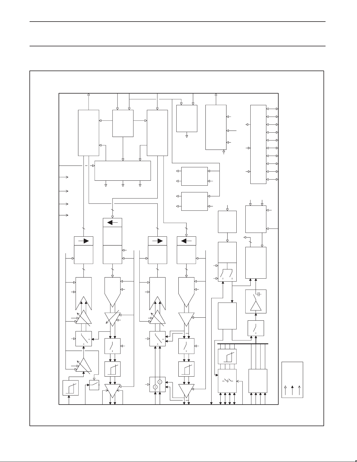
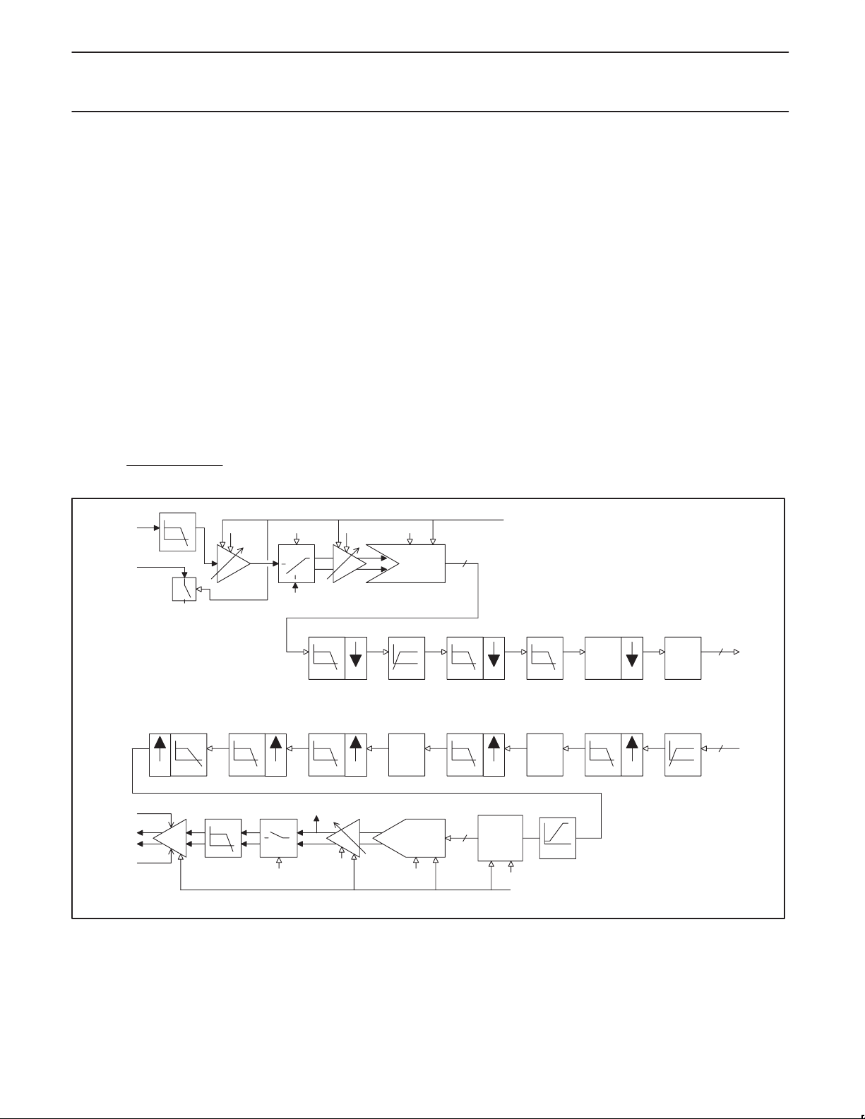
1.0 FUNCTIONAL BLOCK DIAGRAM
test
2xVddd2xVssdVdda1Vssa1
audio_input_enable
sibdout
encoder
serial bus
control data registers
to all other analog and digital blocks
fs
12
fs
12
noise
digital
filter
digital
decimation
1
64fs
digital
volume
64fs
4
sibsync
serial bus
shaper
control
sibclk
controller
serial bus
telecom input enable
audio_output_enable
attn[4,5]
sibdin
fs
14
digital
decimation
4
64fs
decoder
filter
fst 64fst
fsa 64fsa
reset
internal
fs
digital
64fs
reset
14
noise
shaper
4
nreset
stretcher
sample
frequency
sample
frequency
divider
divider
irqout
clear_interrupt[0:15]
Interrupt
controller
rising_edge_ena[0:15]
interrupt data
from other blocks
divtel0:6]
eanble data
for all
analog blocks
divaud[0:6]
power
control
telecom output enable
voltage
reference
external
filter
falling_edge_ena[0:15]
Programmable IO pin block
IOmode[0:9] IOwdat[0:9] IOrdat[0:9]
adc
start
sync
enable
stop logic
ADC start
10
to external register 11
10 bit ADC
io0 io1 io2 io3 io4 io5 io6 io7 io8 io9
adc_sync_ena
adcsync
1998 May 08
64fsa
gain[0,2]
loopback
gain[3,4]
micp
mux
1 bit ADC
micgnd
4 bit DAC
AUDIO CODEC
attn[0,3]
vssa1
spkrp
spkrn
vdda2
vssa2
external
reference
64fsa
effect
mute
echo on loopback
side tone suppression
1 bit ADC
attenuation
mux
tinp
TELECOM CODEC
tinn
4 bit DAC
toutp
toutn
effect
mute
vrefbyp
Figure 1. Block Diagram of the UCB1100
3
bias voltage
touch screen
touch screen
switch matrix
tspy
tsmx
tsmy
vssa3
mux
switched
ad0
ad1
track & hold
9 to 1
voltage
dividers
ad2
ad3
analog pin
digital pin
SN00126
supply pin
Philips Semiconductors Preliminary specification
Á
Á
Á
Á
Á
Á
UCB1 100Advanced modem/audio analog front-end
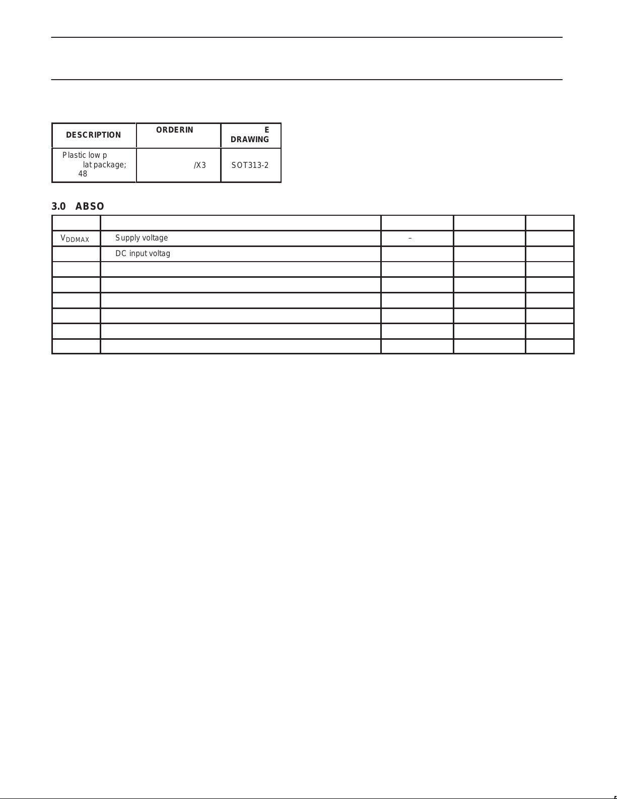
2.0 ORDERING INFORMATION
DESCRIPTION
ÁÁÁÁ
ORDERING
БББББ
CODE
Plastic low profile
quad flat package;
ÁÁÁÁ
48 leads
UCB1100LP/X3
БББББ
3.0 ABSOLUTE MAXIMUM RATINGS
SYMBOL PARAMETER MIN MAX UNIT
V
DDMAX
V
IMAX
V
ADMAX
V
OMAX
I
IKMAX
I
OKMAX
I
OLMAX
T
stg
NOTES:
1. Stresses above those listed under Absolute Maximum Ratings may cause permanent damage to the device. This is a stress rating only and
functional operation of the device at these or any conditions other than those described in the Absolute Maximum Rating section of this
specification is not implied.
2. This product includes circuitry specially designed for the protection of its internal devices from damaging ef fects of excessive static charge.
Nonetheless, it is suggested that conventional precautions be taken to avoid submitting the UCB1100 to conditions exceeding the maximum
ratings.
3. Parameters are valid over the operating ambient temperature unless otherwise specified. All voltages are with respect to the V
unless otherwise noted.
Supply voltage –0.5 5.0 V
DC input voltage, except AD0–3 inputs –0.5 VDD+0.5 V
DC input voltage AD0–3 inputs –0.5 8.5 V
DC output voltage –0.5 VDD+0.5 V
DC diode input current, all inputs 10 mA
DC diode output current 10 mA
Continuous output current, digital outputs 4 mA
Storage temperature –55 150 °C
PACKAGE
ÁÁÁ
DRAWING
SOT313-2
ÁÁÁ
SSD
pin,
1998 May 08
4
Philips Semiconductors Preliminary specification
SYMBOL
PARAMETER
NOTES
UNIT
UCB1 100Advanced modem/audio analog front-end
4.0 DC ELECTRICAL CHARACTERISTICS
T
= 0°C to 70°C, V
amb
Voltage with respect to the V
V
DDD
V
DDA1
V
DDA2
V
SSA2
V
SSA3
I
DDD
I
DDA1
I
DDA2
V
TSCB
I
TSCB
V
ADFS
V
TSFS
V
IL
V
IH
V
OL
V
OH
f
SIBCLK
T
amb
NOTES:
1. Indicative value only. Value will be frozen following silicon measurements.
2. Excluding connected touch screen and speaker load currents.
SSD
= V
= V
SSA1
pin, unless otherwise specified.
SSD
SSA2
= V
= 0V , sibclk = 10MHz, audio_divisor = 12, telecom_divisor = 40.
SSA3
LIMITS
MIN TYP MAX
digital supply voltage 3.0 3.3 3.6 V
analogue supply voltage (excl.speaker driver) 3.0 3.3 3.6 V
analogue supply voltage (speaker driver only) 3.0 3.3 3.6 V
analogue ground voltage wrt. V
analogue ground voltage wrt V
digital supply current,
SSD
SSD
Note 1
–0.4 0 0.4 V
–0.4 0 0.4 V
full functionality 19 mA
only audio codec activated 17 mA
only telecom codec activated 19 mA
only touch screen activated 15 mA
only adc activated 15 mA
no functions activated, sibclk stopped 10 µA
analogue supply current,
Note 1, Note 2
full functionality 3.8 mA
only audio codec activated 1.5 mA
only telecom codec activated 1.7 mA
only touch screen activated 0.4 mA
only adc activated 0.5 mA
no analogue functions activated <10 µA
total speaker driver supply current
Note 1, Note 2
full functionality 0.2 mA
only audio codec activated 0.2 mA
only telecom codec activated 10 µA
only touch screen activated 10 µA
only adc activated 10 µA
no analogue functions activated 10 µA
touch screen bias voltage 1.8 V
maximum touch screen bias current 10 mA
full scale voltage ad0–ad3 inputs 7.5 V
full scale input touch screen inputs 7.5 V
input low voltage –0.5 0.3*V
input high voltage 0.7*V
DDD
V
DDD
output low voltage IOL=2mA 0.2*V
output high voltage IOH=2mA 0.8*V
DDD
DDD
+0.5 V
DDD
V
V
V
clock frequency 0 10 15 MHz
Operating Ambient Temperature 0 70 °C
1998 May 08
5
Philips Semiconductors Preliminary specification
UCB1 100Advanced modem/audio analog front-end
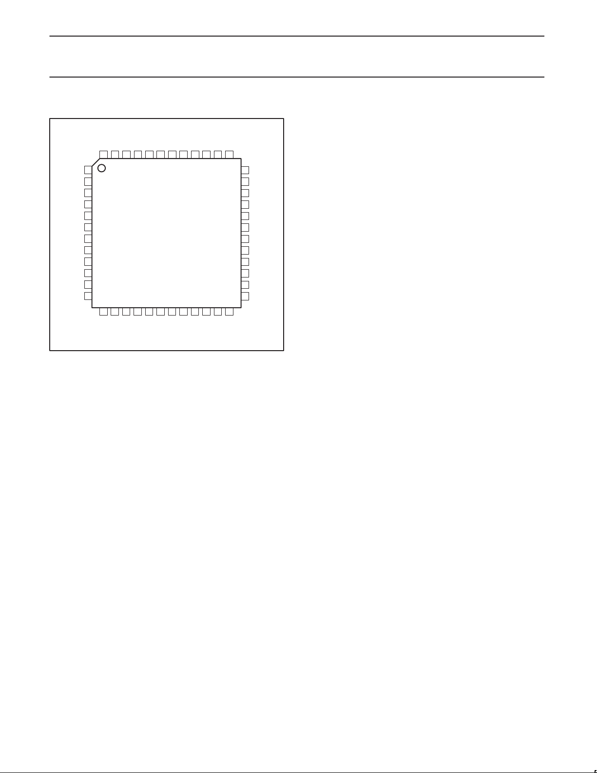
5.0 PINOUT
vddd
io6
io5
io4
not used
irqout
sibdin
sibclk
sibdout
sibsync
nreset
vssd
adcsync
vssd
not used
vssa2
spkrn
sprkp
vdda2
toutp
toutn
io7
io8
io9
4847464544434241403938
1
2
3
4
5
6
7
8
9
10
11
12
UCB1100
LQFP48
TOP VIEW
37
36
io3
35
io2
34
io1
33
io0
32
vddd
31
not used
30
tspx
29
tsmy
28
tsmx
27
tspy
26
vssa3
25
ad0
1314151617181920212223
test
tinn
tinp
vrefbyp
vdda1
vssa1
not used
micgnd
micp
ad3
Figure 2. LQFP48 (SOT313-2)
ad2
24
ad1
SN00127
1998 May 08
6

Philips Semiconductors Preliminary specification
SYMBOL
PIN TYPE
DESCRIPTION
NOTE
UCB1 100Advanced modem/audio analog front-end
5.1 Pinlist
PINNING
LQFP48
vddd 32, 48 supply digital supply
vssd 5, 37 ground digital ground 1
vdda1 17 supply analogue supply
vssa1 18 ground analogue ground 1
vdda2 10 supply analogue speaker driver supply
vssa2 7 ground analogue speaker driver ground
vssa3 26 ground touch screen switch matrix ground
sibclk 41 CMOS input SIB serial interface master clock
sibdin 42 CMOS input SIB data input
sibdout 40 CMOS output ‘0’ / Hi-Z SIB data output 2
sibsync 39 CMOS input SIB synchronization
irqout 43 CMOS output
micp 21 analogue input Hi-Z microphone signal input
micgnd 20 analogue input Hi-Z microphone ground switch input
sprkp 9 analogue output Hi-Z positive speaker output 3
spkrn 8 analogue output Hi-Z negative speaker output 3
tinp 15 analogue input Hi-Z positive telecom codec input 3
tinn 14 analogue input Hi-Z negative telecom codec input 3
toutp 11 analogue output Hi-Z positive telecom codec output 3
toutn 12 analogue output Hi-Z negative telecom codec output 3
ad0–3 25–22 analogue input Hi-Z analogue high voltage inputs
tspx 30 analogue IO Hi-Z positive X-plate touch screen
tsmx 28 analogue IO Hi-Z negative X-plate touch screen
tspy 27 analogue IO Hi-Z positive Y-plate touch screen
tsmy 29 analogue IO Hi-Z negative Y-plate touch screen
adcsync 4 digital input adc synchronization pulse input
vrefbyp 16 analogue IO Hi-Z external reference voltage input, external filter connection
io0–9 33–36,
45–47,
1–3
nreset 38 CMOS input
test 13 CMOS input ‘0’ test mode protection 4
not used 6, 19,
31, 44
NOTES:
1. The vssd and vssa1 pins are connected to each other within the UCB1100.
2. The first 64 bits of the sib frame will be ‘0’, the remaining bits in the sib frame will be Hi-Z.
3. The spkrp/spkrn, tinp/tiln and toup/toutn are dif ferential pairs.
4. The test pin contains a internal pull down. This pin should be connected to vssd in normal mode of the UCB1100.
active-High
CMOS IO input general purpose IO pins
active-Low
RESET
STATE
‘0’ interrupt output
asynchronous reset input
not connected pins
1998 May 08
7
Philips Semiconductors Preliminary specification
UCB1 100Advanced modem/audio analog front-end
6.0 FUNCTIONAL DESCRIPTION
The UCB1100 consists of several analogue and digital sub circuits
which can be programmed via the Serial Interface Bus (SIB). This
enables the user to set the UCB1100 functionality according actual
application requirements.
6.1 Audio codec
The audio codec contains an input channel, built up from a 64 times
oversampling sigma delta analogue to digital converter (ADC) with
digital decimation filters and a programmable gain microphone
preamp. The output path consists of a digital up sample filter, a 64
time oversampling 4 bit digital to analogue converter (DAC) circuit
followed by a speaker driver, capable of driving directly a low
impedance bridge tied (BTL) speaker. The output path features
digitally programmable attenuation and a mute function. The audio
codec also incorporates a loopback mode, in which codec output
path and the input path are connected in series.
The audio sample rate is derived from the SIB interface clock pin
(SIBclk) and is programmable through the SIB interface. The audio
sample rate is given by the following equation:
(2 *
Fsibclk
Fsa
micp
micgnd
audio_divisor
(64 *
)
(5
)
gain[3,4]
audio_divisor
loopback
mux
128)
gain[0,2]
64fsa
1 bit ADC
For example, a serial clock of 10 MHz, with a divisor of 14, results in
an audio sample rate of 22.321kHz. Both the rising and the falling
edges of the sibclk are used in case an odd audio_divisor is set.
Thus a 50% duty cycle of the sibclk signal is mandatory to obtain
time equidistant sampling with odd divisors.
The frequency response of the audio codec depends mainly on the
selected sample rate, since the bandwidth is limited in the down and
up sampling filters. These digital filters both contain several FIR and
IIR low pass filters and a DC removal filter (high pass filter). A 1st
order analogue anti aliasing filter is implemented at the input of the
microphone input to prevent aliasing in the adc path. A 3rd order
smoothing filter is implemented between dac and speaker driver
stage to reduce the spurious frequencies at the speaker outputs.
The audio codec input (=ADC) and output (= DAC) paths can be
enabled individually by setting the audio_adc and/or audio_dac bits
in the audio control register B. These enable bits operate both on
the associated analogue and digital functions, for optimal power
control of both the analogue and the digital parts.
audio_input_enable
64fs
1
vdda2
spkrp
spkrn
vssa2
vssa1
interpolator
4
low pass
FIR
loop input
16
2
mute
Sinc4
FIR
half band
FIR
loop input
attn[0,3]
2
DC
removal
round
up
4 bit DAC
64fsa
half band
WDF
half band
WDF
64fs
4
Figure 3. Detailed Block Diagram Audio codec
2
2
digital
volume
control
attn[4,5]
audio_output_enable
half band
WDF
+3dB
noise
shaper
+3dB
round
2
DC
removal
2
fs
12
up
fs
12
SN00128
1998 May 08
8

Philips Semiconductors Preliminary specification
UCB1 100Advanced modem/audio analog front-end
UCB1100 UCB1100
vdda1
micp
micgnd
vssa1
vdda1
micp
micgnd
vssa1
‘Passive’ Microphone ‘Active’ Microphone
SN00129
Figure 4. Possible Microphone Connections
The UCB1100 audio codec input path accepts microphone signals
directly, only a DC blocking capacitor is needed, since the micp input
is biased around 1.4V . The ‘ground’ side of the microphone is either
connected to the analogue ground (vssa1) or to the micgnd pin of
the UCB1100. The latter will decrease the current consumption of
active microphones, since the micgnd pin is made Hi-Z when the
audio codec input path is disabled.
The full scale input voltage of the audio input path is programmable
in 1.5dB steps by setting the appropriate data in the
audio-input-gain
bits in the audio control register A.
A clip detection circuit will inform the user whenever the input
voltage exceeds the maximum input voltage. In that case the
detect status
bit in audio control register B is set. An interrupt is
generated on the irqout pin of the UCB1100 whenever the
clip detect rising interrupt
audio
edge interrupt
bit is set in the rising edge interrupt enable or falling
or the
enable audio detect falling
clip
enable
edge interrupt control register B is set.
48dB
24dB
digital attenuation
0dB
21dB
analog attenuation
0dB
24dB 48dB 69dB
programmed attenuation
SN00130
Figure 5. Analogue and Digital Attenuation Settings
Audio Output Path
The output level can be attenuated in 3dB steps down to -69dB. The
8 highest attenuation steps are implemented in the analogue
circuitry, while the two 24dB steps are implemented in the digital
domain. This preserves the ‘audio quality’ of the output signal at
lowest attenuation settings. The speaker driver is muted when the
audio-mute
bit in the audio control register B is set. The speaker
driver will remain activated in that case, however no signal is
produced by the speaker driver circuitry.
UCB1100 UCB1100 UCB1100
spkrp
spkrn
Bridge Tied
spkrp spkrp
spkrn spkrn
Single Ended Speaker Connections
Speaker
Load
SN00131
Figure 6. Possible Speaker Connections
The speaker driver is designed to directly drive a bridge tied load
(BTL). This yields the highest output power and it does not require
external DC blocking capacitors. The speaker driver also accepts
single ended connection of a speaker, in which case the maximum
output power is reduced to a quarter of the BTL situation.
Consequently this way of connecting the speaker to the speaker
driver reduces the power consumption of the speaker driver in the
UCB1100 by a factor of 2. Figure 6 shows possible ways to connect
a speaker to the UCB1100.
The audio input and output path are activated independently; the
input path is enabled when the
output path is enabled when the
audio-input-enable
audio-output-enable
bit is set, the
bit is set in the
audio control register B. This provides the user the means to reduce
the current consumption of the UCB1100 if one part of the audio
codec is not used in the application.
The audio codec has a loopback mode for system test purposes,
which is activated when the
audio_loopback enable
bit in the audio
control register B is set. This is an analogue loopback which
internally connects the output of the audio output path to the input of
the audio input path, (see Figure 3). In this mode the normal
microphone input is ignored, but the speaker driver can be operated
normally .
1998 May 08
9

Philips Semiconductors Preliminary specification
SYMBOL
PARAMETER
CONDITIONS
UNIT
UCB1 100Advanced modem/audio analog front-end
6.1.1 Audio Input Specifications
LIMITS
MIN TYP MAX
F
SA
V
INAM
V
MICP
R
INPAI
R
HINE
G
SA
N
AGS
G
mA
G
EAR
ROES
AI
DNA
AI
THUD
AI
THD
MGAI
SNR
AI
SNR
MGAI
RIP
IA
SBR
IA
E
IA
NOTE: Coding scheme for ADC output data is 2’s complement.
audio sample frequency 26 kHz
full scale input voltage 0 dB gain setting 0.28 V
pp
DC bias voltage micp input audio input path enabled 1.4 V
input impedance audio input path enabled 25 kΩ
impedance micgnd to vssa1 audio input path enabled 100 Ω
gain step size 1.3 1.5 1.7 dB
number of gain steps 32
maximum gain 46.5 dB
gain error (accuracy of gain setting)
0 dB gain setting,
full scale input voltage
–1 0 1 dB
resolution audio input 12 bit
differential non linearity audio input ADC 0.9 LSB
total harmonic distortion
total harmonic distortion
signal to noise ratio
audio input
signal to noise ratio
pass band ripple F
stop band rejection
audio input
out of band rejection
audio input
0db input gain selected
0.28Vpp, 1kHz to micp
46.5dB gain setting,
1mVpp, 1kHz to micp
0dB input gain selected
0.28Vpp, 1kHz to micp
46.5dB gain selected
1mVpp, 1kHz to micp
<Fsig < F
PLAI
F
<Fsig.<20kHz 70 dB
SHAI
PHAI
65 dB
50 dB
0.03 %
0.1 %
0.5 dB
F > 20kHz t.b.f. mVrms
RIP
IA
0dB
SBR
IA
F
PLA
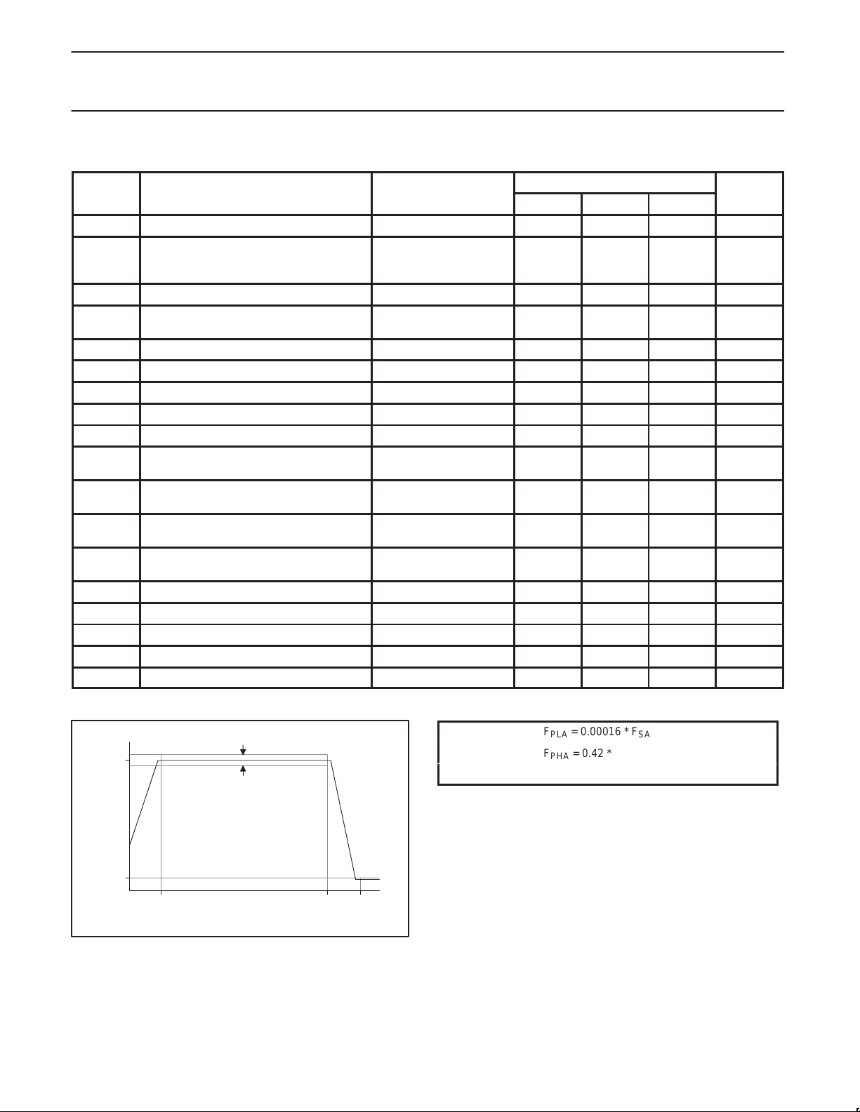
FREQUENCY (Hz)
Figure 7. Audio Input Path Frequency Response
1998 May 08
F
= 0.00016 * F
PLA
F
= 0.42 * F
PHA
F
= 0.6 * F
SHA
F
F
SHA
PHA
SN00132
SA
SA
SA
10
Philips Semiconductors Preliminary specification
SYMBOL
PARAMETER
CONDITIONS
UNIT
UCB1 100Advanced modem/audio analog front-end
6.1.2 Audio Output Specifications
LIMITS
MIN TYP MAX
V
OFFIA
V
OOA
V
OFFOA
V
SPK
A
SOA
NSOA number of attenuation steps 24
A
MOA
ROES
OA
DNA
OA
THUD
OAS
THUD
OAH
SNR
OAS
SNR
OAH
RIP
OA
F
SUOA
SBR
OA
E
IOA
Z
SPKR
NOTE: Coding scheme for DAC input data is 2’s complement.
offset error No signal applied to micp 0 LSB
0dB attenuation,
full scale output voltage
offset error 16ohm speaker 50 mV
DC bias voltage
spkrp and spkrn pin
16ohm speaker
3.2 V
differential Spkrp–Spkrn
Audio output path enabled 1.4 V
pp
pp
attenuation step size 2.8 3.0 3.2 dB
maximum attenuation 69 dB
resolution 12 bit
differential non linearity DAC 0.9 LSB
total harmonic distortion
16Ω speaker
total harmonic distortion
1kΩ headphone
signal to noise ratio
16Ω speaker
signal to noise ratio,
1kHΩ headphone
pass band ripple F
cut off frequency upper stop band 0.6 F
stop band rejection F
0dB attenuation
20Hz to 20kHz
0dB attenuation
20Hz to 20kHz bandwidth
0dB attenuation
20Hz to 20kHz bandwidth
0dB attenuation
20Hz to 20kHz bandwidth
< Fsig <– F
PLAO
<Fsig.<20kHz 70 dB
SHAO
PHAO
0.5 2 %
0.03 %
40 80 dB
65 80 dB
0.5 dB
SA
integrated out of band energy F > 20kHz 30 mVrms
speaker impedance 8 16 Ω
RIP
OA
0dB
SBR
OA
F
PLA
FREQUENCY (Hz)
Figure 8. Audio Output Filter Frequency Response
1998 May 08
F
PHA
F
SHA
SN00133
F
= 0.00016 * F
F
F
PLA
PHA
SHA
= 0.42 * F
= 0.6 * F
SA
SA
SA
11
 Loading...