

Philips uc3842 DATASHEETS
Philips Semiconductors Linear Products Product specification
UC3842Current-mode PWM controller
1100
August 31, 1994 853-0614 13721
DESCRIPTION
The UC3842 is available in an 8-Pin mini-DIP the necessary
features to implement off-line, fixed-frequency current-mode control
schemes with a minimal external parts count. This technique results
in improved line regulation, enhanced load response characteristics,
and a simpler, easier to design control loop. Topological advantages
include inherent pulse-by-pulse current limiting.
Protection circuitry includes built-in undervoltage lock-out and
current limiting. Other features include fully-latched operation, a 1%
trimmed bandgap reference, and start-up current less than 1mA.
These devices feature a totem-pole output designed to source and
sink high peak current from a capacitive load, such as the gate of a
power MOSFET. Consistent with N-channel power devices, the
output is low in the OFF-state.
FEATURES
•Low start-up current (≤1mA)
•Automatic feed-forward compensation
•Pulse-by-pulse current limiting
•Enhanced load response characteristics
•Undervoltage lock-out with hysteresis
•Double pulse suppression
•High current totem-pole output
•Internally-trimmed bandgap reference
•400kHz operation, guaranteed min
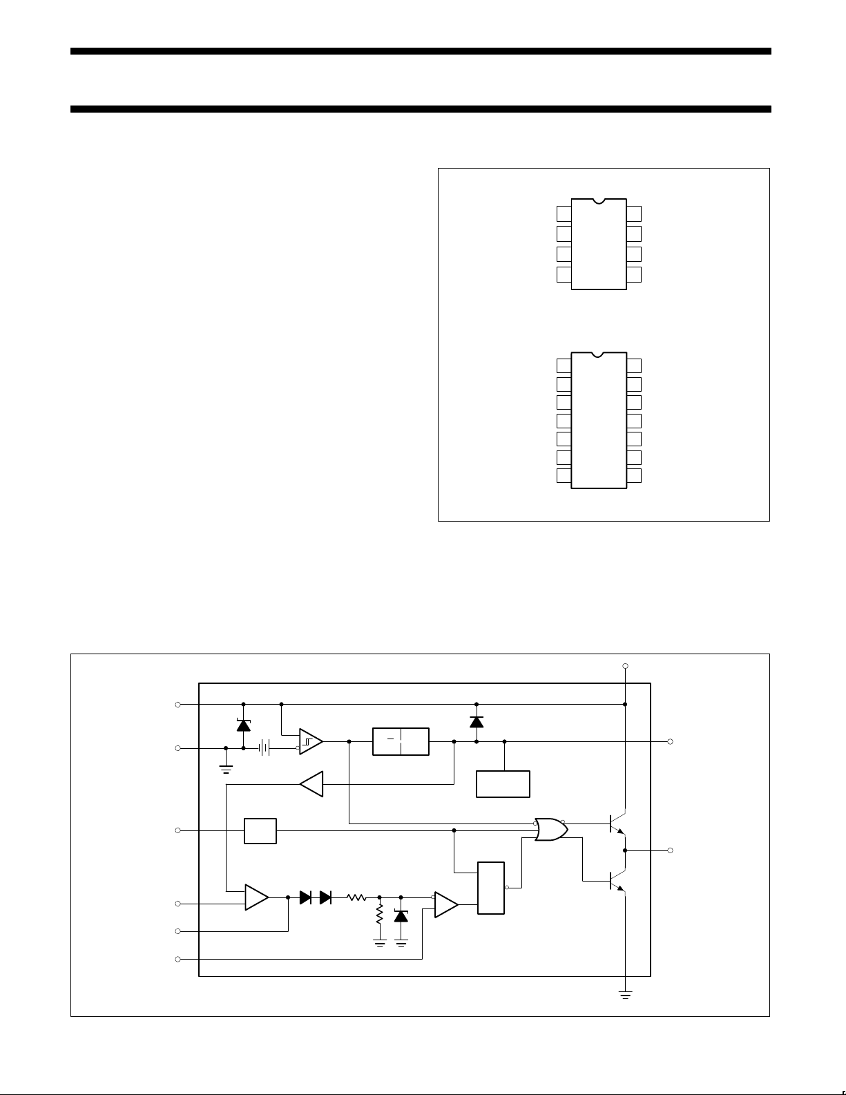
PIN CONFIGURATIONS
N Package
D Package
1
2
3
4 5
6
7
8
1
2
3
4
5
6
7 8
14
13
12
11
10
9
COMP
NC
COMP
V
FB
I
SENSE
RT/C
T
V
FB
I
SENSE
RT/C
T
NC
NC
V
REF
V
CC
OUTPUT
GROUND
NC
V
REF
V
CC
OUTPUT
GROUND
V
C
POWER GROUND
TOP VIEW
TOP VIEW
APPLICATIONS
•Off-line switched mode power supplies
•DC-to-DC converters UC3842
BLOCK DIAGRAM
NOTE:
Pin numbers in parentheses refer to the D package.
(12)7
(9)5
(7)4
(3)2
(1)1
(5)3
7(11)
8(14)
6(10)
5(8)
GND
COMP
CURRENT
SENSE
CURRENT
SENSE
COMPARATOR
PWM
LATCH
INTERNAL
BIAS
5V
REF
UVLO
34V
16V
OSC
ERROR
AMP
+
–
2R
R
1V
2.5V
5.0V
50mA
OUTPUT
6V
V
REF
V
CC
V
FB
S/R
RT/C
T
S
R
Philips Semiconductors Linear Products Product specification
UC3842Current-mode PWM controller
August 31, 1994
1101
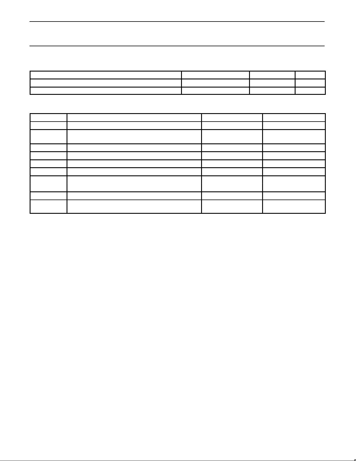
ORDERING INFORMATION
DESCRIPTION TEMPERATURE RANGE ORDER CODE DWG #
8-Pin Plastic Dual In-Line Package (DIP) 0 to +70°C UC3842N 0404B
14-Pin Plastic Small Outline (SO) Package 0 to +70°C UC3842D 0405B
ABSOLUTE MAXIMUM RATINGS
1
SYMBOL
PARAMETER RATING UNIT
V
CC
Supply voltage (ICC<30mA) Self-Limiting
V
CC
Supply voltage
(low impedance source)
30 V
I
OUT
Output current
2, 3
±1 A
Output energy (capacitive load) 5 µJ
Analog inputs (Pin 2, Pin 3) -0.3 to 6.3 V
Error amp output sink current 10 mA
P
D
Power dissipation at TA≤70°C 1 W
(derate 12.5mW/°C for TA>70°C)
2
T
STG
Storage temperature range -65 to +150 °C
T
SOLD
Lead temperature
(soldering, 10sec max)
300 °C
NOTES:
1. All voltages are with respect to Pin 5; all currents are positive into the specified terminal.
2. See section in application note on “Power Dissipation Calculation”.
3. This parameter is guaranteed, but not 100% tested in production.
Philips Semiconductors Linear Products Product specification
UC3842Current-mode PWM controller
August 31, 1994
1102
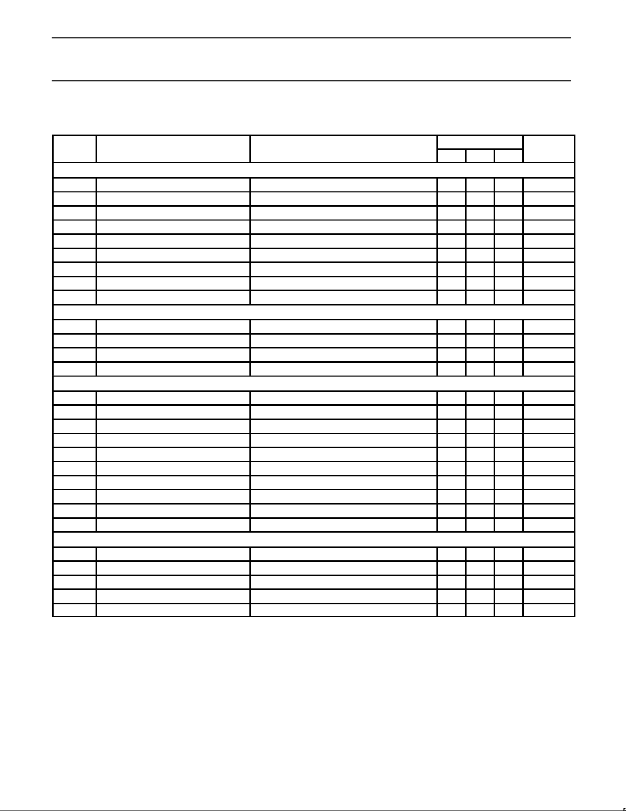
DC AND AC ELECTRICAL CHARACTERISTICS
0≤TJ≤70°C for UC3842; VCC=15V; RT=10kW; CT=3.3nF, unless otherwise specified.
UC3842
SYMBOL
PARAMETER
TEST CONDITIONS
Min Typ Max
UNIT
Reference section
V
OUT
Output voltage TJ=25°C, IO=1mA 4.90 5.00 5.10 V
Line regulation 12≤VIN≤25V 6 20 mV
Load regulation 1≤IO≤20mA 6 25 mV
Temp. stability
1
0.2 0.4 mV/°C
Total output variation
1
Line, load, temp. 4.82 5.18 V
V
NOISE
Output noise voltage
1
10Hz≤f≤10kHz, TJ=25°C 50 µV
Long-term stability
1
TJ=125°C, 1000 Hrs. 5 25 mV
Output short-circuit TJ=25 -30 -100 -130 mA
Output short-circuit -55<TJ≤0°C -30 -100 -180 mA
Oscillator section
Initial accuracy TJ=25°C 47 52 57 kHz
Voltage stability 12≤VCC≤25V 0.2 1 %
Temp. stability
1
T
MIN≤TJ≤TMAX
5 %
Amplitude V
PIN 4
peak-to-peak 1.7 V
Error amp section
Input voltage V Pin 1=2.5V 2.42 2.50 2.58 V
I
BIAS
Input bias current -0.3 -2 µA
A
VOL
2≤VO≤4V 65 90 dB
Unity gain bandwidth
1
TJ=25°C 0.7 1 MHz
Unity gain bandwidth T
MIN<TJ<TMAX
0.5 MHz
PSRR Power supply rejection ratio 12≤VCC≤25V 60 70 dB
I
SINK
Output sink current V
PIN 2
=2.7V, V
PIN 1
=1.1V 2 6 mA
I
SOURCE
Output source current V
PIN 2
=2.3V, V
PIN 1
=5V -0.5 -0.8 mA
V
OUT
High V
PIN 2
=2.3V, RL=15k to ground 5 6 V
V
OUT
Low V
PIN 2
=2.7V, RL=15k to Pin 8 0.7 1.1 V
Current sense section
Gain
2, 3
2.85 3 3.15 V/V
Maximum input signal
2
V
PIN 1
=5V 0.9 1 1.1 V
PSRR Power supply rejection ratio
2
12≤VCC≤25V 70 dB
I
BIAS
Input bias current -2 -10 µA
Delay to output
1
150 300 ns
 Loading...