

Philips uba2050x, uba2051x DATASHEETS

INTEGRATED CIRCUITS
DATA SH EET
UBA2050(A); UBA2051(A;C)
One-chip telephone ICs with
speech, dialler and ringer functions
Product specification
Supersedes data of 1998 Mar 24
File under Integrated Circuits, IC03
2000 May 19

Philips Semiconductors Product specification
One-chip telephone ICs with speech,
dialler and ringer functions
FEATURES
Speech/transmission part
• Low DC line voltage; operates down to 1.45 V
(excluding voltage drop over external polarity guard)
• Line voltage regulator with adjustable DC voltage
• Regulated 3.3 V supply (VDD) for the dialler part and
peripherals compatible with:
– Speech mode
– Ringer mode
– Trickle mode.
• Unregulated supply (VCC) for the transmission part and
peripherals
• Transmit stage with:
– Microphone amplifier with symmetrical
high-impedance inputs
– DTMF input with confidence tone on receive output.
• Receive stage with:
– Receive amplifier with asymmetrical output
– Earpiece amplifier with adjustable gain (and gain
boost facility) for all types of earpieces.
• AGC: line loss compensation for microphone and
receive amplifiers.
Dialler part
• Last Number Redial (LNR) (32 digits)
• Pulse dialling:
– 10 PPS and 20 PPS (resistor option)
– M/B 2 : 3 and 1 : 2 (resistor option).
• DTMF timing:
– Manual diallingwith minimum duration for bursts and
pauses (85/85 ms)
– Calibrated timing during redialling (85/85 ms).
• Pulse or tone mode select at start-up (resistor option)
• Flash function (600, 300, 98 and 80 ms) (resistor
options)
• Access pause time 2.0 and 3.6 s (resistor option);
access pauses in series are possible
UBA2050(A); UBA2051(A;C)
•[∗/T] key (for mixed mode dialling) or separate
[P → T] key
• Repertory memory integrity check
• Keytone generation (only UBA2050, UBA2050A and
UBA2051C)
• Dial Mode Output (DMO) function during pulse dialling
and flash function (only UBA2050 and UBA2051)
• LED output for DTMF dialling indication (only
UBA2050A and UBA2051A)
• Function keys:
– [LNR/P], [R] and [P → T]
– [STORE], [MEM], [M1], [M2] and [M3]
(only UBA2051, UBA2051A and UBA2051C).
• Resistor options:
– [∗/T] key definition (MMS)
– Pulse or Tone mode Selection (PTS)
– Flash Time Selection (FTSA and FTSB)
– Make/Break ratio Selection (MBS)
– Pulses Per Second (PPS)
– Access Pause Time (APT).
• 13 repertory numbers (only UBA2051, UBA2051A and
UBA2051C):
– 3 direct memories (21 digits)
– 10 indirect memories (21 digits).
• Supply and temperature independent tone output
• On-chip DTMF filtering for low output distortion
(
“CEPT CS 203”
• On-chip oscillator suitable for low-cost 3.579545 MHz
quartz crystal or ceramic resonator
• Uses standard single-contact keyboard
• Keyboard entries fully debounced.
Ringer part
• Ringer input frequency discrimination
• 3-toneringer with 4 programmable melodies (selectable
via keyboard by keys [1] to [4])
• 4-level volume control (selectable via keyboard by
keys [5] to [8]).
compatible)
2000 May 19 2
Philips Semiconductors Product specification
One-chip telephone ICs with speech,
dialler and ringer functions
GENERAL DESCRIPTION
TheICs UBA2050,UBA2050A,UBA2051,UBA2051Aand
UBA2051C contain all the functionsneeded to build a fully
electronic telephone set.
In many places in the text, figures and tables, the
description is not applicable for all the five types, but only
for one or two or for a combination. These combinations
will be referred to by means of short denotations as given
in Table 1.
Table 1 Denotations of types
DENOTATION TYPES
UBA2050x UBA2050; UBA2050A
UBA2051x UBA2051; UBA2051A; UBA2051C
UBA205x UBA2050; UBA2051
UBA205xA UBA2050A; UBA2051A
UBA205xx all five types
UBA2050(A); UBA2051(A;C)
When the line current is high enough, a fixed amount of
current is derived from pin LN in order to create a supply
point at pin V
3.3 V to supply the dialler and ringer parts and peripheral
circuits.
Dialler part
The dialler and ringer parts of the IC are responsible for
the system control, system settings and the generation
and detection of various signals.
The dialler offers a 32-digit last number redial function.
The UBA2051x offers in addition 13 memories
(3 direct + 10 indirect) of 21 digits.
During pulse dialling the DMO output of the UBA205x can
be used to decrease the line voltage. During tone dialling
theLED output ofthe UBA205xA is usedto indicate DTMF
dialling. A keytone is available if a valid key is pressed for
the types UBA2050x and UBA2051C.
. The voltage at pin VDD is regulated at
DD
Ringer part
The devices incorporate a speech/transmission part, a
dialler part and a ringer part. By offering a wide range of
possible adaptations for each part, the UBA205xx
applications can be easily adapted to meet different
requirements.
Speech/transmission part
The speech/transmission part performs all transmission
and line interface functions required in fully electronic
telephone sets. It performs electronic switching between
transmissionand dialling. The IC operates ataDC voltage
downto 1.45 V (with reduced performance)to facilitate the
use of telephone sets connected in parallel.
ORDERING INFORMATION
TYPE NUMBER
NAME DESCRIPTION VERSION
UBA2050T SO28 plastic small outline package; 28 leads; body width 7.5 mm SOT136-1
UBA2050AT SO28 plastic small outline package; 28 leads; body width 7.5 mm SOT136-1
UBA2051T SO28 plastic small outline package; 28 leads; body width 7.5 mm SOT136-1
UBA2051AT SO28 plastic small outline package; 28 leads; body width 7.5 mm SOT136-1
UBA2051CT SO28 plastic small outline package; 28 leads; body width 7.5 mm SOT136-1
The ringer part offers a discriminator input which enables
the MDY/TONE output as soon as a valid ring frequency is
detected. It offers a choice of 4 different 3-tone melodies
and a 4-level volume control, both programmable via the
keyboard. An external very low cost ringer output stage for
a buzzer is needed. Stabilized supply (VDD) during ringer
mode for dialler and ringer part is included.
PACKAGE
2000 May 19 3
Philips Semiconductors Product specification
One-chip telephone ICs with speech,
UBA2050(A); UBA2051(A;C)
dialler and ringer functions
QUICK REFERENCE DATA
SYMBOL PARAMETER CONDITIONS MIN. TYP. MAX. UNIT
Speech/transmission part
I
line
V
LN
I
CC
V
CC
V
DD
I
DD
G
v(TX)
G
v(RX)
∆G
v(QR)
∆G
v(trx)
∆G
v(trx)(m)
Dialler part
V
HG(LN)(rms)
V
LG(LN)(rms)
G
V
THD total harmonic distortion −−25 − dB
Ringer part
f
ring
line current operating range normal operation 11 − 140 mA
with reduced performance 1 − 11 mA
DC line voltage I
= 15 mA 4.05 4.35 4.65 V
line
internal current consumption VCC= 3.6 V − 1.25 1.5 mA
supply voltage for internal circuitry
IP=0mA − 3.6 − V
(unregulated)
regulated supply voltage for peripherals speech mode;
3.0 3.3 3.6 V
IDD= −2.6 mA
ringer mode; I
= 75 mA 3.0 3.3 3.6 V
DD
available supply current for peripherals −−−2.6 mA
typical voltage gain for microphone
V
= 4 mV (RMS) 43.2 44.2 45.2 dB
MIC
amplifier
typical voltage gain for receiving amplifier VIR= 4 mV (RMS) 32.4 33.4 34.4 dB
gain setting range for earpiece amplifier RE1= 100 kΩ−14 − +12 dB
gain control range for microphone and
receive amplifiers
gain reduction for microphone and receive
I
= 85 mA; referenced to
line
I
=15mA
line
− 6.0 − dB
in DTMF mode − 80 − dB
amplifiers
high group frequency voltage (RMS value)
on line
low group frequency voltage (RMS value)
on line
R
DTMF1
R
DTMF2
R
DTMF1
R
DTMF2
=20kΩ;
= 2.74 kΩ
=20kΩ;
= 2.74 kΩ
353 435 536 mV
277 341 420 mV
pre-emphasis of group 1.5 2.0 2.5 dB
ringer detection frequency 13 −−Hz
2000 May 19 4
This text is here in white to force landscape pages to be rotated correctly when browsing through the pdf in the Acrobat reader.This text is here in
u
_white to force landscape pages to be rotated correctly when browsing through the pdf in the Acrobat reader.This text is here inThis text is here in
white to force landscape pages to be rotated correctly when browsing through the pdf in the Acrobat reader. white to force landscape pages to be ...
2000 May 19 5
ll pagewidth
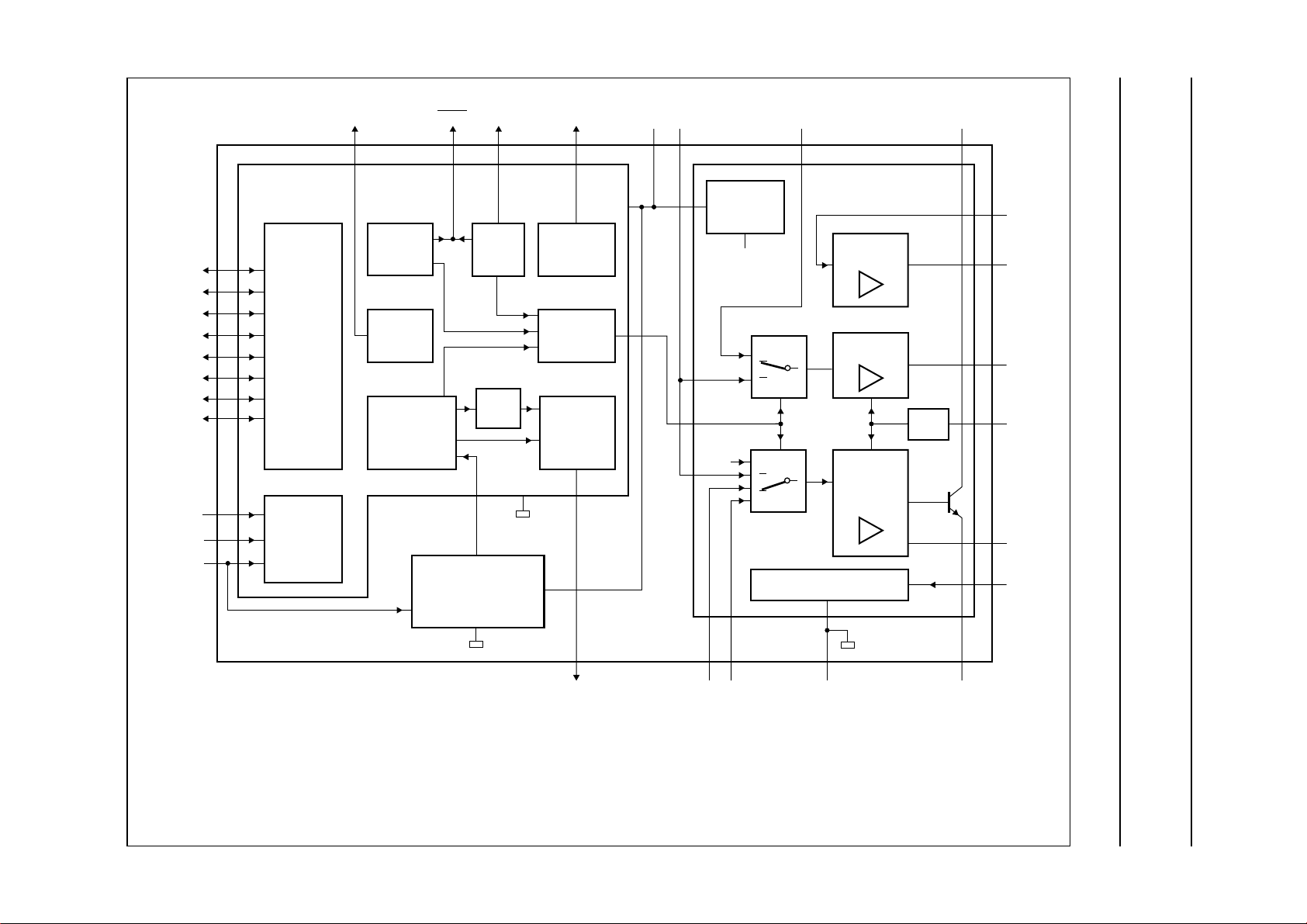
BLOCK DIAGRAM
Philips Semiconductors Product specification
One-chip telephone ICs with speech,
dialler and ringer functions
R1
R2
R3
R4
C1
C2
C3
C4
XTAL
CE/CSI
CE/FDI
DIALLER
PART
KEYBOARD
DETECTOR
TIMING/
CONTROL
FLASH
KEYTONE
TONE
GENERATOR
DMODP/FLKT
PULSE
dB
MDY
RINGER
PART
DETECTOR/
GENERATOR
LED
DTMF
INDICATION
MUTE
DTMF/
RINGER
V
DD
UBA205xx
DTMF
V
DD
REGULATOR
V
CC
SLPE
IR
SPEECH/TRANSMISSION
PART
EARPIECE
AMPLIFIER
RECEIVE
AMPLIFIER
TRANSMIT
AMPLIFIER
SUPPLY
AGC
LN
GAR
QR
RX
AGC
REG
V
FCA138
UBA2050(A); UBA2051(A;C)
CC
UBA2050 and UBA2050A: C4 output not available.
UBA2051 and UBA2051A: KT output not available.
UBA2050 and UBA2051: DMO output available, LED output not available.
UBA2050A and UBA2051A: LED output available, DMO output not available.
UBA2051C: KT output available, DMO and LED outputs not available.
MDY/TONE
Fig.1 Block diagram.
MIC+ MIC−
GND
SLPE
Philips Semiconductors Product specification
One-chip telephone ICs with speech,
UBA2050(A); UBA2051(A;C)
dialler and ringer functions
PINNING
SYMBOL
LN 11111positive line terminal
SLPE 22222slope (DC resistance) adjustment
REG 33333line voltage regulator decoupling
IR 44444receive amplifier input
AGC 55555automatic gain control and line-loss
DTMF 66666DTMF transmit input
V
DD
XTAL 88888oscillator input
DP/FL 99999dial pulse/flash output (active LOW)
DMO 10 − 10 −−dial mode output
LED − 10 − 10 − DTMF mode indication output
CE/CSI 11 11 11 11 11 chip enable/cradle switch input;
CE/FDI 12 12 12 12 12 chipenable/frequencydiscrimination
MDY/TONE 13 13 13 13 13 melody (ringer) output/DTMF
KT 14 14 −−10 keytone output
C4 −−14 14 14 keyboard input/output C4
C3 15 15 15 15 15 keyboard input/output C3
C2 16 16 16 16 16 keyboard input/output C2
C1 17 17 17 17 17 keyboard input/output C1
R4 18 18 18 18 18 keyboard input/output R4
R3 19 19 19 19 19 keyboard input/output R3
R2 20 20 20 20 20 keyboard input/output R2
R1 21 21 21 21 21 keyboard input/output R1
GND 22 22 22 22 22 negative line terminal
QR 23 23 23 23 23 earpiece amplifier output
GAR 24 24 24 24 24 gain adjustment earpiece amplifier
RX 25 25 25 25 25 receive amplifier output
MIC+ 26 26 26 26 26 non-inverting microphone amplifier
MIC− 27 27 27 27 27 inverting microphone amplifier input
V
CC
UBA2050 UBA2050A UBA2051 UBA2051A UBA2051C
77777stabilized supply for dialler and
28 28 28 28 28 supply for speech/transmission part
PIN
DESCRIPTION
compensation
ringer parts
note 1
input
generator output
input
and peripherals
Note
1. The cradle switch and the two positions ‘handset on the cradle’ and ‘handset lifted’ are further on in this document
referred to as ‘hook-switch’, respectively ‘on-hook’ and ‘off-hook’ position.
2000 May 19 6
Philips Semiconductors Product specification
One-chip telephone ICs with speech,
dialler and ringer functions
handbook, halfpage
MDY/TONE
LN
SLPE
REG
AGC
DTMF
V
DD
XTAL
DP/FL
DMO
CE/CSI
CE/FDI
KT
1
2
3
IR
4
5
6
7
UBA2050T
8
9
10
11
12
13
MGT042
V
28
CC
MIC−
27
MIC+
26
RX
25
GAR
24
23
QR
GND
22
21
R1
R2
20
R3
19
R4
18
C1
17
C2
16
1514
C3
handbook, halfpage
MDY/TONE
UBA2050(A); UBA2051(A;C)
LN
SLPE
REG
AGC
DTMF
V
DD
XTAL
DP/FL
LED
CE/CSI
CE/FDI
KT
1
2
3
IR
4
5
6
7
UBA2050AT
8
9
10
11
12
13
MGT043
V
28
CC
MIC−
27
MIC+
26
RX
25
GAR
24
23
QR
GND
22
21
R1
R2
20
R3
19
R4
18
C1
17
C2
16
1514
C3
Fig.2 Pin configuration (UBA2050T).
handbook, halfpage
MDY/TONE
LN
SLPE
REG
AGC
DTMF
V
DD
XTAL
DP/FL
DMO
CE/CSI
CE/FDI
C4
Fig.3 Pin configuration (UBA2050AT).
1
2
3
IR
4
5
6
7
UBA2051T
8
9
10
11
12
13
MGT044
V
28
CC
MIC−
27
MIC+
26
RX
25
GAR
24
23
QR
GND
22
21
R1
R2
20
R3
19
R4
18
C1
17
C2
16
1514
C3
handbook, halfpage
MDY/TONE
LN
SLPE
REG
AGC
DTMF
V
DD
XTAL
DP/FL
LED
CE/CSI
CE/FDI
C4
1
2
3
IR
4
5
6
7
UBA2051AT
8
9
10
11
12
13
MGT045
V
28
CC
MIC−
27
MIC+
26
RX
25
GAR
24
23
QR
GND
22
21
R1
R2
20
R3
19
R4
18
C1
17
C2
16
1514
C3
Fig.4 Pin configuration (UBA2051T).
2000 May 19 7
Fig.5 Pin configuration (UBA2051AT).
Philips Semiconductors Product specification
One-chip telephone ICs with speech,
dialler and ringer functions
handbook, halfpage
MDY/TONE
LN
SLPE
REG
AGC
DTMF
V
DD
XTAL
DP/FL
KT
CE/CSI
CE/FDI
C4
1
2
3
IR
4
5
6
7
UBA2051CT
8
9
10
11
12
13
FCA128
V
28
CC
MIC−
27
MIC+
26
RX
25
GAR
24
23
QR
GND
22
21
R1
R2
20
R3
19
R4
18
C1
17
C2
16
1514
C3
UBA2050(A); UBA2051(A;C)
The reference voltage can beincreased by connectingthe
resistorR
connecting the resistor RVA between pins REG and LN.
The voltage at pin REG is used by the internal regulator to
generate V
connected between pins REG and GND. This capacitor,
converted into an equivalent inductance (see Section “Set
impedance”), realizes the set impedance conversion from
its DC value (R
frequency range).
The voltage at pin SLPE is proportional to the line current,
and the voltage VLNat pin LN can be calculated as follows:
VLN=V
I
SLPE=Iline
where:
I
line
ICC= internal current consumption
IP= supply current for peripheral circuits
I
SUP
pin LN.
betweenpinsREGandSLPEordecreasedby
VA
and is decoupled by capacitor C
ref
SLPE
ref+RSLPE
− ICC− IP− I
) to its AC value (RCCin the audio
× I
SLPE
SUP
REG
= line current
= current consumed by the VDD regulator from
Fig.6 Pin configuration (UBA2051CT).
FUNCTIONAL DESCRIPTION
The values given in the functional description are typical
values unless otherwise specified.
For numbering of components, refer to Figs 7, 37 and 38.
Voltage levels are referenced to the negative line terminal
GND, except when otherwise specified.
Speech/transmission part
SUPPLY
The supply for the IC andits peripheral circuits is obtained
from the telephone line (see Fig.7).
Line interface (pins LN, SLPE and REG)
The IC generates a stabilized reference voltage V
ref
between pins LN and SLPE. This reference voltage is
4.15 V, is temperature compensated and can be adjusted
by means of an external resistor RVA.
Resistor R
pins SLPE and GND. The preferred value for R
20 Ω. Changing the value of R
is an external resistor connected between
SLPE
will affect more than
SLPE
SLPE
is
the DC characteristics: it also influences the microphone
and DTMF gains, the gain control characteristics, the
sidetone level and the maximum output swing on the line.
The DC current flowing into the set is determined by the
exchange supply voltage (V
resistance (R
(R
) and thereference voltage (V
line
), the DC resistance of the telephone line
exch
), the feeding bridge
exch
). The excesscurrent
ref
is shunted via pin LN to pin SLPE when the line current
(I
) is greater than the sum of the supply current of the
line
speech/transmission part (ICC), the current drawn by the
peripheral circuitry connected to VCC(IP) and the input
currentoftheVDDregulator(I
I
(9 mA), the internal referencevoltage (generating V
low
).Withlinecurrents below
SUP
ref
is automatically adjusted to a lower value.
This means that more sets can operate in parallel with
DC line voltages (excluding the polarity guard) down to an
absolute minimum voltage of 1.45 V. At line currents
below I
, the circuit has limited sending and receiving
low
levels. This is called the low voltage area.
)
2000 May 19 8

Philips Semiconductors Product specification
One-chip telephone ICs with speech,
dialler and ringer functions
Internal supply (pin VCC)
The internal transmission part circuitry is supplied from
VCC. This supply voltage is derived from the voltage on
pin LN by means of resistor RCC and must be decoupled
by capacitor C
This supply point may also be used to supply peripheral
circuits e.g. an electretmicrophone taking intoaccount the
supply possibilities according to Fig.8.
handbook, full pagewidth
R
V
connected between pins VCCand GND.
VCC
I
line
from preamp
exch
exch
R
line
SUPPLY TRANSMISSION PART
REG
LN
REGULATOR
SLPE
UBA2050(A); UBA2051(A;C)
The voltage V
consumed by the transmission part and the peripheral
circuits:
VCC=V
CC0
where:
V
CC0=VLN
I
= the current consumed by the output stage of the
REC
earpiece amplifier.
R
CC
V
CC
I
SUP
V
DD
GND
I
CC
(see Fig.9) depends on the current
CC
− RCC× (IP+I
− ICC× R
V
DIALLER/
RINGER
UBA205xx
CC
DD
REC
C
)
VCC
100
I
DD
ringer-
interface/
peripherals
µF
supply
electret
microphone
I
P
C
REG
4.7 µF
I
SLPE
R
SLPE
20 Ω
Fig.7 Supply configuration.
C
VDD
220
µF
FCA129
2000 May 19 9
Philips Semiconductors Product specification
One-chip telephone ICs with speech,
dialler and ringer functions
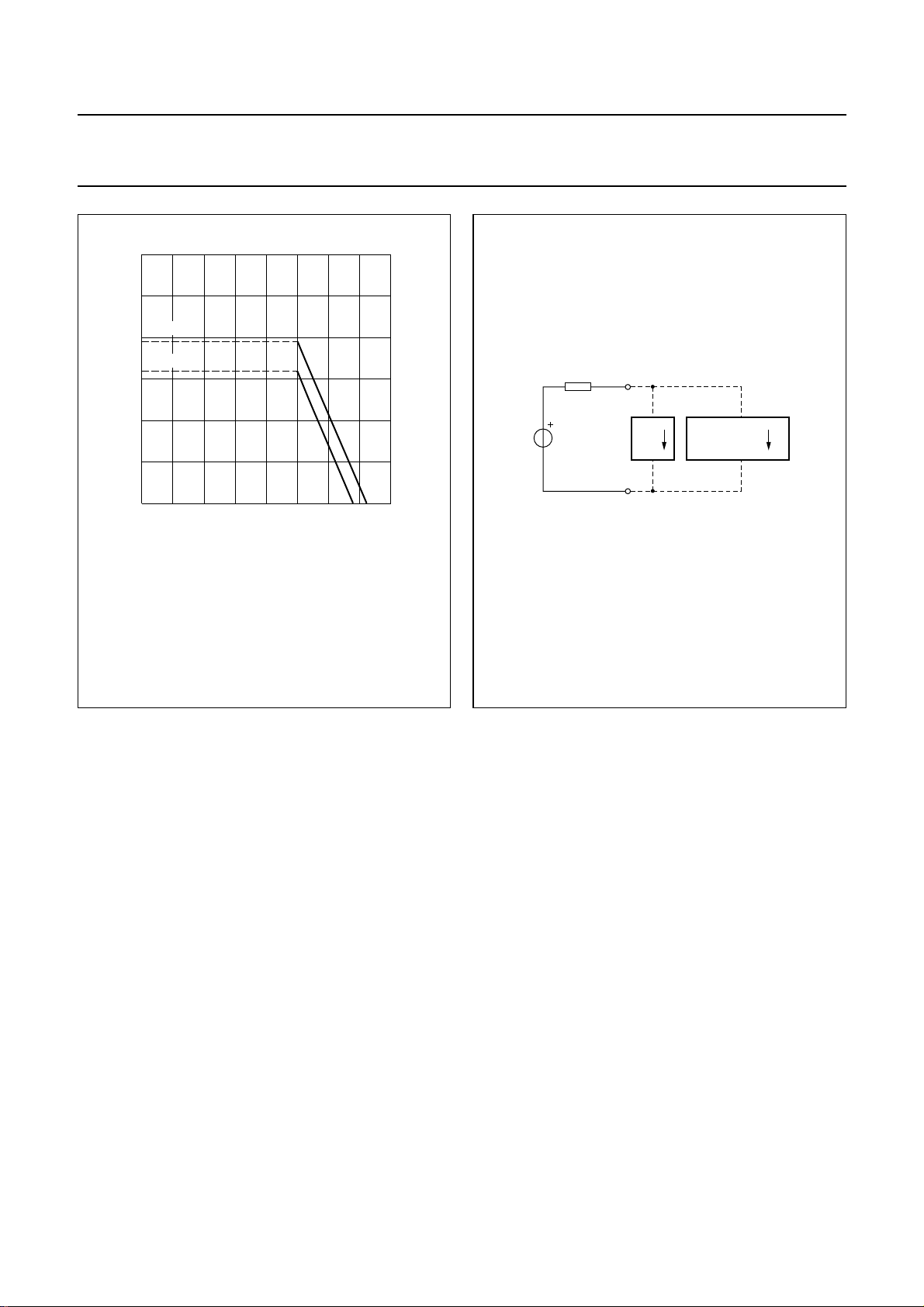
handbook, halfpage
3
I
P
(mA)
1.9 mA
2
1.6 mA
1
0
0
VCC≥ 2.5 V; VLN= 4.35 V at I
=20Ω.
R
SLPE
(1) This curve is valid when the receiving amplifier is not loaded.
(2) This curve is valid when the receiving amplifier is loaded;
V
o(rms)
12 43
= 15 mA; RCC= 619 Ω;
line
= 150 mV; RL= 150 Ω.
(2) (1)
MGL827
VCC (V)
handbook, halfpage
UBA2050(A); UBA2051(A;C)
V
R
CC0
CC
V
CC
GND
I
rec
PERIPHERAL
CIRCUITS
I
FCA130
P
Fig.8 Typical current IP available from VCC for
peripheral circuitry.
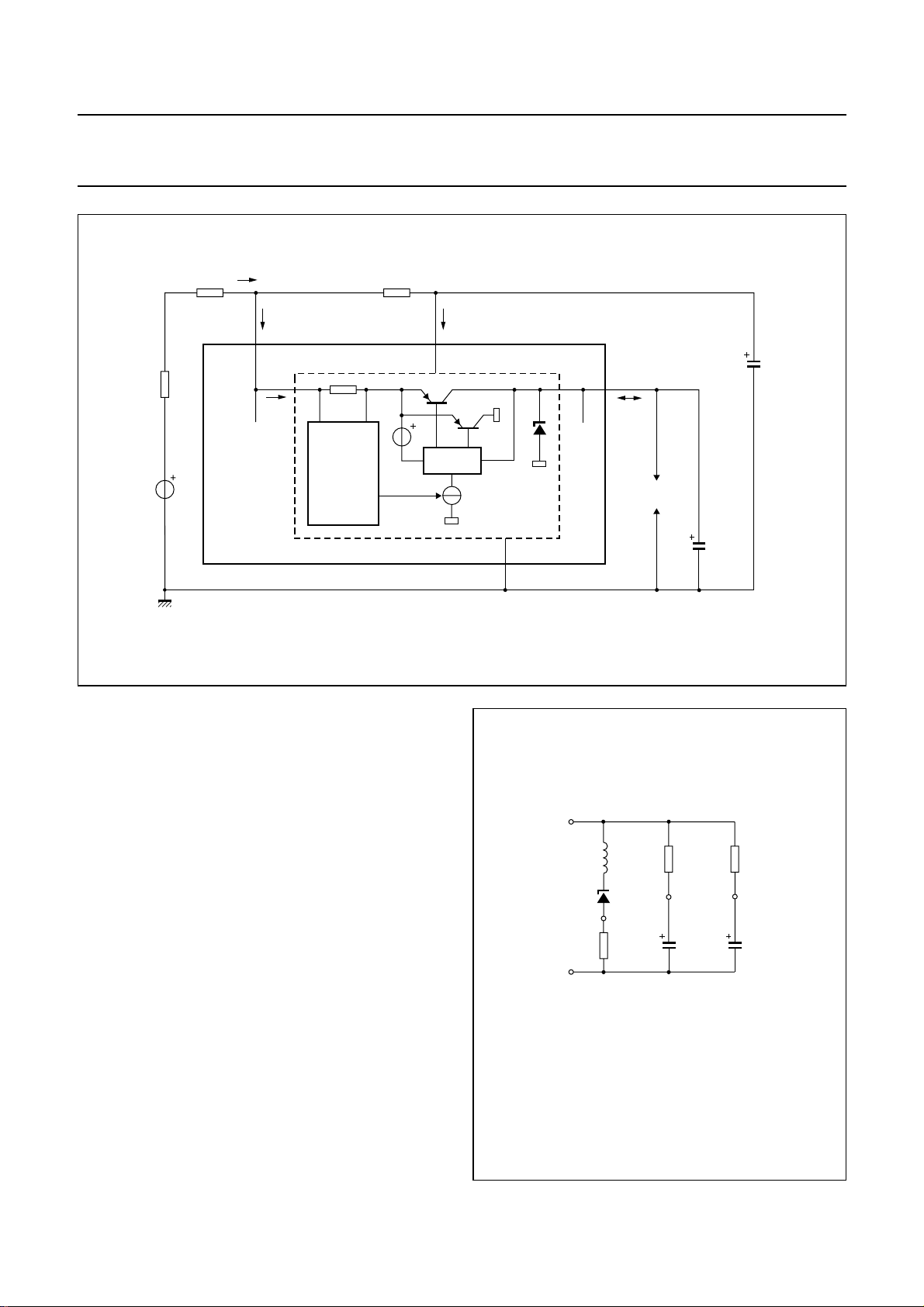
Regulated supply point (pin VDD)
The VDD regulator delivers a stabilized voltage to supply
the internal dialler and ringer parts and peripheral circuits
in transmission mode (nominal VLN) and in ringer mode
(VLN= 0 V). The maximum supply current for peripherals
is 1.9 mA in dialling mode (DTMF generator on) and
2.6 mA in speech mode (DTMF generator off). The supply
conditions in ringer and trickle (on-hook condition) modes
must not be disturbed by the peripheral supply currents.
Theregulator (see Fig.7) consistsofa sense input circuitry
(pin LN), a current switch and a VDD output stabilizer
(pin VDD). VDD is decoupled by capacitor C
VDD
.
Theregulatorfunctiondepends on the transmission, ringer
and trickle modes as follows:
• Transmissionmode:Theregulatoroperatesasacurrent
source at the LN input; it takes a constant current of
= 4.5 mA (at nominal conditions) from pin LN.
I
SUP
The current switch reduces the distortion on the line at
large signal swings.
Fig.9 VCC used as supply voltage for peripheral
circuits.
Output V
follows the DC voltage at pin LN (with
DD
typically 0.35 V difference) up to VDD= 3.3 V. The input
current of the regulator is constant while the output
(source) current is determined by the consumption of
the peripherals. The difference between input and
output current is shunted by the internal VDD stabilizer.
• Ringer mode: The regulator operates as a shunt
stabilizer to keep VDD at 3.3 V. The input voltage
VLNequals 0 V while the input current into pin VDD is
delivered by the ringing signal.
• Trickle mode: When VDD is below typically 2 V, the
regulator is inhibited. The current consumption of the
VDDregulator in trickle mode is very low to save most of
the trickle current for memory retention of the dialler and
ringer parts.
2000 May 19 10
Philips Semiconductors Product specification
One-chip telephone ICs with speech,
dialler and ringer functions
handbook, full pagewidth
R
exch
V
exch
R
line
UBA205xx
I
line
LN
I
SUP
I
LN
SENSE
R
CC
I
CC
V
CC
SWITCH
VDD regulator
GND
UBA2050(A); UBA2051(A;C)
C
VCC
V
DD
I
DD
peripherals
C
VDD
220 µF
100 µF
Fig.10 VDD regulator configuration.
SET IMPEDANCE
In the audio frequency range, the dynamic impedance is
mainly determined by resistor RCC. The equivalent
impedance of the circuit is illustrated in Fig.11.
handbook, halfpage
GND
LN
SLPE
L
EQ
V
ref
R
SLPE
20 Ω
FCA131
R
P
REG V
C
REG
4.7 µF
FCA132
R
CC
619 Ω
CC
C
VCC
100 µF
2000 May 19 11
LEQ=C
Internal resistance RP= 17.5 kΩ.
REG
× R
SLPE
× Rp.
Fig.11 Equivalent impedance between
LN and GND.
Philips Semiconductors Product specification
One-chip telephone ICs with speech,
dialler and ringer functions
TRANSMIT STAGES
Microphone signal amplification (pins MIC+ and MIC−)
The UBA205xx has symmetrical microphone inputs. The
input impedance between pins MIC+ and MIC− is 64 kΩ
(2 × 32 kΩ).
handbook, full pagewidth
(2)
MIC−
(1)
MIC+
UBA2050(A); UBA2051(A;C)
In speech mode, the voltage gain from pins MIC+ and
MIC− to pin LN is set at 44.2 dB at 600 Ω line load.
Microphone arrangements are illustrated in Fig.12.
Automatic gain control is provided on this amplifier for line
loss compensation.
V
CC
MIC−
MIC+
GND
MIC−
MIC+
MGT052
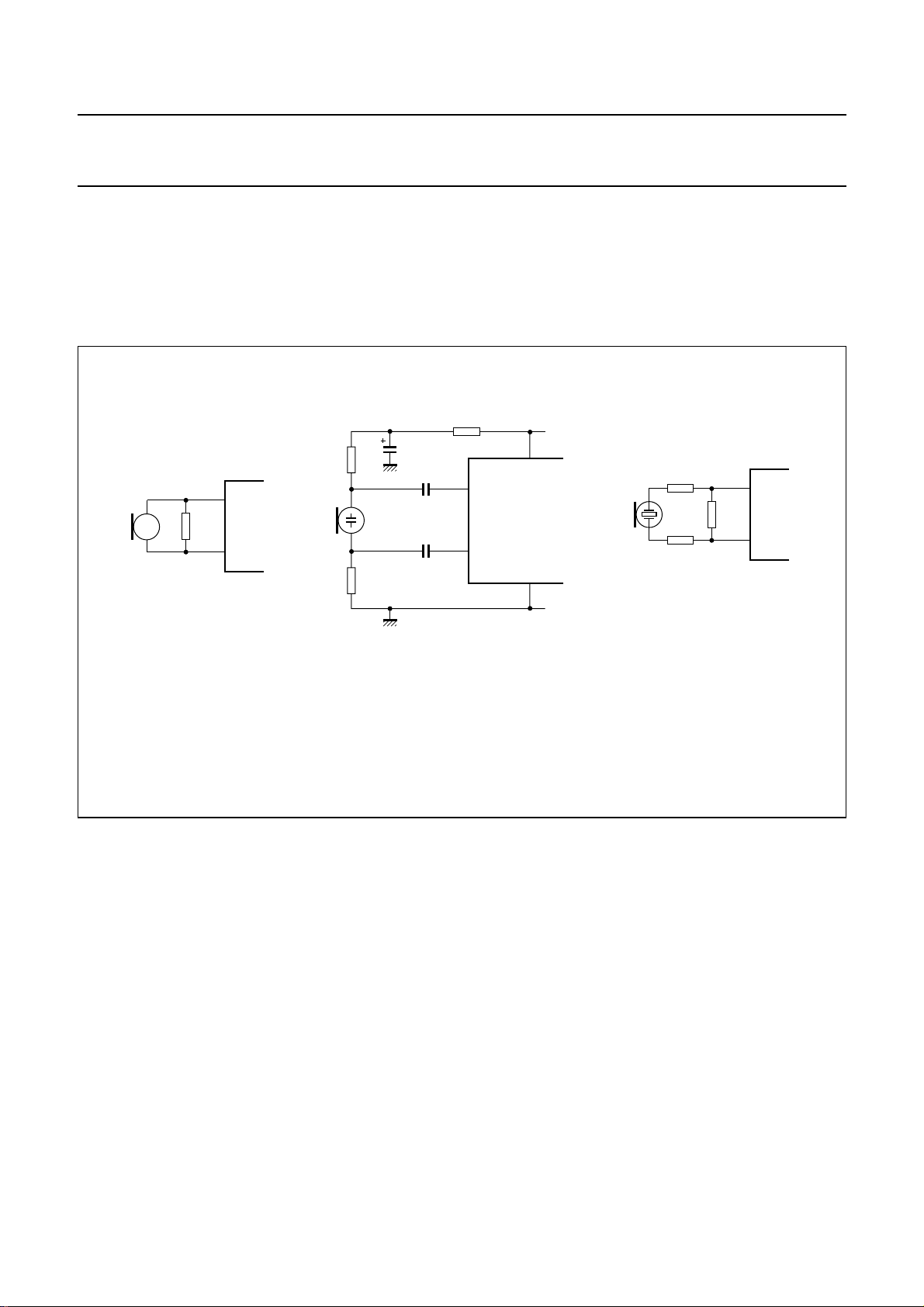
a. Magnetic or dynamic microphone. b. Electret microphone. c. Piezoelectric microphone.
(1) This resistor may be connected to reduce the terminating impedance.
(2) Extra decoupling capacitor for the microphone supply.
Fig.12 Microphone arrangements.
DTMF amplification (pin DTMF)
When the DTMF amplifier is enabled, dialling tones may
be sent on the line. These tones are generated at
pin MDY/TONE and their amplitude can be adjusted by
means of an attenuator and filter network (see Fig.35)
before being applied to the DTMF amplifier at pin DTMF.
The automatic gain control has no effect on the DTMF
amplifier.
RECEIVE STAGES
The receive part consists of a receive amplifier and an
earpiece amplifier.
Thesetonesarealso sent to the receive output RX atalow
level (confidence tone).
The UBA205xx has an asymmetrical DTMF input. The
input impedance between pins DTMF and GND is 20 kΩ.
The voltage gain from pin DTMF to pin LN is set at 26 dB
at 600 Ω line load. The DC voltage between pins DTMF
and GND is 0 V. So, when an external attenuator/filter
network is used, there is no need for a second decoupling
capacitor.
Receive amplifier (pins IR and RX)
The receive amplifier transfers the received signal from
input IR to output RX. The input impedance between
pins IR and GND is 20 kΩ.
The voltage gain from pin IR to pin RX is fixed at 33.4 dB.
The RX output is intended to drive high ohmic (real) loads.
Automatic gain control is provided on thereceive amplifier.
2000 May 19 12
Philips Semiconductors Product specification
One-chip telephone ICs with speech,
dialler and ringer functions
Earpiece amplifier (pins GAR and QR)
The earpiece amplifier is an operational amplifier having
its output QR and inverting input GAR available. It can be
used in conjunction with two resistors to get some extra
gain or attenuation.
Arrangements of the receive and earpiece amplifier are
illustrated in Fig.13. Earpiece connections are shown
in Fig.14.
In the basic configuration (see Fig.13), output RX drives
the earpiece amplifier by means of RE1 connected
between pins RX and the inverting input GAR. Feedback
resistor R
between pins QR and GAR. Output QR drives the
earpiece via a series capacitor C
The gain of the earpiece amplifier (from RX to QR) can be
set between +12 and −14 dB by means of resistor R
The preferred value of RE1 is 100 kΩ.
The earpiece amplifier offers a gain boost facility relative
to the initial gain. Resistor R
network of R
Cgb as shown in Fig.13.
of the earpiece amplifier is connected
GAR
.
ear
has to be replaced by the
GAR
GAR1,RGAR2
and Rgb and a series capacitor
GAR
UBA2050(A); UBA2051(A;C)
V
= ∞.
QR
---------V
RX
The initial gain is defined by:
which corresponds to R
gb
The gain boost is realised by a defined value of Rgband is
defined by:
+
V
QR
---------V
RX
R
GAR1RGAR2
--------------------------------------- -
R
E1
External capacitors C
QR and GAR) and C
GAR
GARS
+
×–=
1
(connected between pins
(connected between pins GAR
and GND) ensure stability. The capacitor C
first-order low-pass filter. The cut-off frequency
corresponds to the time constant C
of C
.
must be 10 times the value of C
GARS
stability.
The output voltages of the earpiece amplifier and the
DTMF amplifier are specified for continuous wave drive.
The maximum output voltage swing depends on the
DC line voltage VLN, the DC resistance RCC of the
set-impedance network between pins LN and VCC, the
current consumption ICCand IPfrom pin VCCand the load
impedance at pin QR.
R
GAR1RGAR2
–=
--------------------------------------- -
R
----------------------------------------- R
------------------------------------------
×
GAR1RGAR2
+
GAR1RGAR2
R
gb
GAR
× R
GAR
GAR
GAR
+
R
E1
provides a
. The value
to ensure
handbook, full pagewidth
V
R
exch
exch
I
line
UBA205xx
R
line
R
CC
EARPIECE
AMPLIFIER
R
GAR
C
CC
0.5V
CC
GAR
QRLN GAR
I
CC
V
GND
Fig.13 Receive and earpiece amplifier configuration.
2000 May 19 13
C
ear
C
R
E1
RX
C
100 µF
GARS
VCC
R
GAR2
Addition for gain boost of earpiece amplifier
earpiece
R
gb
C
gb
R
GAR1
C
GAR
C
GARS
R
E1
RXGARQR
FCA133
Philips Semiconductors Product specification
One-chip telephone ICs with speech,
dialler and ringer functions
handbook, full pagewidth
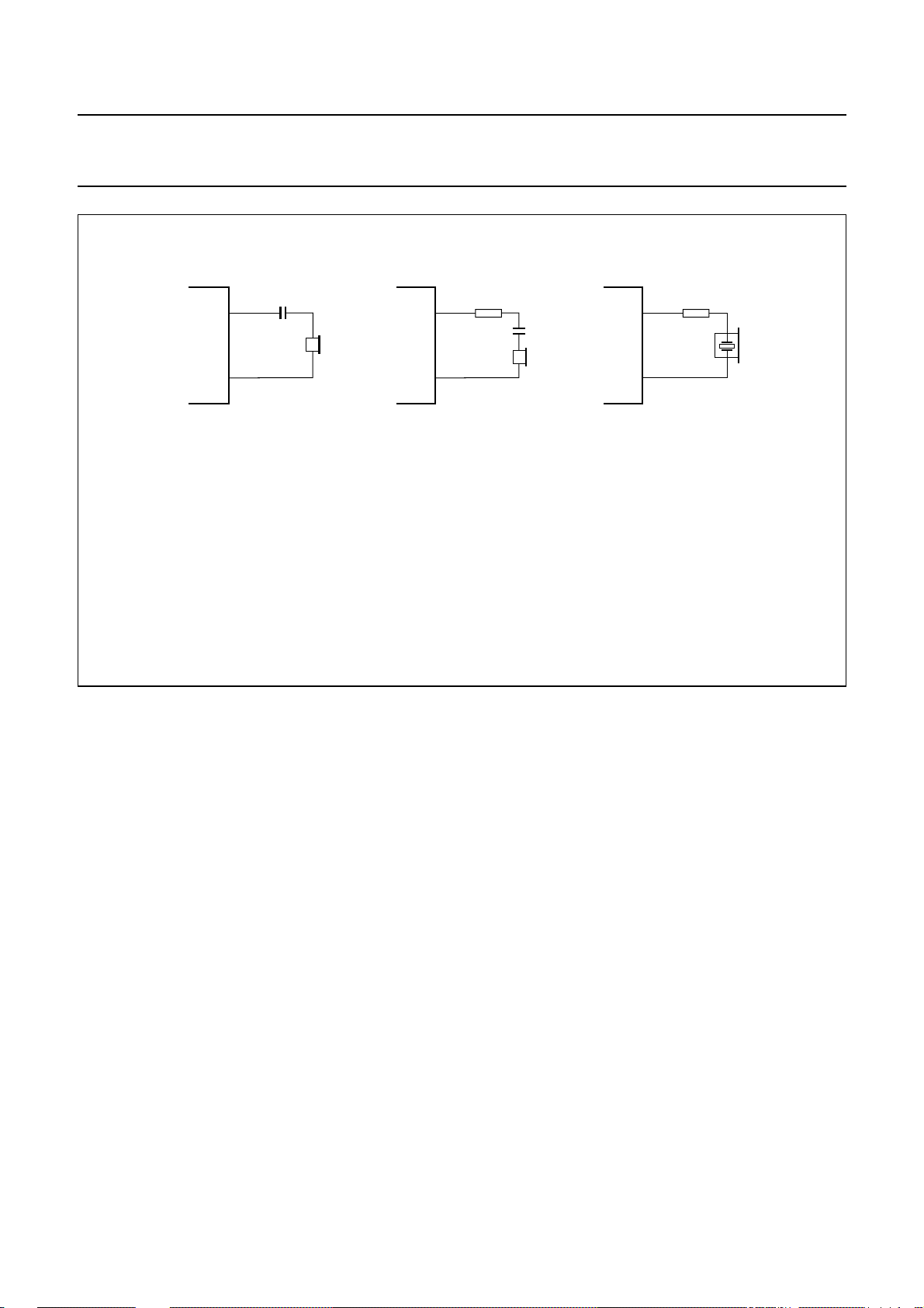
QR QR QR
a. Dynamic earpiece.
b. Magnetic earpiece.
UBA2050(A); UBA2051(A;C)
(1) (2)
GNDGNDGND
MGT051
c. Piezoelectric earpiece.
(1) This resistor may be connected to prevent distortion due to the inductive load.
(2) This resistor is required to increase the phase margin due to the capacitive load.
Fig.14 Earpiece connections.
2000 May 19 14
Philips Semiconductors Product specification
One-chip telephone ICs with speech,
dialler and ringer functions
AUTOMATIC GAIN CONTROL (PIN AGC)
The UBA205xx performs automatic line loss
compensation. The automatic gain control varies the gain
of the microphone amplifier and the gain of the receive
amplifier in accordance with the DC line current.
The control range is 6.0 dB. This corresponds
approximately to the lossfor a cable length of 5 km withan
0.5 mm diameter twisted copper-pair, a DC resistance of
176 Ω/km and an average attenuation of 1.2 dB/km).
handbook, full pagewidth
0
∆G
v
(dB)
−2
UBA2050(A); UBA2051(A;C)
The IC can be used with different configurations of
exchange supply voltage andfeeding bridge resistanceby
connecting an external resistor R
and GND (see Fig.15). This resistor enables the I
I
line currents to be increased (the ratio between I
stop
and I
is not affected by the resistor).
stop
The AGC function is disabled when pin AGC is left
open-circuit.
∞
R
=
AGC
between pins AGC
AGC
start
and
start
−4
−6
0 10 20 30 kΩ
I
line
Fig.15 Variation of gain as a function of line current with R
(mA)
as parameter.
AGC
10080604020 90705030100
MGT049
2000 May 19 15
Philips Semiconductors Product specification
One-chip telephone ICs with speech,
dialler and ringer functions
SIDETONE SUPPRESSION
The anti-sidetone network for the UBA205xx, comprising
RCCin parallel with Z
line,Rast1,Rast2,Rast3,RSLPE
(see Fig.16), suppresses the transmitted signal in the
earpiece. Maximum compensation is obtained when the
following conditions are fulfilled:
R
× R
k
Z
SLPE
=
bal
ast1=RCC
R
-----------------------------------------------------------
=k×Z
R
ast2
R
ast1RSLPE
line
× (R
+()×
ast3RSLPE
×
ast2+Rast3
)
The scale factor k is chosen to meet the compatibility with
a standard capacitor from the E6 or E12 range for Z
In practice, Z
the line length. Therefore, the value of Z
varies considerably with the line type and
line
bal
chosenfor an average linelength, which gives satisfactory
sidetone suppression with short and long lines.
and Z
should be
bal
bal
.
UBA2050(A); UBA2051(A;C)
The suppression also depends on the accuracy of the
match between Z
line.
The anti-sidetone network for the UBA205xx attenuates
the received signal from the line by 32 dB before it enters
the receive stage. The attenuation is almost constant over
the whole audio frequency range.
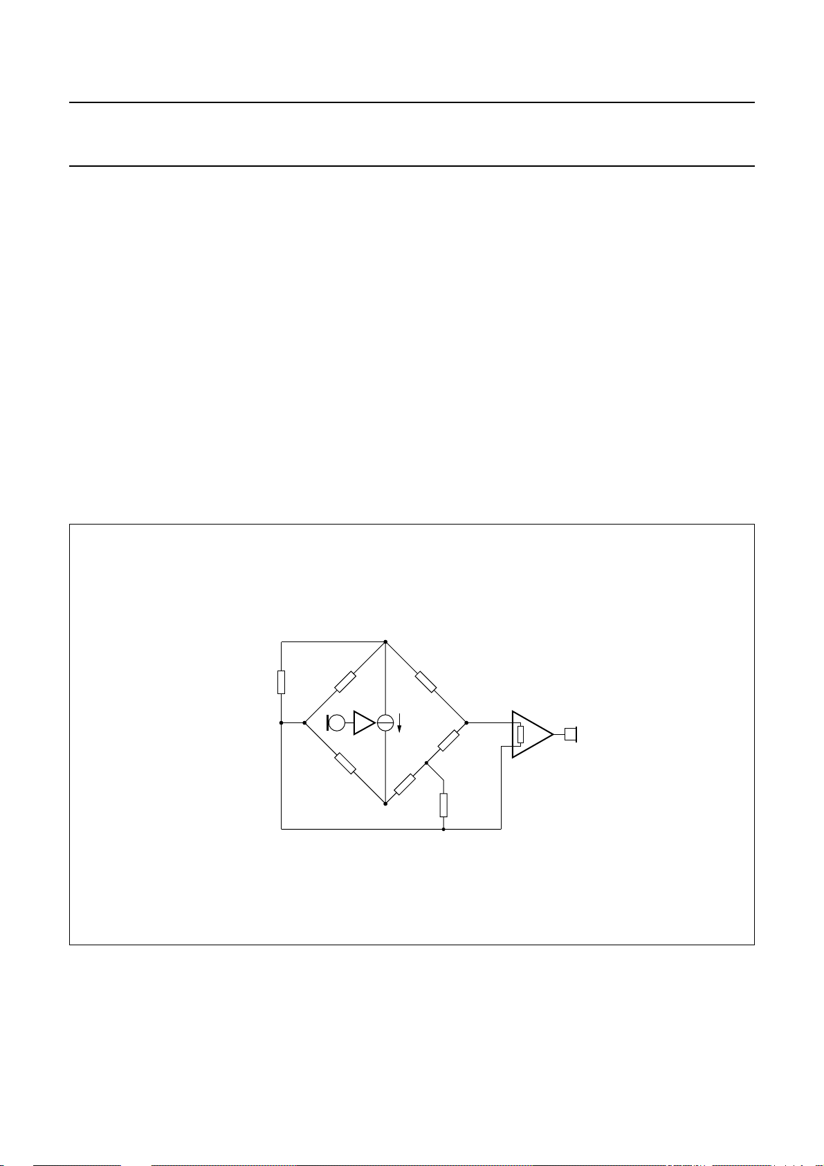
A Wheatstone bridge configuration (see Fig.17) may also
be used.
More information on the balancing of an anti-sidetone
bridge can be obtained in our publication
Handbook for Wired Telecom Systems, IC03b”
and the impedance of the average
bal
“Application
.
handbook, full pagewidth
LN
Z
line
GND
R
SLPE
R
CC
SLPE
R
ast1
I
m
R
ast3
IR
Z
R
ast2
Z
bal
MGT046
ir
Fig.16 Equivalent circuit of UBA205xx anti-sidetone bridge.
2000 May 19 16
 Loading...