

Philips uba2030t DATASHEETS

INTEGRATED CIRCUITS
DATA SH EET
UBA2030T
Full bridge driver IC
Preliminary specification
Supersedes data of 1997 Sep 16
File under Integrated Circuits, IC11
1999 Aug 10

Philips Semiconductors Preliminary specification
Full bridge driver IC UBA2030T
FEATURES
• Full bridge driver
• Integrated bootstrap diodes
• Integrated high voltage level shift function
• High voltage input (570 V maximum) for the internal
supply
• Adjustable ‘dead time’
• Adjustable oscillator frequency
• High voltage level shifter for the bridge enable function
• Shut-down function.
APPLICATIONS
• The UBA2030T can drive the MOSFETs in any type of
load configured as a full bridge
• The circuit is intended as a commutator for High
Intensity Discharge (HID) lamps.
ORDERING INFORMATION
TYPE NUMBER
NAME DESCRIPTION VERSION
UBA2030T SO24 plastic small outline package; 24 leads; body width 7.5 mm SOT137-1
GENERAL DESCRIPTION
The UBA2030T is a high voltage integrated circuit
fabricated using the BCD750 power logic process.
The circuit is designed for driving the MOSFETs in a full
bridge configuration. In addition, it features a shut-down
function,anadjustableoscillatorandaPMOShighvoltage
level shifter to control the bridge enable function.
To guarantee an accurate 50% duty factor, the oscillator
signal passes through a divider before being fed to the
output drivers.
PACKAGE
1999 Aug 10 2
Philips Semiconductors Preliminary specification
Full bridge driver IC UBA2030T
QUICK REFERENCE DATA
SYMBOL PARAMETER CONDITIONS MIN. TYP. MAX. UNIT
High voltage
V
HV
Start-up; powered via pin HV
I
strtu
V
th(osc strt)
V
th(osc stp)
Output drivers
I
o(source)
I
o(sink)
Internal oscillator
f
bridge
External oscillator
f
osc(ext)
high voltage supply 0 − 570 V
start-up current − 0.7 1.0 mA
start oscillating threshold
at f
= 500 Hz; no load 14.0 15.5 17.0 V
bridge
voltage
stop oscillating threshold voltage 11.5 13.0 14.5 V
output source current VDD=V
V
GHR=VGHL=VGLR=VGLL
output sink current VDD=V
V
GHR=VGHL=VGLR=VGLL
FSL=VFSR
FSL=VFSR
=15V;
=15V;
140 190 240 mA
=0V
200 260 320 mA
=15V
bridge oscillating frequency EXO pin connected to SGND 50 − 50000 Hz
external oscillator frequency RC pin connected to SGND; 100 − 100000 Hz
f
=
osc(ext)
----------------2
f
bridge
Dead time control
t
dead
dead time control range
(adjusted externally)
Bridge enable
I
IH
I
IL
HIGH-level input current bridge enable active 100 − 700 µA
LOW-level input current bridge enable not active 0 − 20 µA
Shut-down
V
IH
V
IL
HIGH-level input voltage
LOW-level input voltage shut-down not active; 0 − 0.5 V
shut-down active;
∆V
SD
--------------
5 V/ms>
∆t
∆ V
SD
-------------∆t
0.4 − 4 µs
5 V/ms>
4.5 − V
DD
V
1999 Aug 10 3
Philips Semiconductors Preliminary specification
Full bridge driver IC UBA2030T
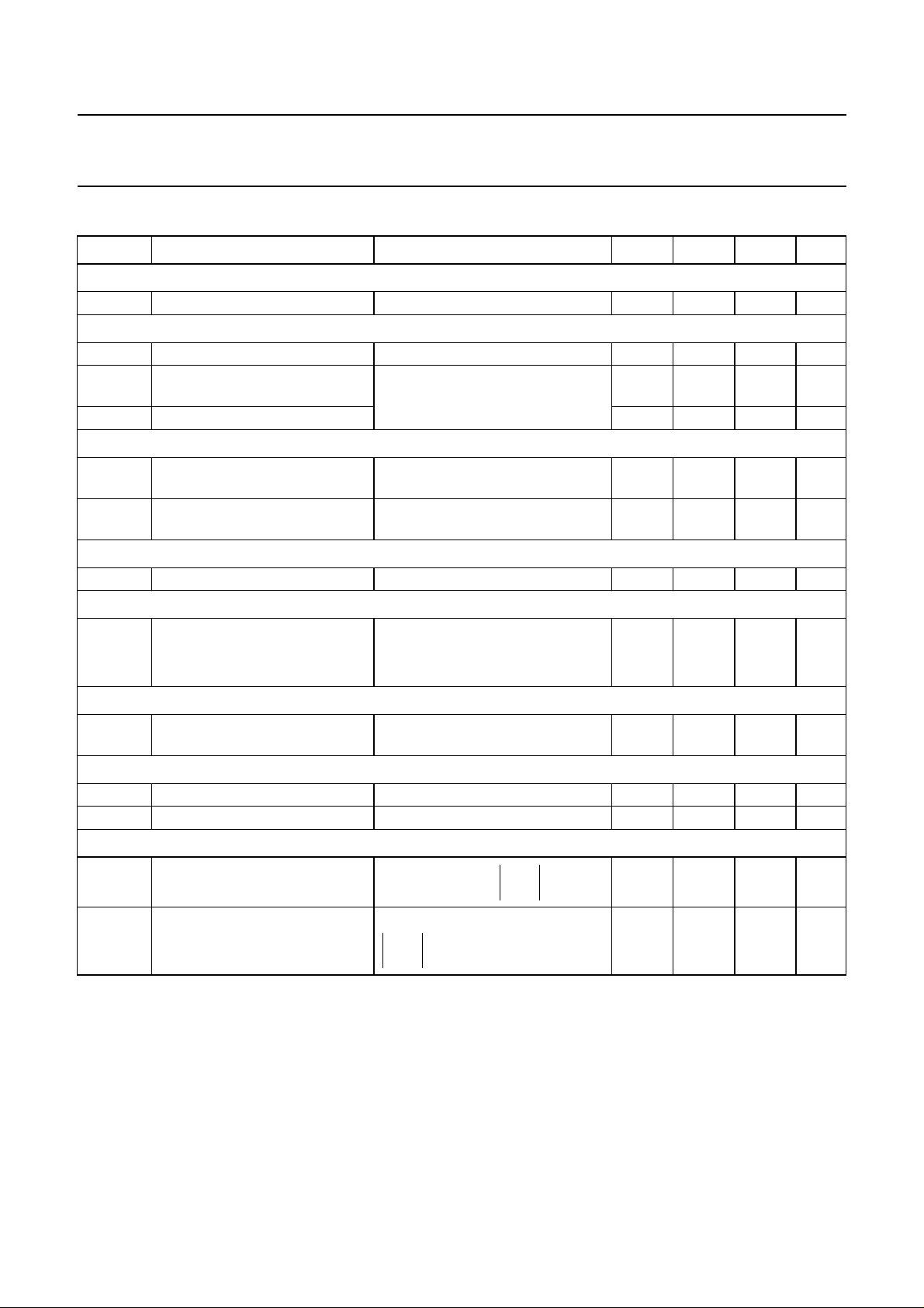
BLOCK DIAGRAM
handbook, full pagewidth
HV BER BE
18
LOW VOLTAGE
SUPPLY
24 23 5 20 22
SGND VDDRC EXO DTC
87
BRIDGE ENABLE
OSCILLATOR
÷ 2
LOGIC
21
SD
Fig.1 Block diagram.
HIGH VOLTAGE
LEVEL SHIFTER
UBA2030T
LOW VOLTAGE
LEVEL SHIFTER
HIGHER LEFT
HIGHER RIGHT
LOWER LEFT
LOWER RIGHT
4, 6, 9, 16, 17, 19
n.c.
DRIVER
DRIVER
DRIVER
DRIVER
10
11
12
15
14
13
MGK590
FSL
GHL
SHL
FSR
GHR
SHR
3
GLL
2
PGND
1
GLR
1999 Aug 10 4
Philips Semiconductors Preliminary specification
Full bridge driver IC UBA2030T
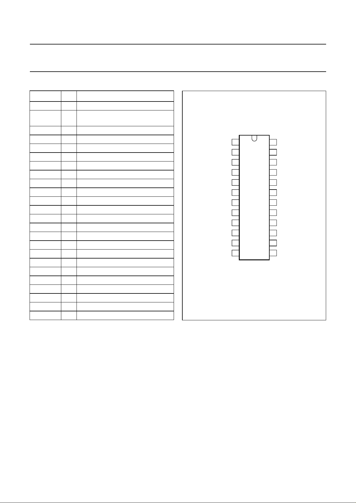
PINNING
SYMBOL PIN DESCRIPTION
GLR 1 gate of lower right MOSFET
PGND 2 power ground for sources of lower
left and right MOSFETs
GLL 3 gate of lower left MOSFET
n.c. 4 not connected
RC 5 RC input for internal oscillator
n.c. 6 not connected
BE 7 bridge enable control input
BER 8 bridge enable reference input
n.c. 9 not connected
FSL 10 floating supply voltage left output
GHL 11 gate of higher left MOSFET
SHL 12 source of higher left MOSFET
SHR 13 source of higher right MOSFET
GHR 14 gate of higher right MOSFET
FSR 15 floating supply voltage right output
n.c. 16 not connected
n.c. 17 not connected
HV 18 high voltage supply input
n.c. 19 not connected
EXO 20 external oscillator input
SD 21 shut-down input
DTC 22 ‘dead time’ control input
V
DD
23 internal (low voltage) supply
SGND 24 signal ground
handbook, halfpage
GLR
1
PGND
2
GLL
3
n.c.
4
RC
5
n.c.
6
UBA2030T
BE
7
8
BER
n.c.
9
FSL
10
GHL
11
SHL
12
MGK589
Fig.2 Pin configuration.
SGND
24
V
23
DD
DTC
22
SD
21
EXO
20
19
n.c.
HV
18
17
n.c.
n.c.
16
FSR
15
GHR
14
SHR
13
1999 Aug 10 5

Philips Semiconductors Preliminary specification
Full bridge driver IC UBA2030T
FUNCTIONAL DESCRIPTION
Supply voltage
The UBA2030T is powered by a single supply voltage
connected to the HV pin (the full bridge supply could be
used, for example). The IC generates its own low voltage
supply for driving the internal circuitry and the MOSFETs
in the full bridge, removing the need for an additional low
voltage supply. A capacitor must be connected between
the VDDpin and SGND to obtain a ripple-free internal
supply voltage.
Start-up
When the power is turned on, the UBA2030T enters a
start-up phase; the high side MOSFETs are switched off
and the low side MOSFETs switched on. During start-up,
thebootstrapcapacitorsarecharged and the bridgeoutput
current is zero.
Oscillation
Atthepointwherethe supply voltage at theHV pincrosses
the ‘start oscillating threshold’, the bridge begins
commutating between the following two defined states:
Higher left and lower right MOSFETs on,
higher right and lower left MOSFETs off
Higher left and lower right MOSFETs off,
higher right and lower left MOSFETs on.
When the internal oscillator is used, the bridge
commutating frequency is determined by the values of an
external resistor and capacitor. In this mode, the EXO pin
must be connected to SGND.
When an external oscillator is used, its output must be
connected to the EXO pin; the internal oscillator must be
disabled by connecting the RC pin to SGND. The bridge
commutatingfrequency is half the oscillator frequency due
to a ÷2 circuit which guarantees an accurate 50% duty
factor.
The time between turning off the conducting pair of
MOSFETs and turning on the other pair, the ‘dead time’,
can be adjusted using an external resistor. If the supply
voltage at the HV pin falls below the ‘stop oscillating
threshold’, the UBA2030T re-enters the start-up phase.
Bridge enable
The bridge enable function allows the bridge to be held in
its current state. When active, it connects the RC pin to
SGND,disablingtheinternaloscillator.Ifthebridge enable
function is activated during ‘dead time’, the bridge is
allowed to enter the next conducting state before being
held. Oscillations resume the instant the bridge enable
function is turned off. A timing diagram is shown in Fig.3.
To hold the bridge, an external control circuit is required to
provide a source current to the bridge enable control input
(pin BE), and to supply a reference voltage to pin BER,
(see Fig.6).
Shut-down
The active HIGH shut-down input (pin SD) can be used at
any time to turn off all four MOSFETs. However, if the
supply voltage drops below the ‘stop oscillating threshold’,
the bridge re-enters the start-up phase even if the
shut-down function is active.
1999 Aug 10 6
 Loading...