

Philips UBA2021T, UBA2021P Datasheet

INTEGRATED CIRCUITS
DATA SH EET
UBA2021
630 V driver IC for CFL and TL
lamps
Product specification
Supersedes data of 2000 Jul 24
File under Integrated Circuits, IC11
2001 Jan 30
Philips Semiconductors Product specification
630 V driver IC for CFL and TL lamps UBA2021
FEATURES
• Adjustable preheat and ignition time
• Adjustable preheat current
• Adjustable lamp power
• Lamp temperature stress protection at higher mains
GENERAL DESCRIPTION
The UBA2021 is a high-voltage IC intended to drive and
control Compact Fluorescent Lamps (CFL) or fluorescent
TL-lamps. It contains a driver circuit for an external
half-bridge, an oscillator and a control circuit for starting
up, preheating, ignition, lamp burning and protection.
voltages
• Capacitive mode protection
• Protection against a too-lowdrive voltage for the power
MOSFETs.
QUICK REFERENCE DATA
SYMBOL PARAMETER CONDITIONS MIN. TYP. MAX. UNIT
High voltage supply
V
FS
high side supply voltage IFS<15µA; t < 0.5 s −−630 V
Start-up state
V
VS(start)
V
VS(stop)
I
VS(standby)
oscillator start voltage − 11.95 − V
oscillator stop voltage − 10.15 − V
standby current VVS=11V − 200 −µA
Preheat mode
f
start
t
ph
V
RS(ctrl)
start frequency − 108 − kHz
preheat time CCP= 100 nF − 666 − ms
control voltage at pin RS −−600 − mV
Frequency sweep to ignition
f
B
t
ign
bottom frequency − 42.9 − kHz
ignition time − 625 − ms
Normal operation
f
B
t
no
I
tot
, R
R
G1(on)
R
, R
G1(off)
bottom frequency − 42.9 − kHz
non-overlap time − 1.4 −µs
total supply current fB= 43 kHz − 1 − mA
high and low side on resistance − 126 −Ω
G2(on)
high and low side off resistance − 75 −Ω
G2(off)
Feed-forward
f
ff
I
i(RHV)
feed-forward frequency I
= 0.75 mA − 63.6 − kHz
RHV
I
= 1.0 mA − 84.5 − kHz
RHV
operating range of input current at pin RHV 0 − 1000 µA
2001 Jan 30 2
Philips Semiconductors Product specification
630 V driver IC for CFL and TL lamps UBA2021
ORDERING INFORMATION
TYPE NUMBER
PACKAGE
NAME DESCRIPTION VERSION
UBA2021T SO14 plastic small outline package; 14 leads; body width 3.9 mm SOT108-1
UBA2021P DIP14 plastic dual in-line package; 14 leads (300 mil) SOT27-1
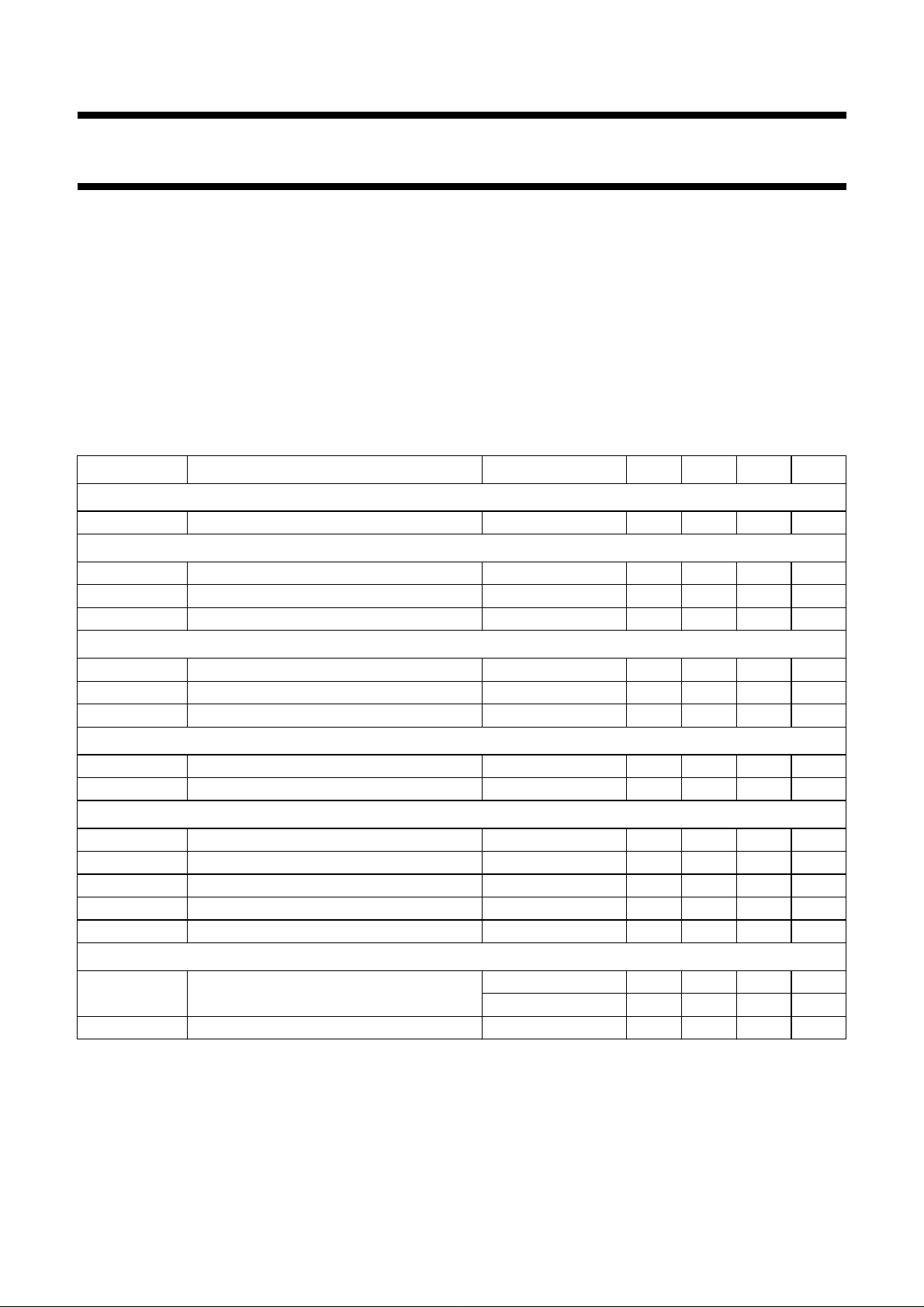
BLOCK DIAGRAM
CI
CF
handbook, full pagewidth
n.c.
4
VS
RHV
5
SUPPLY
BAND GAP
REFERENCE
13
RREF
12
10
OSCILLATOR
14
SB
LEVEL
SHIFTER
bootstrap
charging circuit
HIGH SIDE
DRIVER
1
FS
2
G1
3
S1
CP
RS
8
9
RS
MONITOR
TIMING
CONTROL
NON
OVERLAP
UBA2021
LOW SIDE
DRIVER
11
SGND
MGS988
6
G2
7
PGND
Fig.1 Block diagram.
2001 Jan 30 3

Philips Semiconductors Product specification
630 V driver IC for CFL and TL lamps UBA2021
PINNING
SYMBOL PIN DESCRIPTION
FS
G1
S1
n.c.
VS
G2
PGND
CP
RS
RREF
SGND
CF
RHV
CI
1
2
3
4
5
6
7
8
9
10
11
12
13
14
high side floating supply voltage
gate high transistor (T1)
source high transistor (T1)
high-voltage spacer, not to be connected
low voltage supply
gate low transistor (T2)
power ground
timing/averaging capacitor
current monitoring input
reference resistor
signal ground
oscillator capacitor
start-up resistor/feed-forward resistor
integrating capacitor
handbook, halfpage
FS
G1
S1
n.c.
VS
G2
PGND
1
2
3
4
UBA2021T
5
6
7
MGS989
14
CI
13
RHV
12
CF
11
SGND
10
RREF
9
RS
8
CP
Fig.2 Pin configuration (SO14).
2001 Jan 30 4
handbook, halfpage
FS
G1
S1
n.c.
VS
G2
PGND
1
2
3
4
UBA2021P
5
6
7
MGS990
14
CI
13
RHV
12
CF
11
SGND
10
RREF
9
RS
8
CP
Fig.3 Pin configuration (DIP14).

Philips Semiconductors Product specification
630 V driver IC for CFL and TL lamps UBA2021
FUNCTIONAL DESCRIPTION
Introduction
The UBA2021 is an integrated circuit for electronically
ballasted compact fluorescent lamps and their derivatives
operating with mains voltages up to 240 V (RMS). It
provides all the necessary functions for preheat, ignition
and on-state operation of the lamp. In addition to the
control function, the IC provides level shift and drive
functions for the two discrete power MOSFETs, T1 and T2
(see Fig.7).
Initial start-up
Initial start-up is achieved by charging capacitor CS9 with
the current applied to pin RHV. At start-up, MOSFET T2
conducts and T1 is non-conducting, ensuring C
boot
becomes charged. This start-up state is reached for a
supply voltage V
VS(reset)
(this is the voltage level at pin VS
at which the circuit will be reset to the initial state) and
maintained until the low voltage supply (VVS) reaches a
value of V
. The circuit is reset in the start-up state.
VS(start)
Oscillation
When the low voltage supply (VVS) has reached the value
of V
VS(start)
the circuit starts oscillating in the preheat state.
The internal oscillator is a current-controlled circuit which
generates a sawtooth waveform. The frequency of the
sawtooth is determined by the capacitor CCF and the
current out of pin CF (mainly set by R
). The sawtooth
RREF
frequency is twice the frequency of the signal across the
load. The IC brings MOSFETs T1 and T2 alternately into
conduction with a duty factor of approximately 50%.
Figure 4 represents the timing of the IC. The circuit block
'non-overlap' generates a non-overlap time tno that
ensures conduction periods of exclusively T1 or T2. Time
tno is dependent on the reference current I
RREF
.
handbook, halfpage
V
CF
0
internal
clock
0
V
(G1-S1)
0
V
(G2)
0
start-up
t
no
MGS991
t
no
time
Fig.4 Oscillator timing.
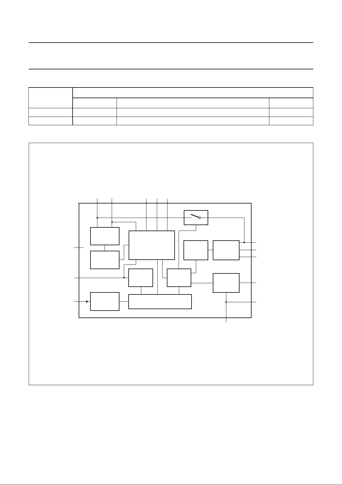
Operation in the preheat mode
The circuit starts oscillating at approximately 2.5 × f
B
(108 kHz). The frequency gradually decreases until a
defined value of current I
is reached (see Fig.5). The
shunt
slope of the decrease in frequency is determined by
capacitor CCI. The frequency during preheating is
approximately 90 kHz. This frequency is well above the
resonantfrequencyofthe load, which means that the lamp
is off; the load consists of L2, C5 and the electrode
resistance only. The preheat time is determined by
capacitor CCP. The circuit can be locked in the preheat
state by connecting pin CP to ground. During preheating,
the circuit monitors the load current by measuring the
voltage drop over external resistor R
conduction of T2 with decision level V
frequency is decreased as long as VRS>V
frequency is increased for VRS<V
shunt
RS(ctrl)
RS(ctrl)
at the end of
. The
. The
RS(ctrl)
.
2001 Jan 30 5
Philips Semiconductors Product specification
630 V driver IC for CFL and TL lamps UBA2021
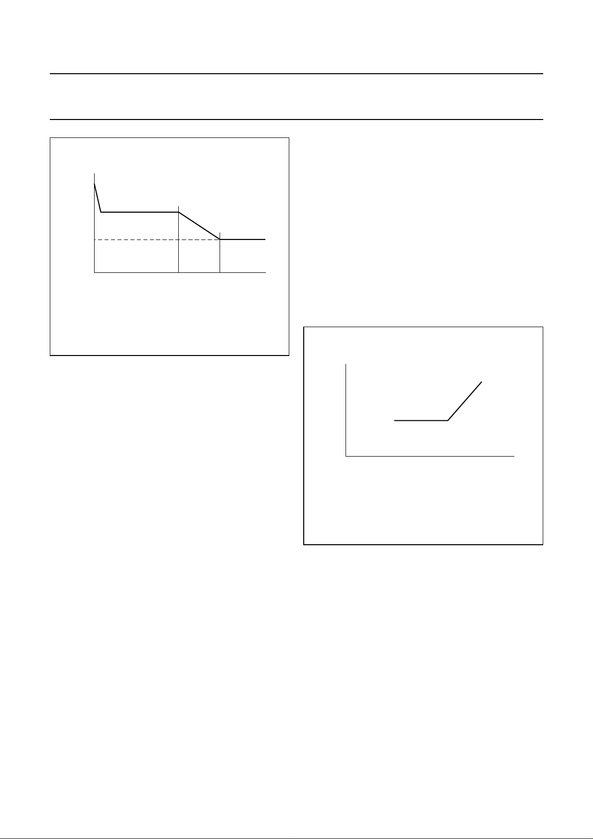
Feed-forward frequency
Above a defined voltage level the oscillation frequency
handbook, halfpage
f
start
f
B
preheat state
For calculations refer to Chapter “Design equations”.
ignition
state
Fig.5 Operation in the preheat mode.
MGS992
burn state
time
also depends on the supply voltage of the half-bridge
(see Fig.6).Thecurrentforthecurrent-controlled oscillator
is in the feed-forward range derived from the current
through R
tothe average value of the current through R
operating range of I
. The feed-forward frequency is proportional
RHV
withinthe
RHV
, given the lower limit set by fB.
i(RHV)
For currents beyond the operating range (i.e. between
1.0 and 1.6 mA)thefeed-forwardfrequencyisclamped.In
order to prevent feed-forward of ripple on Vin, the ripple is
filtered out. The capacitor connected to pin CP is used for
this purpose. This pin is also used in the preheat state and
the ignition state for timing (tphand t
ign
).
Ignition state
The RS monitoring function changes from V
RS(ctrl)
regulation to capacitive mode protection at the end of the
preheat time. Normally this results in a further frequency
decrease down to the bottom frequency fB(approximately
43 kHz). The rate of change of frequency in the ignition
state is less than that in the preheat mode. During the
downward frequency sweep, the circuit sweeps through
the resonant frequency of the load. A high voltage then
appears across the lamp. This voltage normally ignites the
lamp.
Failure to ignite
Excessive current levels may occur if the lamp fails to
ignite. The IC does not limit these currents in any manner.
Transition to the burn state
Assuming that the lamp has ignited during the downward
frequencysweep,thefrequencynormallydecreasestothe
bottom frequency. The IC can transit to the burn state in
two ways:
1. In the event that the bottom frequency is not reached,
transition is made after reaching the ignition time t
ign
2. As soon as the bottom frequency is reached.
The bottom frequency is determined by R
RREF
and CCF.
handbook, halfpage
f
(kHz)
feed-forward
range
bottom
frequency
I
(mA)
RHV
For calculations refer to Chapter “Design equations”.
Fig.6 Feed-forward frequency.
Capacitive mode protection
When the preheat mode is completed, the IC will protect
the power circuit against losing the zero voltage switching
condition and getting too close to the capacitive mode of
operation. This is detected by monitoring voltage VRS at
pin RS. If the voltage is below V
RS(cap)
at the time of
turn-onof T2, then capacitive mode operation is assumed.
Consequently the frequency increases as long as the
.
capacitive mode is detected. The frequency decreases
down to the feed-forward frequency if no capacitive mode
is detected. Frequency modulation is achieved via pin CI.
MGS993
2001 Jan 30 6
 Loading...