


INTEGRATED CIRCUITS
DATA SH EET
UBA1710M
Modulator for GaAs power
amplifiers
Product specification
Supersedes data of 1997 Feb 18
File under Integrated Circuits, IC17
1997 Oct 17
Philips Semiconductors Product specification
Modulator for GaAs power amplifiers UBA1710M
FEATURES
• Power MOS modulators for control of GaAs power
amplifier drain voltage
• Power control loop amplifier and MOS driver
• Voltage tripler for supply of MOS driver
• Positive-to-negative DC converter for GaAs power
amplifier gate biasing.
APPLICATIONS
• Control of GaAs power amplifiers for GSM and DCS
hand-held transceivers.
QUICK REFERENCE DATA
SYMBOL PARAMETER
V
CC
V
DD
I
CC+IDD
T
amb
analog supply voltage 4.2 4.8 7.5 V
digital supply voltage 4.2 4.8 7.5 V
peak supply current in power-up mode − 12 − mA
operating ambient temperature −20 − +85 °C
Note
1. For conditions, see Chapter “Characteristics”.
(1)
GENERAL DESCRIPTION
The UBA1710M integrates the functions required to
operate the GaAs Power Amplifiers (PAs) from the
CGY20xx family which are intended for GSM and DCS
applications.
It includes a negative supply for PA gate biasing and most
of the functions required to implement power control so
that only a very few external component are required.
The power control section integrates two power MOS
devices for control of the PA drain voltages, an MOS driver
and a feedback loop amplifier. The MOS driver is supplied
from an on-chip voltage tripler.
MIN. TYP. MAX. UNIT
ORDERING INFORMATION
PACKAGE
TYPE NUMBER
NAME DESCRIPTION VERSION
UBA1710M SSOP20 plastic shrink small outline package; 20 leads; body width 4.4 mm SOT266-1
1997 Oct 17 2

Philips Semiconductors Product specification
Modulator for GaAs power amplifiers UBA1710M
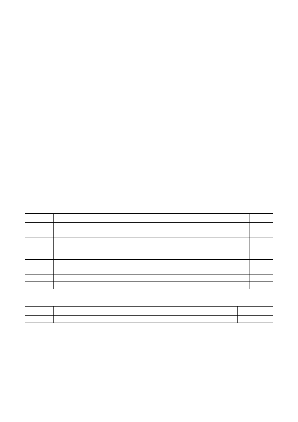
BLOCK DIAGRAM
TC1
handbook, full pagewidth
D1B
D1A
S1B
S1A
D2
S2
TC1
689
16
15
14
13
18
17
TC2
P
N
VOLTAGE TRIPLER
POWER MOS 1
POWER MOS 2
PINNING
SYMBOL PIN DESCRIPTION
NC3
NC3
V
N
V
CC
P
N
1 charge pump tank capacitor
2 charge pump tank capacitor
3 negative bias voltage
4 analog supply voltage
GND 5 ground
TC1
V
DD
TC1
TC2
TC2
V
P
N
P
N
P
6 charge pump tank capacitor
7 digital supply voltage
8 charge pump tank capacitor
9 charge pump tank capacitor
10 charge pump tank capacitor
11 positive tripler voltage
BUFI 12 buffer input
S1A 13 power MOS 1 source A
S1B 14 power MOS 1 source B
D1A 15 power MOS 1 drain A
D1B 16 power MOS 1 drain B
S2 17 power MOS 2 source
D2 18 power MOS 2 drain
R
ext
19 external resistance for V
STB 20 standby input (active HIGH)
TC2
V
N
P
10 11
STB
P
CLOCK
BUFFER
475 12
V
V
CC
Fig.1 Block diagram.
handbook, halfpage
N
NC3
20
NEGATIVE DC-DC
UBA1710M
MANAGEMENT
GND BUFI
DD
NC3
N
2
CONVERTER
POWER
NC3
NC3
TC1
TC1
TC2
TC2
V
N
P
13
MGG536
1
P
2
N
V
3
N
V
4
CC
GND
5
UBA1710M
6
N
V
7
DD
8
P
9
N
10
P
19
Fig.2 Pin configuration.
R
ext
MGG535
STB
20
19
R
ext
18
D2
17
S2
16
D1B
D1A
15
S1B
14
S1A
13
BUFI
12
V
11
P
1997 Oct 17 3
Philips Semiconductors Product specification
Modulator for GaAs power amplifiers UBA1710M
FUNCTIONAL DESCRIPTION
Power control section
Power control for GaAs PAs from the CGY20xx family is
achieved by varying the drain voltage. This is achieved
with the UBA1710M by means of the two power MOS
devices integrated on-chip. They enable separate control
of the PA output stage from the pre-amplifier stages.
They have a very low ‘on’ resistance for low drop voltage
at high RF output power.
The standard value is typically −2 V, without any external
resistor connected. The other one is a voltage tripler and
is required to supply the MOS driver. The driver is required
to raise the MOS gate voltage well above the battery
voltage in order to open the MOS switches
(‘high side’ driver).
These DC-DC converters are operated at a typical
frequency of 600 kHz supplied by an internal oscillator.
Five external capacitors with a typical value of 0.1 µF
(0603 SMD) are required to operate these converters.
The MOS devices are driven by a buffer. The buffer
amplifier, in association with power MOS, is included in a
feedback loop to exhibit a high cut-off frequency (3 MHz)
over the whole control dynamic range. This buffer allows
fast switching of the MOS in accordance with GSM power
ramping requirements.
DC-DC converters
One DC-DC converter is required to provide negative gate
biasing to the GaAs PA.
Power management
The power management disables the PA drain voltage and
prevents the PA from burnout if drain voltage is supplied
before the negative gate voltage is available.
Standby mode
An additional feature includes a standby mode, reducing
the current consumption to a maximum value of 1 µA.
LIMITING VALUES
In accordance with the Absolute Maximum Rating System (IEC 134); general operating conditions applied.
SYMBOL PARAMETER MIN. MAX. UNIT
V
CC
V
DD
V
I
analog supply voltage −0.5 +9.0 V
digital supply voltage −0.5 +9.0 V
DC input voltage
all pins (except BUFI) −0.5 +9.0 V
pin BUFI −0.5 +5.0 V
I
I
P
tot
T
stg
T
amb
DC current into any signal pin −10 +10 mA
total power dissipation − 0.65 W
storage temperature −65 +150 °C
operating ambient temperature −20 +85 °C
THERMAL CHARACTERISTICS
SYMBOL PARAMETER VALUE UNIT
R
th j-a
thermal resistance from junction to ambient 100 K/W
1997 Oct 17 4
 Loading...