

Philips UBA1707T, UBA1707TS Datasheet

INTEGRATED CIRCUITS
DATA SH EET
UBA1707
Cordless telephone, answering
machine line interface
Product specification
Supersedes data of 1998 Jun 11
File under Integrated Circuits, IC03
1999 Feb 17

Philips Semiconductors Product specification
Cordless telephone, answering machine
line interface
FEATURES
Line interface
• Low DC line voltage; operates down to 1.2 V (excluding
polarity guard)
• Voltage regulator with adjustable DC voltage
• DC mask for voltage or current regulation (CTR 21)
• Line current limitation for protection
• Electronic hook switch control input
• Transmit amplifier with:
– Symmetrical inputs
– Fixed gain
– Large signals handling capability.
• Receive amplifier with fixed gain
• Transmit and receive amplifiers AGC for line loss
compensation.
Auxiliary amplifier
• Fixed gain.
Loudspeaker channel
• Dual inputs
• Rail-to-rail output stage for single-ended load drive
• High output current capability
• Dynamic limiter to prevent distortion
• Digital volume control
• Fixed maximum gain.
General purpose switches
• Three switches with open-collector.
3-wires serial bus interface
UBA1707
• AGC:
– On/off
– Slope
–I
line current.
start
• Auxiliary amplifier mute function
• Loudspeaker channel:
– Input selection
– Volume setting
– Dynamic limiter inhibition
– Power-down mode.
• General purpose switches state
• Global power-down mode.
Supply
Operates with external supply voltage from 3.0 to 5.5 V.
APPLICATIONS
• Cordless base stations
• Answering machines
• Mains or battery-powered telephone sets.
GENERAL DESCRIPTION
The UBA1707 is a BiCMOS integrated circuit intended for
use in mains-powered telecom terminals. It performs all
speech and line interface functions, DC mask for voltage
or current regulation and electronic hook switch control.
The device includes an auxiliary amplifier, a loudspeaker
channel and general purpose switches.
Most of the characteristics are programmable via a 3-wire
serial bus interface.
Allows to control:
• DC mask (voltage or current regulation)
• Receive amplifier mute function
ORDERING INFORMATION
TYPE
NUMBER
UBA1707T SO28 plastic small outline package; 28 leads; body width 7.5 mm SOT136-1
UBA1707TS SSOP28 plastic shrink small outline package; 28 leads; body width 5.3 mm SOT341-1
1999 Feb 17 2
NAME DESCRIPTION VERSION
PACKAGE
Philips Semiconductors Product specification
Cordless telephone, answering machine
UBA1707
line interface
QUICK REFERENCE DATA
I
= 15 mA; VCC= 3.3 V; R
line
f = 1 kHz; T
=25°C; bit AGC at logic 1, all other configuration bits at logic 0; measured in test circuit of Fig.17;
amb
unless otherwise specified.
SYMBOL PARAMETER CONDITIONS MIN. TYP. MAX. UNIT
V
I
I
V
R
CC
line
CC
LN
REGC
operating voltage range 3.0 − 5.5 V
current consumption from pin V
line current operating range normal operation 11 − 140 mA
DC line voltage 2.7 3.0 3.3 V
DC mask slope in current regulation
mode
G
v(trx)
voltage gain
transmit amplifier from TXI to LN V
receive amplifier from RXI to RXO V
∆G
v(trx)
gain control range for transmit and
receive amplifiers with respect to
I
=15mA
line
G
G
v(AX)
v(LSA)
voltage gain from AXI to AXO V
voltage gain from LSAI1 or LSAI2 to
LSAO for maximum volume
∆G
v(LSA)
voltage gain adjustment range for
loudspeaker channel
∆G
v(LSA)s
voltage gain adjustment step for
loudspeaker channel
=10Ω; AGC pin connected to GND; Z
SLPE
normal operation; bit PD = 0 − 2.2 3.2 mA
CC
power-down mode; bit PD = 1 − 110 150 µA
with reduced performance 3 − 11 mA
I
> 35 mA (typical);
line
R
=1MΩ; R
LVI
bit CRC = 1
= 50 mV (RMS) 10.6 11.6 12.6 dB
TXI
= 2 mV (RMS) 36.9 37.9 38.9 dB
RXI
I
=90mA − 6.5 − dB
line
= 2 mV (RMS) 30.8 31.8 32.8 dB
AXI
V
= 8 mV (RMS);
LSAI
bits LSA1 = 1 and LSA2 = 1
bits (VOL0, VOL1, VOL2)
from (0, 0, 0) to (1, 1, 1)
VOL0 from 0 to 1 − 3 − dB
line
= 7.15 kΩ;
RGL
= 600 Ω; Z
= 619 Ω; EHI = HIGH;
SET
− 1.4 − kΩ
26.5 28 29.5 dB
− 21 − dB
1999 Feb 17 3
Philips Semiconductors Product specification
Cordless telephone, answering machine
line interface
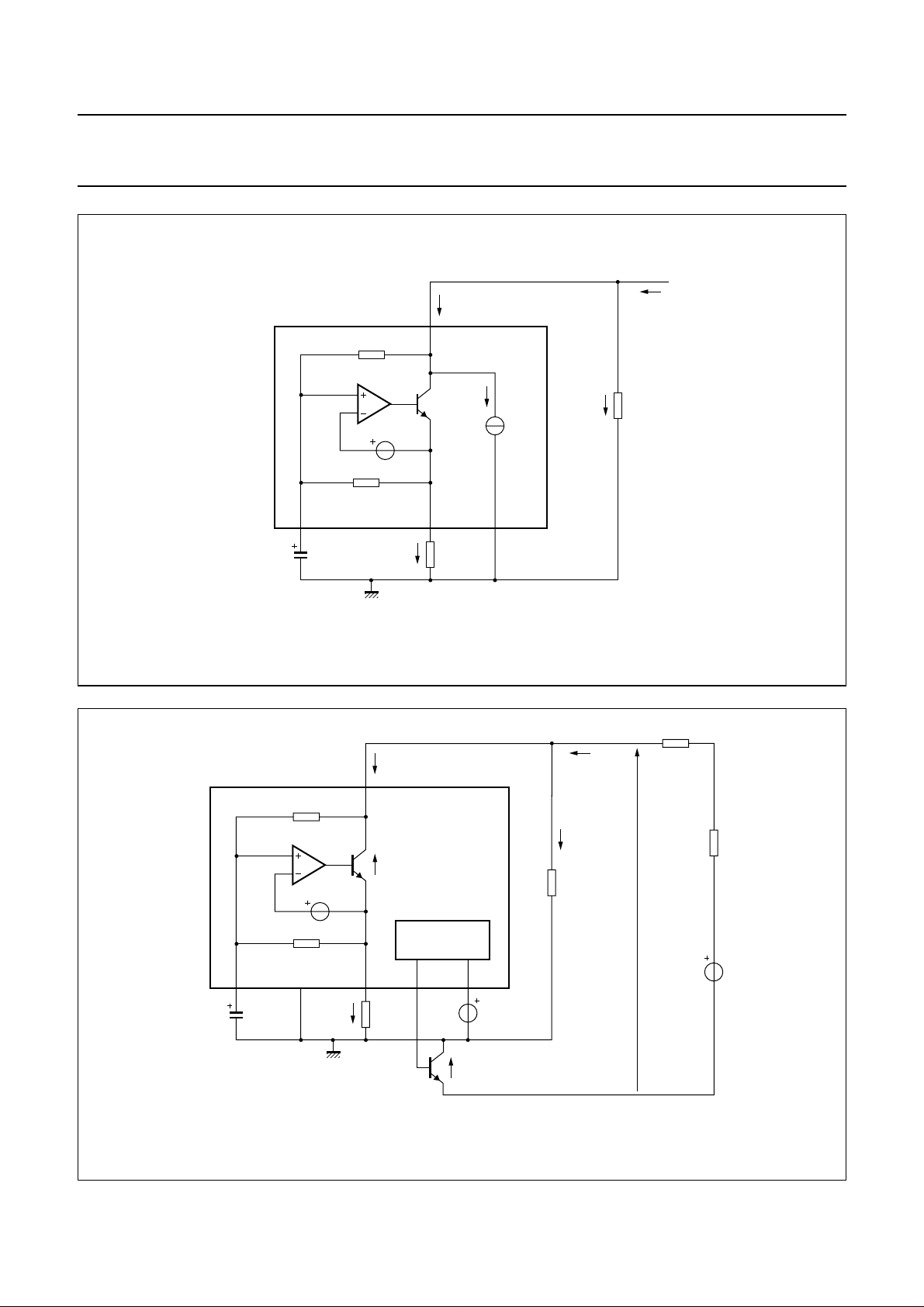
BLOCK DIAGRAM
handbook, full pagewidth
V
CC
25
RXI
10
VI
2V
d
EHI
TXI+
18
TXI−
17
AGC
9
R
RGL
RGL
5
VI
RAGC2
REG
CRC
RXM
RAGC1
EHI
600 mV
UBA1707
AGC
2
SAGC,
AGC
2V
d
300 mV
LOW VOLTAGE
PART
CURRENT
LIMITATION
200 nA
LINE INTERFACE
EHI
V
CC
SLPE
UBA1707
22
GND
8
RXO
LN
2
Z
SET
R
SLPE
SLPE
1
REG
3
C
REG
EHI
11
LCC
6
CST
7
LVI
4
V
CC
TP
TN
ON-HOOK
DARL
D
TN
SW
C
CST
R
LVI
LN +
LN −
AXI
15
26
LSAI1
27
LSAI2
LSPGND 23
Bit names are given in italics.
VI
2V
d
LSPD
VI
2V
d
19
SERIAL
INTERFACE
13 14 12
EN CLK DATA
AXM
LSA1
LSA2
SUPPLY
PD
2V
d
LOUDSPEAKER CHANNEL
0.5V
CC
LSPD
DYNAMIC LIMITER
VOLUME CONTROL
3
SWC1, SWC2,
SWC3
Fig.1 Block diagram.
AUXILIARY AMPLIFIER
V
CC
DLCI
LSPD
VOL0
TO
3
VOL2
GENERAL SWITCHES
16
24
28
21
20
19
MGK705
AXO
LSAO
DLC
SWI1
SWI2
SWI3
C
DLC
1999 Feb 17 4
Philips Semiconductors Product specification
Cordless telephone, answering machine
line interface
PINNING
SYMBOL PIN DESCRIPTION
SLPE 1 connection for slope resistor
LN 2 positive line terminal
REG 3 line voltage regulator decoupling
LVI 4 negative line voltage sense input
RGL 5 reference for current regulation mode
LCC 6 line current control output
CST 7 input for stability capacitor
RXO 8 receive amplifier output
AGC 9 automatic gain control/line loss
compensation adjustment
RXI 10 receiver amplifier input
EHI 11 electronic hook switch control input
DATA 12 serial bus data input
EN 13 programming serial bus enable input
CLK 14 serial bus clock input
AXI 15 auxiliary amplifier input
AXO 16 auxiliary amplifier output
TXI− 17 inverted transmit amplifier input
TXI+ 18 non-inverted transmit amplifier input
SWI3 19 NPN open-collector output 3
SWI2 20 NPN open-collector output 2
SWI1 21 NPN open-collector output 1
GND 22 ground reference
LSPGND 23 ground reference for the loudspeaker
amplifier
LSAO 24 loudspeaker amplifier output
V
CC
LSAI1 26 loudspeaker amplifier input 1
LSAI2 27 loudspeaker amplifier input 2
DLC 28 dynamic limiter timing adjustment
25 supply voltage
handbook, halfpage
SLPE
1
LN
2
REG
3
LVI
4
RGL
5
LCC
6
CST
7
UBA1707
8
RXO
AGC
9
RXI
10
EHI
11
DATA
12
EN
13
CLK
MGK704
Fig.2 Pin configuration.
UBA1707
DLC
28
LSAI2
27
LSAI1
26
V
25
CC
LSAO
24
23
LSPGND
GND
22
21
SWI1
SWI2
20
SWI3
19
TXI+
18
TXI−
17
AXO
16
1514
AXI
1999 Feb 17 5
Philips Semiconductors Product specification
Cordless telephone, answering machine
line interface
FUNCTIONAL DESCRIPTION
All data given in this chapter are typical values, except
when otherwise specified.
Supply (pins V
The UBA1707 must be supplied with an external stabilized
voltage source between pins V
Pins GND and LSPGND must be connected together.
Without any signal, with the loudspeaker channel enabled
at minimum volume and without any general purpose
switch selected, the internal current consumption is
2.2 mA at VCC= 3.3 V. Each selected switch
(pins SWI1, SWI2, or SWI3) increases the current
consumption by 600 µA.
The supply current can be reduced when the loudspeaker
channel is not used by switching it off (bit LSPD at logic 1).
The current consumption is then decreased by
approximately 800 µA at minimum volume.
and GND; bits PD and LSPD)
CC
and GND.
CC
UBA1707
• The automatic gain control
• The DC mask management
• The low voltage area characteristics.
In the same way, changing the value of Z
the characteristics. The IC has been optimized for
V
= 2.9 V and Z
ref
8.5
handbook, halfpage
V
ref
(V)
7.5
6.5
5.5
4.5
SET
= 619 Ω.
(1)
also affects
SET
MGK706
To drastically reduce current consumption, the UBA1707
is provided with a power-down mode controlled by bit PD.
When bit PD is at logic 1, the current consumption from
VCC becomes 110 µA. In this mode, the serial interface is
the only function which remains active.
Line interface
DC
CHARACTERISTICS (PINS LN, SLPE, REG, CST, LVI,
LCC, RGL
The IC generates a stabilized reference voltage (V
AND GND; BIT CRC)
ref
)
between pins LN and SLPE. This reference voltage is
equal to 2.9 V, is temperature compensated and can be
adjusted by means of an external resistor (RVA). It can be
increased by connecting the RVA resistor between
pins REG and SLPE (see Fig.3).
The voltage at pin REG is used by the internal regulator to
generate the stabilized reference voltage and is decoupled
by a capacitor (C
) which is connected to GND. This
REG
capacitor, converted into an equivalent inductance
(see Section “Set impedance”) realizes the set impedance
conversion from its DC value (R
(Z
in the audio-frequency range). Figure 4 illustrates
SET
) to its AC value
SLPE
the reference voltage supply configuration. As can be seen
from Fig.4, part of the line current flows into the Z
SET
impedance network and is not sensed by the UBA1707.
Therefore using the RVA resistor to change value of the
reference voltage will also modify all parameters related to
the line current such as:
3.5
2.5
3
10
(1) Influence of RVA on V
(2) V
without influence of RVA.
ref
(2)
4
10
.
ref
5
10
RVA (Ω)
6
10
Fig.3 Reference voltage adjustment with RVA.
The IC regulates the line voltage at pin LN which can be
calculated as follows:
V
V
LN
refRSLPEISLPE
I
SLPEIlineIZSET
×+=
I* I
–≅––=
lineIZSET
Where:
I
= line current
line
I
= current flowing through Z
ZSET
SET
I* = current consumed between LN and GND
(approximately 100 µA).
The preferred value for R
is 10 Ω. Changing R
SLPE
SLPE
will
affect more than the DC characteristics; it also influences
the transmit gain, the gain control characteristics, the
sidetone level and the maximum output swing on the line.
However, for compliance with CTR 21 8.66 Ω is the best
value for R
SLPE
.
1999 Feb 17 6
Philips Semiconductors Product specification
Cordless telephone, answering machine
line interface
handbook, full pagewidth
R
p
35 kΩ
V
R
d
4 kΩ
REG GNDSLPE
C
REG
4.7 µF
I
SLPE
LN
d
R
10 Ω
I
LN
UBA1707
SLPE
UBA1707
LN+
I
line
*I
I
ZSET
MGK707
Z
SET
619 Ω
handbook, full pagewidth
Fig.4 Reference voltage supply configuration.
I
LN
R
p
35 kΩ
V
R
d
4 kΩ
REG GND LCC EHISLPE
C
REG
4.7 µF
I
SLPE
LN
V
d
R
SLPE
10 Ω
UBA1707
ref
HOOK SWITCH
MANAGEMENT
TN
SW
V
CE
V
EHI
(TNSW)
I
line
I
ZSET
Z
SET
619 Ω
LN+
LN−
Z
line
R
exch
V
line
V
exch
MGK708
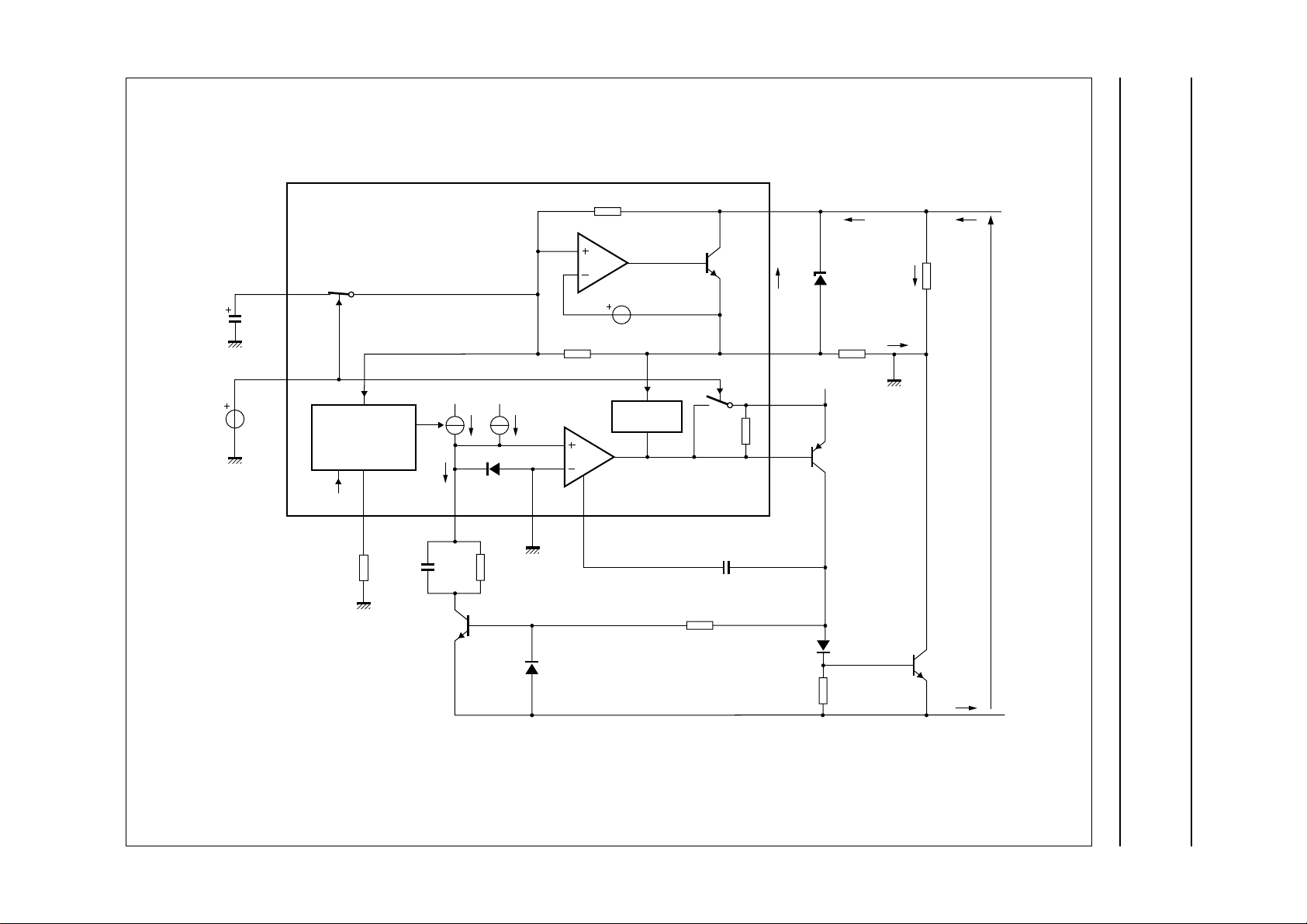
Fig.5 Line current settling simplified configuration.
1999 Feb 17 7

Philips Semiconductors Product specification
Cordless telephone, answering machine
line interface
The DC line current flowing into the set is determined by
the exchange supply voltage (V
resistance (R
(R
) and the set (R
line
), the DC resistors of the telephone line
exch
), the reference voltage (V
SET
the voltage introduced by the transistor (TNSW) used as
line interrupter (see Fig.5). With a line current below I
(8 mA with Z
(V
) is automatically adjusted to a lower value. This
ref
= 619 Ω), the internal reference voltage
SET
means that more sets can operate in parallel with DC line
voltages (excluding the polarity guard) down to 1.2 V.
At line current below I
, the circuit has limited transmit
low
and receive levels. This is called the low voltage area.
Figure 6 shows in more details how the UBA1707, in
association with some external components, manages the
line interrupter (TNSWexternal transistor).
In on-hook conditions (voltage at pin EHI is LOW), the
voltage at pin LCC is pulled-up to the supply voltage level
(VCC) to turn off the TP
of the R
resistor, the TNSWand TN
PLD
are switched off. The TN
the R
resistor from the LN− line terminal in order to
LVI
transistor. As a result, because
DARL
ON-HOOK
guarantee a high on-hook impedance.
), the feeding bridge
exch
ref
ON-HOOK
transistors
transistor disconnects
) and
low
UBA1707
In off-hook conditions (voltage at pin EHI is HIGH), an
operational amplifier drives (at pin LCC) the base of
TP
association with TNSW. The line current flows through
TNSW transistor. The TN
deep saturation. A virtual ground is created at pin LVI
because of the operational amplifier. A DC current (I
sourced from pin LVI into the R
generate a voltage source. Thus the voltage between pin
GND and the negative line terminal (LN−) becomes:
VCE (TNSW)=R
The voltage V
can be calculated as follows:
V
Where:
which forms a current amplifier structure in
DARL
transistor is forced into
resistor in order to
LVI
(TN
ON-HOOK
− I
)+VCE(TNSW)
ZSET
SET
× I
LVI
between the line terminals LN+ and LN−
line
≅ V
line
ref+RSLPE
I
= line current
line
I
= current flowing through Z
ZSET
× (I
ON-HOOK
LVI+VCE
line
) is
LVI
) ≅ R
LVI
× I
LVI
.
1999 Feb 17 8
This text is here in white to force landscape pages to be rotated correctly when browsing through the pdf in the Acrobat reader.This text is here in
a
_white to force landscape pages to be rotated correctly when browsing through the pdf in the Acrobat reader.This text is here inThis text is here in
white to force landscape pages to be rotated correctly when browsing through the pdf in the Acrobat reader. white to force landscape pages to be ...
1999 Feb 17 9
UBA1707
ndbook, full pagewidth
R
p
35 kΩ
LN
I
LN
I
line
LN+
Philips Semiconductors Product specification
Cordless telephone, answering machine
line interface
C
REG
4.7 µF
V
EHI
REG
EHI
CURRENT
REGULATION
MODE
MANAGEMENT
CRC
R
RGL
7.15 kΩ
TN
I
LVI
C
470 pF
ON-HOOK
LVI
R
LVI
1 MΩ
R
4 kΩ
I
LVIV
200 nA
GNDLVIRGL CST
D
PROT
d
V
d
CURRENT
LIMITATION
R
ON-HOOK
100 kΩ
R
PLU
150 kΩ
C
CST
22 pF
V
SLPE
LCC
D
R
20 kΩ
ref
SW
PLD
I
SLPE
10 Ω
DARL
ZSET
I
SLPE
8.2 V
R
V
CC
TP
Z
619 Ω
TN
SET
SW
I
line
MGK709
V
line
LN−
UBA1707
Bit names are given in italics.
Fig.6 Line interrupter management and DC mask regulation configuration.
Philips Semiconductors Product specification
Cordless telephone, answering machine
line interface
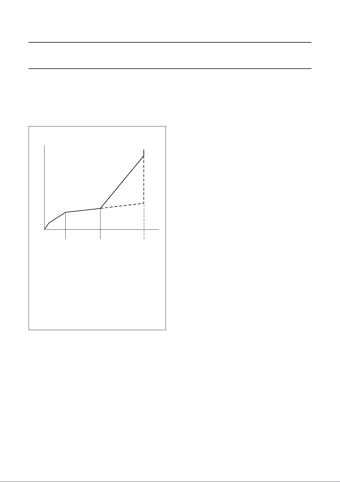
The UBA1707 offers the possibility to choose two kinds of
regulations for the DC characteristic between the line
terminals LN+ and LN− (see Fig.7):
• Voltage regulation mode
• Current regulation mode.
handbook, halfpage
V
line
I
prot
RGL
I
line
(4)
MGK710
) in
(1) (2) (3)
I
low
(1) Low voltage area.
(2) Small slope (determined by R
(3) Small slope (dashed line; determined by R
regulation mode.
High slope (full line; determined by R
current regulation mode.
(4) Current limitation.
I
knee
SLPE
).
) in voltage
SLPE
, R
LVI
and R
SLPE
Fig.7 General form of the DC mask as a function
of regulation mode.
UBA1707
Therefore VCE(TNSW) ≅ R
application (see Fig.18).
The slope ∆V
R
≅ R
REGV
line
SLPE.
/∆I
of the V
line
Current regulation mode
In current regulation mode (bit CRC at logic 1), when the
line current is lower than I
= 619 Ω), VCE(TNSW) is fixed by means of a 200 nA
Z
SET
DC constant current I
LVIV
line current is higher than 35 mA, an additional current
(proportional to the line current) flows through R
result, TN
the line current. V
()R
V
CETNSW
works as a DC voltage source increasing with
SW
(TNSW) can be calculated as follows:
CE
×≅
LVI
Where:
I
= line current
line
R
= resistor connected at pin RGL.
RGL
/∆I
The slope ∆V
line
of the V
line
determined by the ratio of resistors connected at
pins SLPE, LVI and RGL, and can be calculated as
follows: in
R
REGCRSLPERLVI
typical application (see Fig.18).
Current limitation
Whatever the selected mode is, the line current is limited
to approximately 145 mA. This current is sensed on SLPE,
for this purpose the external zener diode must be
connected between pins LN and SLPE. The speech
function no longer operates in this condition.
× I
LVI
knee
= 200 mV in typical
LVIV
, I
characteristic is
line
line
= 35 mA (with
flowing through R
R
SLPE
--------------- R
RGL
I
–()I
lineIknee
, I
characteristic is
line
line
R
SLPE
--------------- R
RGL
. When the
LVI
+×
1400 Ω=×+≅
LVI
LVIV
. As a
The regulation mode is selected by the bit CRC via the
serial interface.
The DC mask regulation is realised by adjusting the DC
voltage V
(TNSW) between pin GND and line terminal
CE
LN− as a function of the line current.
Voltage regulation mode
In voltage regulation mode (bit CRC at logic 0),
VCE(TNSW) voltage is fixed by means of a 200 nA DC
constant current I
flowing through R
LVIV
LVI
.
1999 Feb 17 10
E
LECTRONIC HOOK SWITCH CONTROL (PIN EHI)
The electronic hook switch input (EHI) controls the state of
TP
LOW, TP
pulled up to supply voltage (VCC). TNSWand TN
transistor. When the voltage applied at pin EHI is
DARL
transistor is turned off. Voltage at pin LCC is
DARL
ON-HOOK
transistors are also turned off by means of a pull-down
resistor (R
HIGH, TP
). When the voltage applied at pin EHI is
PLD
transistor is driven by the operational
DARL
amplifier at pin LCC and the regulation mode selected is
operating. An internal 165 kΩ pull-up resistor is connected
between pins LCC and VCC.
Philips Semiconductors Product specification
Cordless telephone, answering machine
line interface
The EHI input can also be used for pulse dialling or
register recall (timed loop break). During line breaks
(voltage at pin EHI is LOW or open-circuit), the voltage
regulator is switched off and the capacitor at pin REG is
internally disconnected to prevent its discharge. As a
result, the voltage stabilizer will have negligible switch-on
delay after line interruptions. This minimizes the
contribution of the IC to the current waveform during pulse
dialling or register recall.
When the UBA1707 is in power-down mode (bit PD at
logic 1), the TP
whatever the voltage applied at pin EHI.
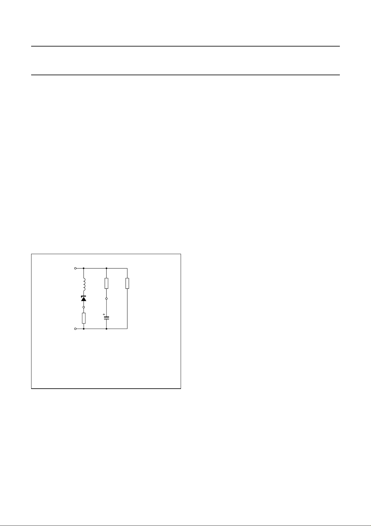
S
ET IMPEDANCE
In the audio frequency range, the dynamic impedance
between pins LN and GND (illustrated in Fig.8) is mainly
determined by the Z
The impedance introduced by the external TNSW transistor
connected between pin GND and the negative line
terminal (LN−) is negligible.
handbook, halfpage
transistor is forced to be turned off
DARL
impedance.
SET
LN
Z
L
EQ
R
P
SET
619 Ω
UBA1707
TRANSMIT AMPLIFIER (PINS TXI+ AND TXI−)
The UBA1707 has symmetrical transmit inputs TXI+ and
TXI−. The input impedance between pins TXI+ or TXI− and
GND is 21 kΩ. The voltage gain from pins TXI+ or TXI− to
pin LN is set at 11.6 dB with 600 Ω line load (Z
619 Ω set impedance. The inputs are biased at
2 × Vd≅ 1.4 V, with Vd representing the diode voltage.
Automatic gain control is provided on this amplifier for line
loss compensation.
R
ECEIVE AMPLIFIER (PINS RXI AND RXO; BIT RXM)
The receive amplifier (see Fig.9) has one input (RXI) and
one output (RXO). The input impedance between pins
RXI and GND is 21 kΩ. The rail-to-rail output stage is
designed to drive a 500 µA peak current. The output
impedance at pin RXO is approximately 100 Ω.
The voltage gain from pin RXI to pin RXO is set at 37.9 dB.
This gain value compensates typically the attenuation of
the anti-sidetone network (see Fig.10). The output as well
as the input are biased at 2 × Vd≅ 1.4 V. Automatic gain
control is provided on this amplifier for line loss
compensation. This amplifier can be muted by activating
the receive mute function (bit RXM at logic 1).
line
) and
V
SLPE
R
10 Ω
GND
Leq=C
RP= internal resistance = 35 kΩ.
REG
× R
SLPE
× R
P
ref
SLPE
REG
C
REG
4.7 µF
MGL215
Fig.8 Equivalent impedance between
LN and GND.
1999 Feb 17 11
 Loading...