

Philips UBA1706TS Datasheet

INTEGRATED CIRCUITS
DATA SH EET
UBA1706
Cordless telephone line interface
Objective specification
Supersedes data of 1999 Mar 08
File under Integrated Circuits, IC17
1999 Jun 04

Philips Semiconductors Objective specification
Cordless telephone line interface UBA1706
FEATURES
Line interface
• Low DC line voltage; operates down to 1.2 V (excluding
polarity guard)
• Voltage regulator with adjustable DC voltage
• DC mask for voltage or current regulation (CTR21)
• Line current limitation for protection
• Electronic hook switch control input
• Transmit amplifier with:
– Symmetrical inputs
– Fixed gain
– Large signal handling capability.
• Receive amplifier with fixed gain
• Transmit and receive amplifiers Automatic Gain Control
(AGC) for line loss compensation.
General purpose switches
Two switches with open-collector.
3-wire serial bus interface
APPLICATIONS
• Cordless base stations
• Mains or battery-powered telephone sets.
GENERAL DESCRIPTION
The UBA1706 is a BiCMOS integrated circuit intended for
use in mains-powered telecom terminals. It performs all
speech and line interface functions, DC mask for voltage
or current regulation and electronic hook switch control.
The device also includes general purpose switches.
Most of the characteristics are programmable via a 3-wire
serial bus interface.
Allows control of:
• DC mask (voltage or current regulation)
• Receive amplifier mute function
• AGC:
– On/off
– Slope
–I
line current.
start
• The state of the general purpose switches
• Global power-down mode.
Supply
Operates with external supply voltage from 3.0 to 5.5 V.
ORDERING INFORMATION
TYPE
NUMBER
UBA1706TS SSOP24 plastic shrink small outline package; 24 leads; body width 5.3 mm SOT340-1
NAME DESCRIPTION VERSION
PACKAGE
1999 Jun 04 2
Philips Semiconductors Objective specification
Cordless telephone line interface UBA1706
QUICK REFERENCE DATA
= 15 mA; VCC= 3.3 V; R
I
line
f = 1 kHz; T
=25°C; bit AGC at logic 1, all other configuration bits at logic 0; measured in the test circuit of Fig.14;
amb
unless otherwise specified.
SYMBOL PARAMETER CONDITIONS MIN. TYP. MAX. UNIT
V
I
I
V
R
CC
line
CC
LN
REGC
supply voltage 3.0 − 5.5 V
current consumption from pin V
line current operating range normal operation 11 − 140 mA
DC line voltage 2.7 3.0 3.3 V
DC mask slope in current regulation
mode
G
v(trx)
voltage gain
transmit amplifier from TXI to LN V
receive amplifier from RXI to RXO V
∆G
v(trx)
gain control range for transmit and
receive amplifiers with respect to
I
=15mA
line
=10Ω; AGC pin connected to GND; Z
SLPE
normal operation; bit PD = 0 − 2.2 3.2 mA
CC
power-down mode; bit PD = 1 − 110 150 µA
with reduced performance 3 − 11 mA
I
> 35 mA (typical);
line
R
=1MΩ; R
LVI
bit CRC = 1
= 50 mV (RMS) 10.6 11.6 12.6 dB
TXI
= 2 mV (RMS) 36.9 37.9 38.9 dB
RXI
I
=90mA − 6.5 − dB
line
line
= 7.15 kΩ;
RGL
= 600 Ω; Z
= 619 Ω; EHI = HIGH;
SET
− 1.4 − kΩ
1999 Jun 04 3
Philips Semiconductors Objective specification
Cordless telephone line interface UBA1706
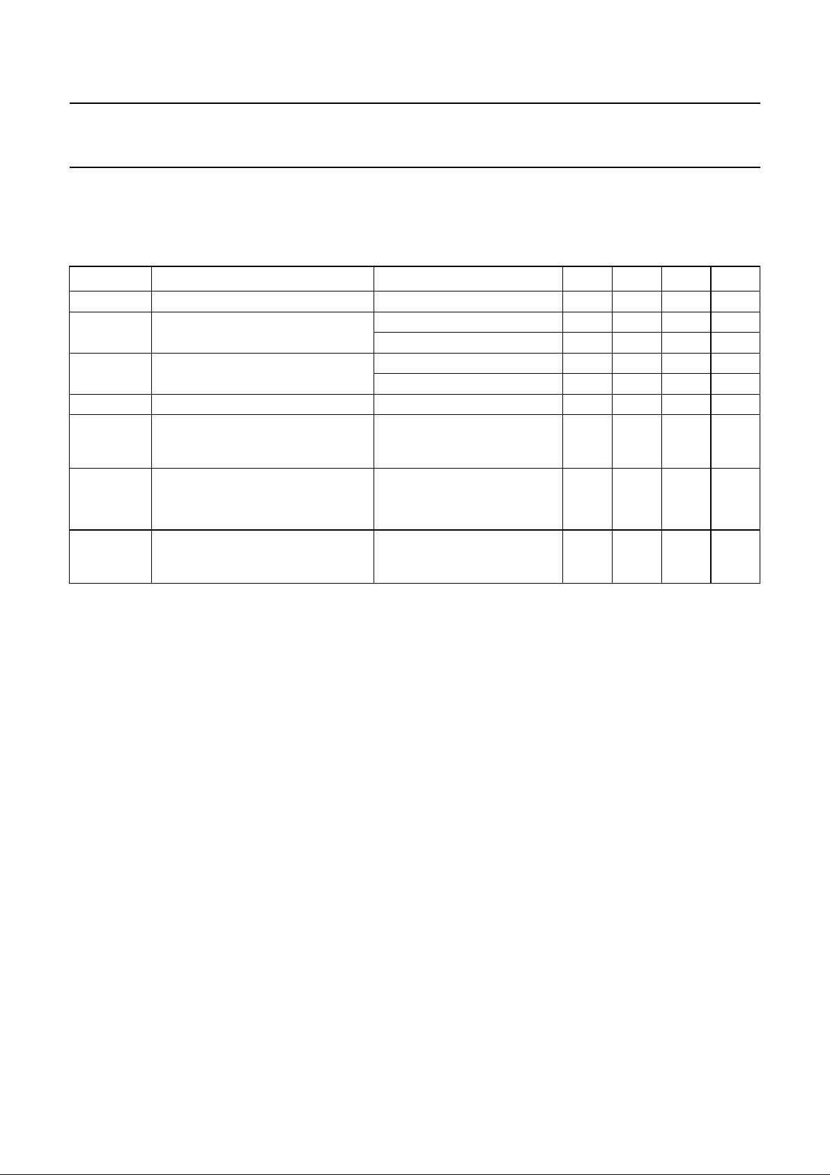
BLOCK DIAGRAM
handbook, full pagewidth
R
RGL
V
RXI
TXI+
TXI−
AGC
RGL
19
CC
21
9
15
14
8
4
RX PREAMP
2V
d
EHI
TX PREAMP
RAGC2
REG
CRC
RXM
VI
VI
RAGC1
EHI
600 mV
UBA1706
AGC
2
2V
LOW VOLTAGE
SAGC,
AGC
d
300 mV
PART
CURRENT
LIMITATION
SWITCH DRIVER
PROTECTION
200 nA
LINE INTERFACE
LINE
INTERFACE
EHI
V
CC
SLPE
GND
7
RXO
LN
1
Z
SET
R
SLPE
SLPE
24
REG
2
10
5
6
3
EHI
LCC
CST
LVI
C
REG
V
CC
TP
TN
ON-HOOK
DARL
D
TN
SW
C
CST
R
LVI
16, 20, 22, 23
n.c.
9
SERIAL
INTERFACE
12 13 11
EN CLK DATA
SUPPLY
PD
2
SWC1, SWC2
Bit names are given in italics.
Fig.1 Block diagram.
1999 Jun 04 4
GENERAL SWITCHES
MBL039
SWI1
18
SWI2
17
Philips Semiconductors Objective specification
Cordless telephone line interface UBA1706
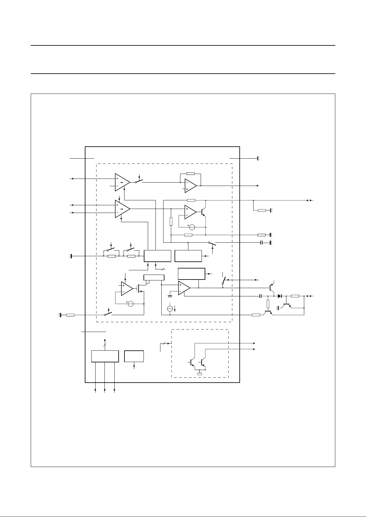
PINNING
SYMBOL PIN DESCRIPTION
LN 1 positive line terminal
REG 2 line voltage regulator decoupling
LVI 3 negative line voltage sense input
RGL 4 reference for current regulation mode
LCC 5 line current control output
CST 6 input for stability capacitor
RXO 7 receive amplifier output
AGC 8 automatic gain control/line loss
compensation adjustment
RXI 9 receiver amplifier input
EHI 10 electronic hook switch control input
DATA 11 serial bus data input
EN 12 programming serial bus enable input
CLK 13 serial bus clock input
TXI− 14 inverted transmit amplifier input
TXI+ 15 non-inverted transmit amplifier input
n.c. 16 not connected
SWI2 17 NPN open-collector output 2
SWI1 18 NPN open-collector output 1
GND 19 ground reference
n.c. 20 not connected
V
CC
21 supply voltage
n.c. 22 not connected
n.c. 23 not connected
SLPE 24 connection for slope resistor
handbook, halfpage
1
LN
2
REG
3
LVI
4
RGL
5
LCC
6
CST
UBA1706
7
RXO
8
AGC
9
RXI
10
EHI
11
DATA
12
EN
FCA031
Fig.2 Pin configuration.
24
SLPE
23
n.c.
22
n.c.
21
V
CC
20
n.c.
19
GND
18
SW1
17
SW2
16
n.c.
15
TXI+
14
TXI-
13
CLK
1999 Jun 04 5
Philips Semiconductors Objective specification
Cordless telephone line interface UBA1706
FUNCTIONAL DESCRIPTION
All data given in this chapter consists of typical values,
except when otherwise specified.
Supply (pins V
and GND; bit PD)
CC
The UBA1706 must be supplied with an external stabilized
voltage source across pins V
and GND.
CC
Without any signal and without any general purpose switch
selected, the internal current consumption is 2.2 mA at
VCC= 3.3 V. Each selected switch (pins SWI1 or SWI2)
increases the current consumption by 600 µA.
To drastically reduce current consumption, the UBA1706
is provided with a power-down mode controlled by bit PD.
When bit PD is at logic 1, the current consumption from
VCC becomes 110 µA. In the power-down mode, the serial
interface is the only function which remains active.
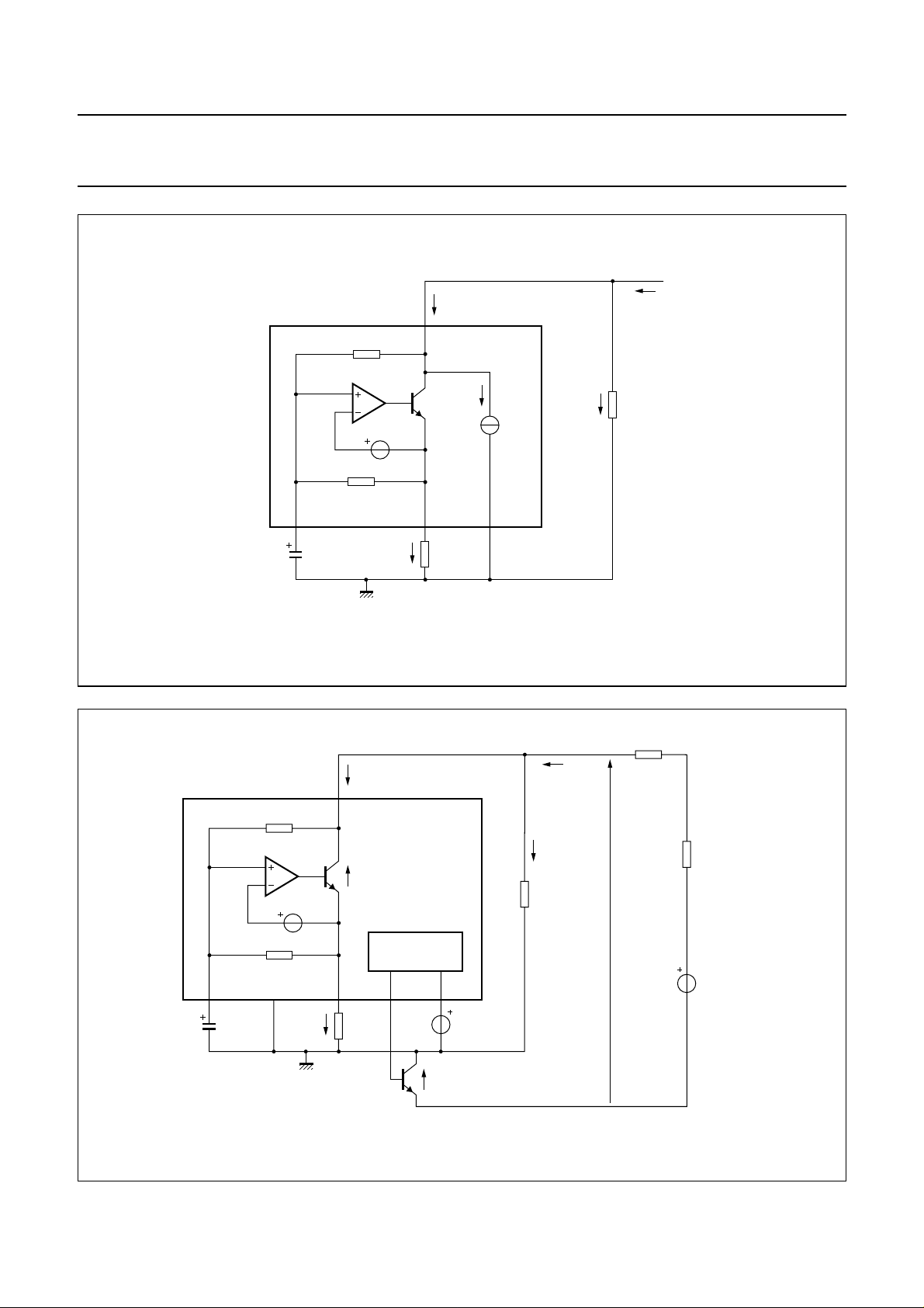
Line interface
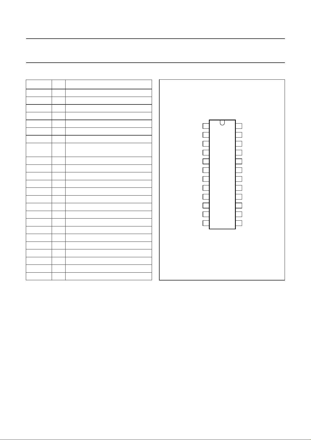
8.5
handbook, halfpage
V
ref
(V)
7.5
6.5
5.5
4.5
3.5
2.5
3
10
(1)
(2)
4
10
5
10
MGK706
RVA (Ω)
6
10
CHARACTERISTICS (PINS LN, SLPE, REG, CST, LVI,
DC
LCC, RGL
The IC generates a stabilized reference voltage (V
AND GND; BIT CRC)
ref
)
across pins LN and SLPE. This reference voltage is equal
to 2.9 V, is temperature compensated and can be adjusted
by means of an external resistor (RVA). The reference
voltage can be increased by connecting the RVA resistor
between pins REG and SLPE (see Fig.3).
The voltage at pin REG is used by the internal regulator to
generate the stabilized reference voltage and is decoupled
by a capacitor (C
) which is connected to GND. This
REG
capacitor, converted to an equivalent inductance
(see Section “Set impedance”) realizes the set impedance
conversion from its DC value (R
(Z
in the audio frequency range). Figure 4 illustrates
SET
) to its AC value
SLPE
the reference voltage supply configuration. As can be seen
from Fig.4, part of the line current flows into the Z
SET
impedance network and is not sensed by the UBA1706.
Therefore, using the RVA resistor to change the value of
the reference voltage will also modify all parameters
related to the line current such as:
• The AGC
• The DC mask management
• The low voltage area characteristics.
(1) Influence of RVA on V
(2) V
without influence of RVA.
ref
.
ref
Fig.3 Reference voltage adjustment with RVA.
The IC regulates the line voltage at pin LN, which can be
calculated as follows:
V
I
V
LN
SLPEIlineIZSET
refRSLPEISLPE
×+=
I* I
–≅––=
lineIZSET
Where:
= line current
I
line
I
= current flowing through Z
ZSET
SET
I* = current consumed between LN and GND
(approximately 100 µA).
The preferred value for R
is 10 Ω. Changing R
SLPE
SLPE
will
affect more than the DC characteristics; it also influences
the transmit gain, the gain control characteristics, the
sidetone level and the maximum output swing on the line.
Nevertheless, for compliance with CTR21, 8.66 Ω is the
optimum value for R
SLPE
.
In the same way, changing the value of Z
also affects
SET
the characteristics. The IC has been optimized for
V
= 2.9 V and Z
ref
SET
= 619 Ω.
1999 Jun 04 6
Philips Semiconductors Objective specification
Cordless telephone line interface UBA1706
handbook, full pagewidth
I
LN
R
p
35 kΩ
V
R
d
4 kΩ
REG GNDSLPE
C
REG
4.7 µF
I
SLPE
LN
UBA1706
*I
d
R
SLPE
10 Ω
I
ZSET
Fig.4 Reference voltage supply configuration.
FCA032
I
line
Z
SET
619 Ω
LN+
handbook, full pagewidth
I
LN
R
p
35 kΩ
V
R
d
4 kΩ
REG GND LCC EHISLPE
C
REG
4.7 µF
I
SLPE
LN
V
d
R
SLPE
10 Ω
Fig.5 Line current settling simplified configuration.
UBA1706
ref
HOOK SWITCH
MANAGEMENT
TN
SW
V
CE
V
EHI
(TNSW)
I
line
I
ZSET
Z
SET
619 Ω
LN+
LN−
Z
line
R
exch
V
line
V
exch
FCA033
1999 Jun 04 7

Philips Semiconductors Objective specification
Cordless telephone line interface UBA1706
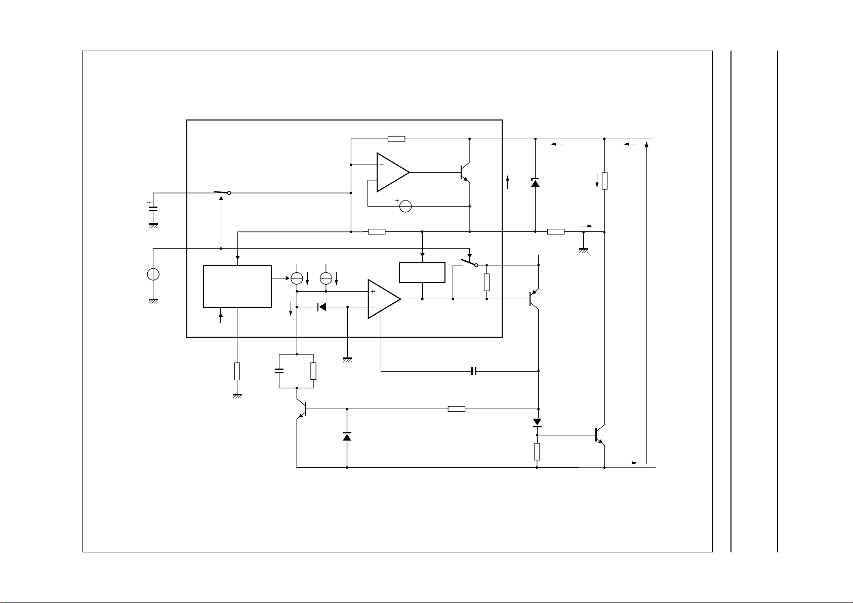
The DC line current flowing into the set is determined by
the exchange supply voltage (V
resistance (R
(R
) and the set (R
line
), the DC resistors of the telephone line
exch
), the reference voltage (V
SET
), the feeding bridge
exch
ref
) and
the voltage introduced by the transistor (TNSW) used as
line interrupter (see Fig.5).
With a line current below I
internal reference voltage (V
(8 mA with Z
low
) is automatically adjusted
ref
SET
= 619 Ω), the
to a lower value. This means that several sets can operate
in parallel with DC line voltages (excluding the polarity
guard) down to 1.2 V. With a line current below I
low
, the
circuit has limited transmit and receive levels. This is called
the low voltage area.
Figure 6 shows in more detail how the UBA1706, in
association with some external components, manages the
line interrupter (TNSWexternal transistor).
In on-hook conditions (voltage at pin EHI is LOW), the
voltage at pin LCC is pulled up to the supply voltage level
(VCC) to turn off transistor TP
resistor RPD, transistors TNSWand TN
switched off. Transistor TN
R
from the LN− line terminal to guarantee a high
LVI
. As a result, because of
DARL
ON-HOOK
ON-HOOK
disconnects resistor
are
on-hook impedance.
In off-hook conditions (voltage at pin EHI is HIGH), an
operational amplifier drives (at pin LCC) the base of
transistor TP
, which forms a current amplifier
DARL
structure in association with TNSW. The line current flows
through transistor TNSW. Transistor TN
ON-HOOK
is forced
into deep saturation. A virtual ground is created at pin LVI
because of the operational amplifier. A DC current (I
sourced from pin LVI into the R
resistor to generate a
LVI
LVI
) is
voltage source. Thus, the voltage across pins GND and
LN− becomes:
VCE (TNSW)=R
The voltage V
× I
LVI
LVI+VCE
across line terminals LN+ and LN− can
line
(TN
ON-HOOK
) ≅ R
LVI
× I
LVI
be calculated as follows:
V
line
≅ V
ref+RSLPE
× (I
line
− I
ZSET
)+VCE(TNSW)
Where:
I
= line current
line
I
= current flowing through Z
ZSET
SET
.
1999 Jun 04 8
This text is here in white to force landscape pages to be rotated correctly when browsing through the pdf in the Acrobat reader.This text is here in
_white to force landscape pages to be rotated correctly when browsing through the pdf in the Acrobat reader.This text is here inThis text is here in
white to force landscape pages to be rotated correctly when browsing through the pdf in the Acrobat reader. white to force landscape pages to be ...
1999 Jun 04 9
R
p
35 kΩ
UBA1706
LN
I
LN
I
line
Philips Semiconductors Objective specification
Cordless telephone line interface UBA1706
LN+
C
REG
4.7 µF
V
EHI
REG
EHI
CURRENT
REGULATION
MODE
MANAGEMENT
CRC
R
RGL
7.15 kΩ
TN
I
LVI
C
470 pF
ON-HOOK
LVI
R
LVI
1 MΩ
R
4 kΩ
I
LVIV
200 nA
GNDLVIRGL CST
D
prot
d
V
d
CURRENT
LIMITATION
R
ON-HOOK
100 kΩ
R
PLU
150 kΩ
C
CST
22 pF
V
SLPE
LCC
D
R
20 kΩ
ref
SW
PD
I
SLPE
10 Ω
DARL
ZSET
I
SLPE
8.2 V
R
V
CC
TP
Z
619 Ω
TN
SET
SW
I
line
FCA034
V
line
LN−
Bit names are given in italics.
Fig.6 Line interrupter management and DC mask regulation configuration.
handbook, full pagewidth
 Loading...