

Philips UBA1702A, UBA1702 Datasheet

INTEGRATED CIRCUITS
DATA SH EET
UBA1702; UBA1702A
Line interrupter driver and ringer
Product specification
Supersedes data of 1996 Jan 09
File under Integrated Circuits, IC03
1997 Sep 29
Philips Semiconductors Product specification
Line interrupter driver and ringer UBA1702; UBA1702A
FEATURES
Speech part
• Driver for the line interrupter that can be either a PMOST
when UBA1702 is used or a PNP when UBA1702A is
used
• Adjustable over-current protection
• Adjustable over-voltage protection for transmission
circuit
• Adjustable mute (dialling mode voltage; DMO or NSA)
• Adjustable current loop detection (hook switch status)
• Microcontroller supply
• Provision for electronic hook switch.
Ringer part
• Over-voltage protection
• Ringer frequency output for frequency discrimination
• Adjustable ringer threshold for piezo-driver enable
• Three bits ringer volume control
• Bridge-tied-load (BTL) output stage for piezo transducer
• Fast start-up microcontroller supply.
Miscellaneous
• Separated ground pins for transmission circuit interface
and control signals (e.g. for TEA1064A)
• Possibility to supply the microcontroller with an external
voltage source.
APPLICATIONS
• Telephone sets with software controlled ringer function
• Telephone sets with electronic hook switch.
GENERAL DESCRIPTION
The UBA1702; UBA1702A performs the high voltage
interface and ringer functions of the corded analog
telephone set in close cooperation with a microcontroller
and transmission circuit.
The UBA1702; UBA1702A incorporates several
protections, a driver for the line interrupter and a ringer.
Because of the practical division of functions between the
microcontroller, the transmission circuit and the UBA1702;
UBA1702A, it is possible to have a higher integration level
thereby reducing significantly the number of discrete
components in a telephone set.
ORDERING INFORMATION
TYPE NUMBER
NAME DESCRIPTION VERSION
UBA1702 DIP28 plastic dual in-line package; 28 leads (600 mil) SOT117-1
UBA1702A DIP28 plastic dual in-line package; 28 leads (600 mil) SOT117-1
UBA1702T SO28 plastic small outline package; 28 leads; body width 7.5 mm SOT136-1
UBA1702AT SO28 plastic small outline package; 28 leads; body width 7.5 mm SOT136-1
PACKAGE
1997 Sep 29 2
Philips Semiconductors Product specification
Line interrupter driver and ringer UBA1702; UBA1702A
QUICK REFERENCE DATA
Speech part: l
Ringer part: V
line and the RPI input.
SYMBOL PARAMETER CONDITIONS MIN. TYP. MAX. UNIT
Speech part
SWITCH DRIVER AND REFERENCES (PINS SDI, SDO, EHI AND DPI); UBA1702A ONLY
R
SDO
SWITCH DRIVER AND REFERENCES (PINS SDI, SDO, EHI AND DPI); UBA1702 AND UBA1702A
R
SDI-SDO
R
SDI
MUTE SWITCH AND ADJUSTABLE PROTECTION ZENER VOLTAGE (PINS MSI, MSA AND ZPA)
V
SPO(M)
V
SPO(Z)
CURRENT MANAGEMENT (PINS SPI, SPO, CDA, CLA AND CDO)
l
SPI(lim)
I
SPI(det)
MICROCONTROLLER SUPPLY (V
V
DD
Ringer part
= 20 mA; DPI = LOW; T
line
= 45 V; f = 25 Hz; using an RC combination of 2.2 kΩ and 820 nF and a diode bridge between the
line(rms)
resistance between pins SDO and V
resistance between pins SDI and SDO V
resistance between pins SDI and V
adjustable mute voltage referenced to
V
EE
adjustable zener voltage referenced to
V
EE
current limitation (pin SPI) CLA shorted to V
=25°C; VEE= 0 V; unless otherwise specified.
amb
EE
SDI
EEVSDI
MSI = HIGH;
− V
<12V − 1.1 − MΩ
SDO
= 240 V; DPI = HIGH 5 −−MΩ
− 2.2 − kΩ
− 2.7 3 V
MSA open-circuit
MSI = LOW;
11 12 13 V
ZPA open-circuit
EE
− 120 − mA
current detection (pin SPI) CDA open-circuit 2 3 4 mA
AND V
DD
supply output voltage referenced to
V
SS
BB
)
VBB> 3.7 V; IDD= −1 mA 3.0 3.3 3.6 V
P
ROTECTION (PIN RPI)
I
RPI(max)
maximum input current 70 −−mA
RINGER THRESHOLD AND FREQUENCY DETECTION (PINS VRR,RTAAND RFO)
V
RR(th)
ringer supply threshold voltage
referenced to V
SS
RTA open-circuit − 11 − V
VOLUME CONTROL (PINS RV0, RV1 AND RV2)
∆G
s
step resolution (RV2, RV1, RV0) from
(0, 0, 0) to (1, 1, 0); note 1
∆G
ls
last step resolution (RV2, RV1, RV0) from
(1, 1, 0) to (1, 1, 1); note 2
RINGER MELODY INPUT AND PIEZO DRIVER (PINS RMI, ROA AND ROB)
V
o(max p−p)
maximum output voltage between pins
RV2=1; RV1=1; RV0=1 − 28.7 32 V
ROA and ROB (peak-to-peak value)
Notes
1. Independent of V
if greater than 10 V.
RR
2. Without piezo transducer, dependent on VRR.
1997 Sep 29 3
− 6 − dB
− 9.5 12 dB
Philips Semiconductors Product specification
Line interrupter driver and ringer UBA1702; UBA1702A
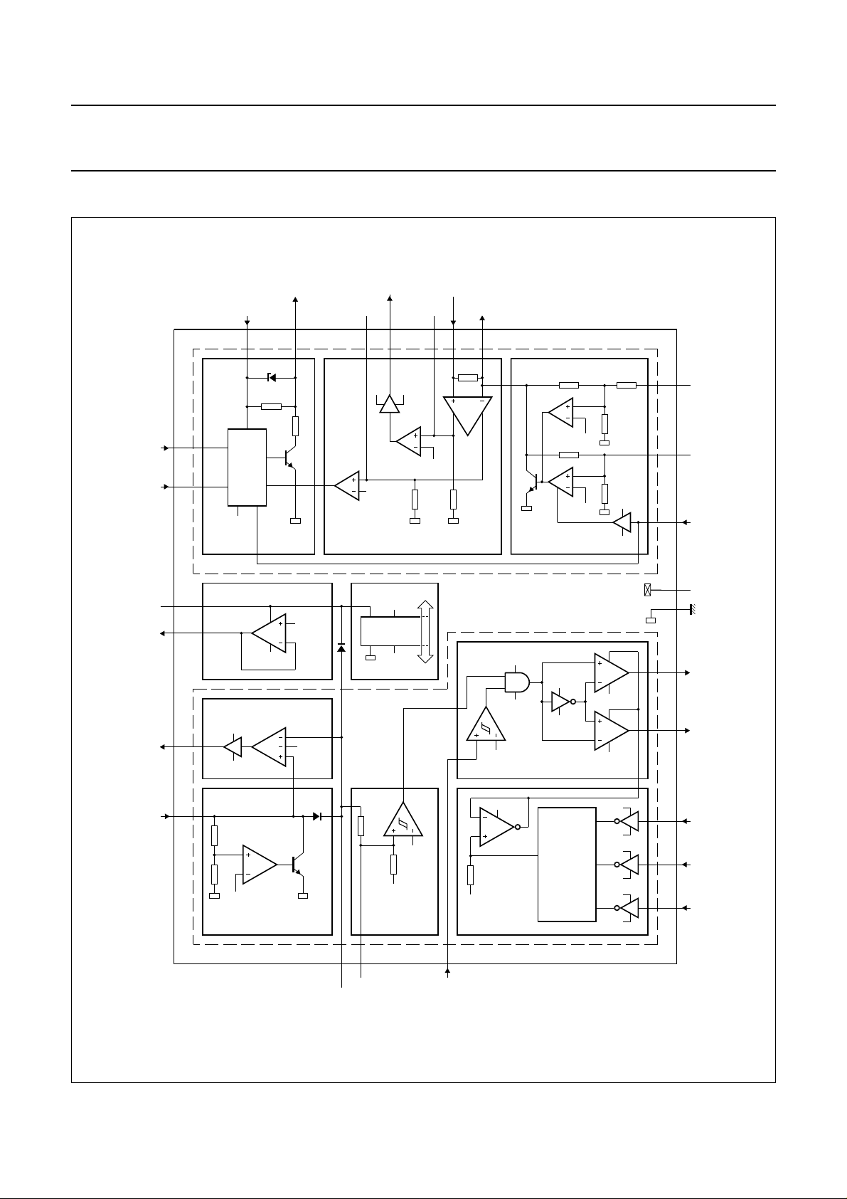
BLOCK DIAGRAM
handbook, full pagewidth
DPI
EHI
V
BB
V
DD
RFO
SDO
SDI
21
14 V
4
28
V
SS
SWITCH
DRIVER
19
18
12
SUPPLY
V
V
SS
RINGER FREQUENCY
DETECTION
V
DD
V
SS
ref
V
DD
CDO
CLA
V
V
DD
SS
S
ref
LINE CURRENT MANAGEMENT
SPO
REFERENCES
V
SS
RINGER
SPI
CDA
SENSE
S
ref
S
ref
R
ref
SPO
65262425
SPEECH
ZENER PROTECTION
S
R
MUTE SWITCH
ref
V
DD
ref
V
SS
UBA1702; UBA1702A
UBA1702T; UBA1702AT
V
RR
V
RR
V
V
SS
V
SS
1/2 V
DD
RINGER MELODY INPUT AND PIEZO DRIVER
DD
V
DD
9
ZPA
10
MSA
8
MSI
17
V
SS
7
V
EE
22
ROA
20
ROB
23
RPI
R
ref
V
11
RTA
SS
RINGER
THRESHOLD
R
ref
RINGER
PROTECTION
21
V
RR
Fig.1 Block diagram.
1997 Sep 29 4
RMI
V
RR
DIGITAL
-TO-
ANALOG
CONVERTER
V
DD
VOLUME
CONTROL
16
V
DD
V
SS
V
DD
V
SS
V
DD
V
SS
MBE184
13
RV0
14
RV1
15
RV2
Philips Semiconductors Product specification
Line interrupter driver and ringer UBA1702; UBA1702A
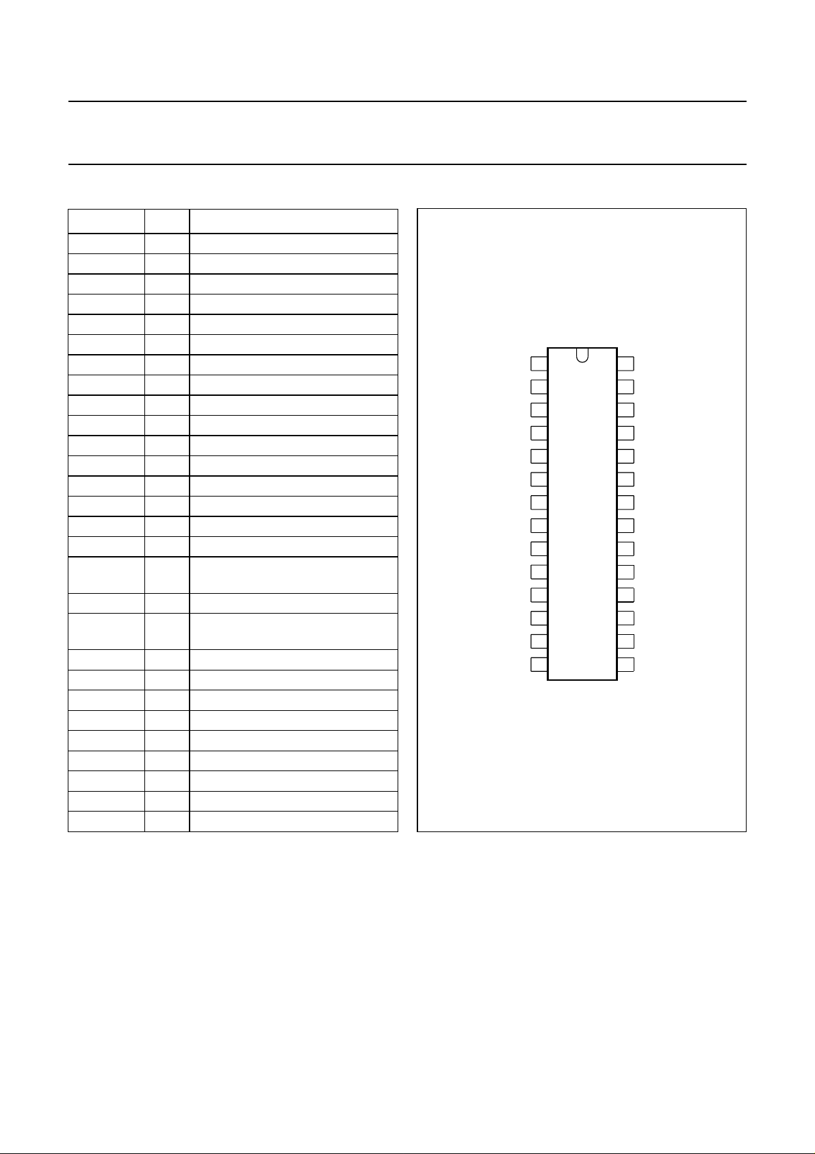
PINNING
SYMBOL PIN DESCRIPTION
SDI 1 switch driver input
SDO 2 switch driver output
n.c. 3 not connected
DPI 4 dialling pulse input
SPI 5 speech part input
SPO 6 speech part output
V
EE
7 ground for transmission circuit
MSI 8 mute switch input
ZPA 9 Zener protection adjustment input
MSA 10 mute switch adjustment input
RTA 11 ringer threshold adjustment input
RFO 12 ringer frequency output
RV0 13 ringer volume input; bit 0
RV1 14 ringer volume input; bit 1
RV2 15 ringer volume input; bit 2
RMI 16 ringer melody input
V
SS
17 ground for microcontroller and
ringer
V
DD
V
BB
18 microcontroller supply voltage
19 supply voltage from transmission
circuit
ROB 20 ringer output B
V
RR
21 ringer supply voltage
ROA 22 ringer output A
RPI 23 ringer part input
CDO 24 current detection output
CLA 25 current limitation adjustment input
CDA 26 current detection adjustment input
n.c. 27 not connected
EHI 28 electronic hook switch input
handbook, halfpage
1
SDI
2
SDO
3
n.c.
4
DPI
SPI
5
6
SPO
7
8
9
10
11
12
13
UBA1702
UBA1702T
UBA1702A
UBA1702AT
MBE183
V
EE
MSI
ZPA
MSA
RTA
RFO
RV0
RV1
Fig.2 Pin configuration.
28
EHI
27
n.c.
26
CDA
25
CLA
24
CDO
23
RPI
22
ROA
V
21
RR
20
ROB
V
19
BB
V
18
DD
V
17
SS
16
RMI
1514
RV2
1997 Sep 29 5
Philips Semiconductors Product specification
Line interrupter driver and ringer UBA1702; UBA1702A
FUNCTIONAL DESCRIPTION
The values given in this functional description are typical
values except when otherwise specified.
Speech part
The speech part consists of three blocks, the switch driver,
the line current management and the mute switch (DMO or
NSA) combined with an adjustable over-voltage (zener)
protection circuit. The reference block, which generates
reference voltages and currents, is also used in the speech
part (see Fig.1) by the mute switch block.
WITCH DRIVER (PINS SDI, SDO, EHI AND DPI)
S
UBA1702
The UBA1702 switch driver block is intended to generate
the appropriate signal to drive an external PMOST
interrupter. The source and gate of this PMOST are
respectively connected to SDI and SDO. The electronic
hook switch input (EHI) and the dialling pulse input (DPI)
signals control the state of this PMOST.
The EHI pin is provided with high voltage capability. When
the voltage applied at pin EHI is HIGH, the switch driver
block will start and generate the proper signals to switch on
the external PMOST interrupter.
When the telephone set is equipped with a mechanical
hook switch, pin EHI can be connected directly to the
switch driver input (pin SDI). For electronic hook switch
applications, the EHI pin can be driven by the
microcontroller output.
voltage applied at pin DPI is LOW, the switch driver block
turns on the external PMOST interrupter.
The external PMOST interrupter is controlled by the
voltage between the switch driver input and output
(pins SDI and SDO).
When the voltage applied at pin EHI is HIGH and the
voltage applied at pin DPI is LOW, the voltage at SDO is
pulled down to a value less than 0.2 V in order to create a
high source-gate voltage (V
) for the external PMOST.
SG
However, in order to avoid break-down of the external
PMOST, the voltage difference between SDI and SDO is
internally limited to 14 V.
When the voltage applied at pin EHI and the one applied
at pin DPI are both HIGH, pin SDO can be considered as
being connected to pin SDI via a 1.1 MΩ pull-up resistor
while the impedance between SDI and VEE becomes very
high (a few MΩ).
When the voltage applied at pin EHI is LOW, whatever the
one applied at DPI is, pin SDO can be considered as being
connected to pin SDI via a 1.1 MΩ pull-up resistor while
the impedance between SDI and VEE becomes almost
infinite.
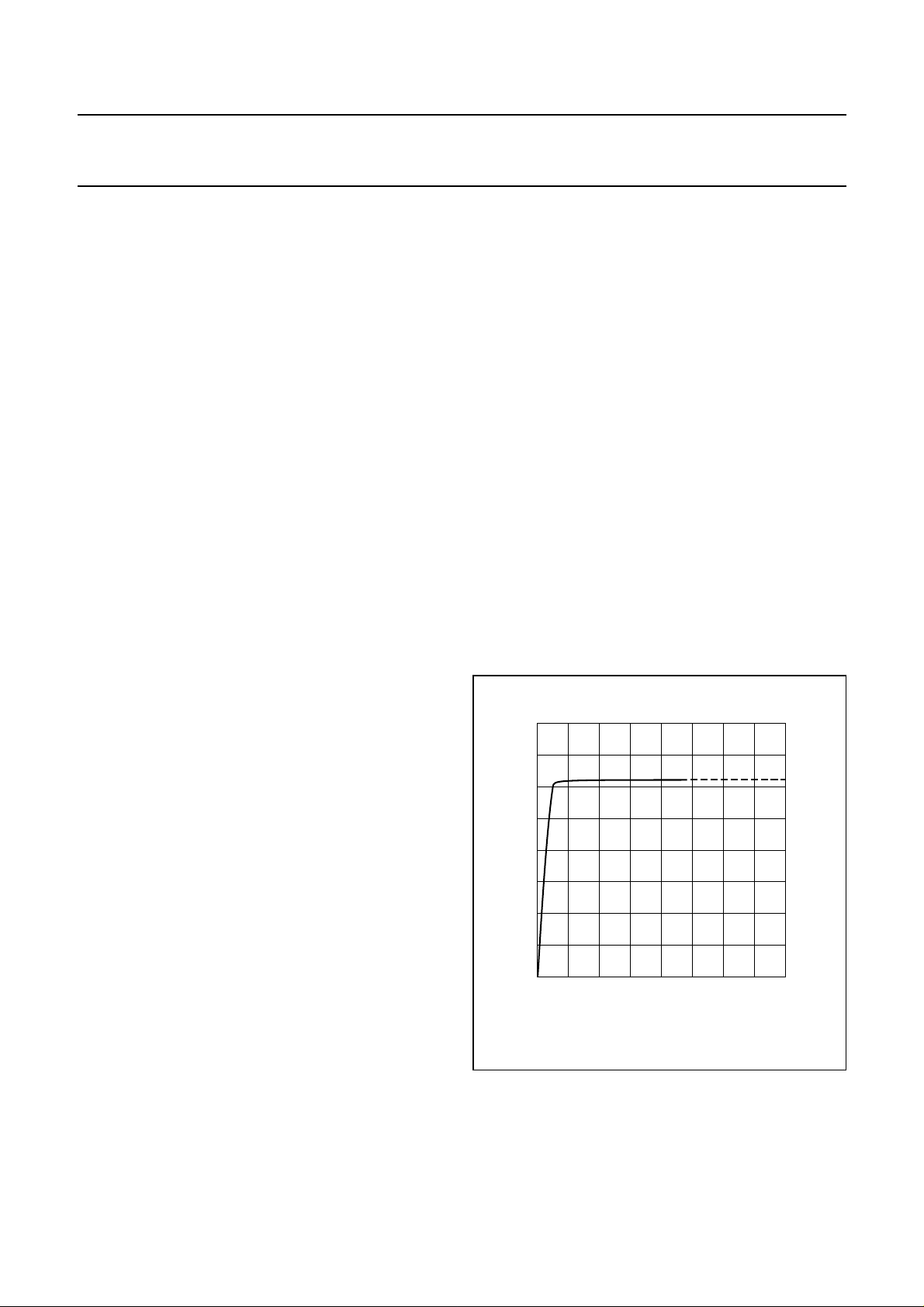
80
handbook, halfpage
I
EHI
(µA)
60
MGD178
In some special applications, the EHI pin can be current
driven. In such a case, the current available at SDO to turn
on the PMOST interrupter is approximately 10 times the
EHI input current (providing I
EHI
<2µA).
The EHI pin presents an impedance of 250 kΩ at low input
voltage. When the applied voltage at EHI goes above
approximately 30 V, the EHI input current remains
constant (see Fig.3) so that the EHI impedance increases.
The DPI is designed to switch on or off the external
PMOST interrupter (providing EHI is HIGH). When the
voltage applied at pin DPI is HIGH, the switch driver block
turns off the external PMOST interrupter. When the
1997 Sep 29 6
40
20
0
0 100 200 400
300
V
EHI
Fig.3 EHI input characteristics.
(V)

Philips Semiconductors Product specification
Line interrupter driver and ringer UBA1702; UBA1702A
UBA1702A
The UBA1702A switch driver block is intended to generate
the appropriate signal to drive an external PNP interrupter.
The emitter and base of this PNP are respectively
connected to SDI and SDO. The EHI and DPI signals
control the state of this PNP.
The EHI pin is provided with high voltage capability. When
the voltage applied at pin EHI is HIGH, the switch driver
block will start and generate the appropriate signals to
switch on the external PNP interrupter.
When the telephone set is equipped with a mechanical
hook switch, pin EHI can be connected directly to pin SDI.
For electronic hook switch applications, the EHI pin can be
driven by the microcontroller output.
The EHI pin presents an impedance of 250 kΩ at low input
voltage. When the applied voltage at EHI goes above
approximately 30 V, the EHI input current remains
constant (see Fig.3) so that the EHI impedance increases.
The DPI is designed to switch on or off the external PNP
interrupter (providing EHI is HIGH). When the voltage
applied at pin DPI is HIGH, the switch driver block turns off
the external PNP interrupter. When the voltage applied at
pin DPI is LOW, the switch driver block turns on the
external PNP interrupter.
The external PNP interrupter is controlled by the current
flowing into pin SDO.
When the voltage applied at pin EHI is HIGH and the
voltage applied at pin DPI is LOW, pin SDO can be
considered as being connected to pin V
resistor in order to create a base current for the external
PNP.
When the voltage applied at pin EHI and the one applied
at pin DPI are both HIGH, pin SDO can be considered as
being connected to pin SDI via a 1.1 MΩ pull-up resistor
while the impedance between SDI and VEE becomes very
high (a few MΩ).
via a 2.2 kΩ
EE
L
INE CURRENT MANAGEMENT
(PINS SPI, SPO, CDA, CLA AND CDO)
The line current is measured by an internal 2 Ω resistor
and a sense circuit connected between the speech part
input and output (pins SPI and SPO). The circuit delivers
information about the hook switch status at the current
detection output (pin CDO) and controls the line current
limitation.
When the SPI current exceeds a certain level (3 mA), the
sense circuit injects some image of the SPI current into an
internal resistor (see Fig.1). The created voltage becomes
higher than an internal reference (approximately 0.3 V)
and CDO goes HIGH. This current detection level can be
increased by connecting a resistor between pins CDA
(current detection adjustment) and VEE. It is also possible
to connect a capacitor between pins CDA and VEE to filter
unwanted AC components of the line current signal. Line
current interruption during pulse dialling influences the
CDO output.
When the SPI current exceeds another current level
(45 mA), the sense circuit injects some image of the SPI
current into an internal resistor (see Fig.1). The created
voltage becomes higher than an internal reference
(approximately 0.4 V) and an internal signal is generated
in order to limit the current in the external interrupter thus
resulting in a line current limitation. This line current
limitation level can be increased up to a maximum value of
120 mA by connecting a resistor between pins CLA
(current limitation adjustment) and VEE.
When a PMOST (UBA1702) is used as an interrupter, the
SPI current equals the drain or source current of the
PMOST and thus also equals the line current.
When a PNP (UBA1702A) is used as an interrupter, the
SPI current equals the collector current of the PNP and
thus differs from the line current (the PNP base current
does not flow into the SPI pin).
When the voltage applied at pin EHI is LOW, whatever the
one applied at DPI is, pin SDO can be considered as being
connected to pin SDI via a 1.1 MΩ pull-up resistor while
the impedance between SDI and VEE becomes almost
infinite.
1997 Sep 29 7

Philips Semiconductors Product specification
Line interrupter driver and ringer UBA1702; UBA1702A
MUTE SWITCH AND ZENER PROTECTION
(PINS MSI, MSA AND ZPA)
The mute switch is, in fact, a switchable and electronic
zener diode connected between the speech part output
(pin SPO) and VEE.
When the voltage applied at the mute switch input
(pin MSI) is LOW, the switch is in over-voltage protection
mode and the maximum SPO voltage is limited to 12 V.
This level can be increased or decreased by connecting a
resistor between pins ZPA (zener protection adjustment)
and VEE or ZPA and SPO respectively.
When the voltage applied at pin MSI is HIGH, the switch is
in mute mode (DMO or NSA) resulting in a SPO voltage
below 3 V. This level can be decreased by connecting a
resistor between pins MSA (mute switch adjustment) and
SPO. It should be noted that the mute switch stage is
supplied from VDD thus a minimum voltage of
approximately 2.1 V is required on VDD.
R
EFERENCE
The bias currents and voltages for the various speech
blocks are generated by the reference block which is, in
most cases, supplied from pin SPO. This block guarantees
a high AC impedance at the SPO pin operating down to a
low SPO voltage. Therefore, most speech part blocks
operate independently from VDD.
Ringer part
The ringer part consists of five blocks, the ringer
protection, the ringer threshold, the ringer frequency
detection, the volume control and the piezo driver.
The reference block which generates reference voltages
and currents is also used in the ringer part (see Fig.1).
R
INGER PROTECTION (PINS RPI AND V
RR
)
The ringer protection block converts the ringing current
into a limited voltage between the ringer part input
(pin RPI) and V
. This voltage is used (via an internal
EE
diode) to generate the ringer supply voltage VRR which is
mainly used for all ringer parts. The voltage at pin V
RR
must be filtered with a 22 µF capacitor connected between
pins VRR and VSS.
In electronic hook switch applications and also in speech
mode (see Fig.8), pin RPI is always connected to the
telephone line (through a series RC network and a diode
bridge). In order not to disturb normal speech operation, a
high AC impedance is present at pin RPI (providing the
speech level is less than 1.5 V (RMS) i.e. 5.7 dBm).
In the DMO or NSA mode (i.e. MSI is HIGH), the voltage
across RPI and V
is limited to 2.1 V. With this feature
EE
and in electronic hook switch applications, several
additional ringers can be placed in parallel without tinkling
during pulse dialling phase.
R
INGER THRESHOLD (PIN RTA)
The piezo driver is internally enabled when the voltage at
pin VRR exceeds a threshold level of 11 V. This threshold
level can be increased or decreased by connecting a
resistor between pins RTA (ringer threshold adjustment)
and V
or RTA and VRR respectively.
SS
Because of the built-in 6.5 V hysteresis, a voltage change
at pin VRR (coming from current consumption increase
when the piezo output is driven with a melody) will have no
influence on this internal enabling signal.
R
INGER FREQUENCY DETECTION (PIN RFO)
The ringer frequency detection block generates a square
wave signal at the ringer frequency output (pin RFO) with
twice the ringer signal frequency. This RFO signal can be
used by the microcontroller for frequency discrimination.
When the voltage at pin RPI drops below the voltage at
pin VDD, RFO goes LOW. Pin RFO goes HIGH when the
voltage at pin RPI exceeds the voltage at pin VRR.
This VRR− VDD hysteresis allows the frequency detection
circuit to ignore parasitic signals superimposed on the
ringing signal.
The voltage at pin EHI must be LOW to get a square wave
at pin RFO. When the voltage at pin EHI is LOW, the
voltage at pin RFO is always HIGH whatever the one at pin
RPI is.
V
OLUME CONTROL (PINS RV0, RV1 AND RV2)
The volume control input has three bits RV2, RV1 and RV0
to realize eight volume levels. The volume is controlled by
regulating the supply voltage of the piezo output stage.
The first six steps have a fixed value of 6 dB, the value of
the last step (maximum volume) is dependent on the
available voltage at pin VRR.
Default setting during start-up is (RV2 = 0, RV1 = 0,
RV0 = 0) which corresponds to minimum volume. In order
not to damage the piezo transducer, the differential output
ROA − ROB is internally limited to a value less than
32 V (p-p).
1997 Sep 29 8
 Loading...