

Philips UAA3545HL Datasheet

INTEGRATED CIRCUITS
DATA SH EET
UAA3545
Fully integrated DECT transceiver
Product specification
File under Integrated Circuits, IC17
2001 Sep 06

Philips Semiconductors Product specification
Fully integrated DECT transceiver UAA3545
FEATURES
• Economical solution for a radio in DECT cordless
telephones
• Integrated low phase noise VCO with no production
tuning required
• Fully integrated receiver with high sensitivity
• Dedicated DECT PLL synthesizer
• 3 dBm output preamplifier with an integrated switch
• 3-line serial interface bus
• Low current consumption from a 3.2 V supply
• Compatible with Philips Semiconductors baseband
chips (PCD509xx and PCD80xxx)
• Reduced number of control signals.
APPLICATIONS
• DECT cordless telephones: 1880 to 1930 MHz.
GENERAL DESCRIPTION
The UAA3545 BiCMOS device is a low power, highly
integrated circuit, for Digital Enhanced Cordless
Telecommunication (DECT) applications.
It features a fully integrated receiver, from antenna filter
output to the demodulated data output, a fully integrated
VCO, a synthesizer to implement a phase-locked loop for
DECT channel frequencies and aTXpreamplifierto drive
the external transmit power amplifier (CGY20xx series or
UAA359x series of Philips integrated circuits).
The synthesizer’s main divider is driven by the prescaler
output in the range of 1880 to 1930 MHz and is
programmed via a 3-wire serial bus. The reference divider
ratio is programmable to 4, 8, 12 or 16. Outputs of the
main and reference dividers drive a phase comparator
whereachargepumpproducesphaseerrorcurrentpulses
for integration in an external loop filter (only a passive loop
filter is necessary). The charge-pump current is set to
4 mA for fast switching.
The VCO is powered from an internally regulated voltage
source and includes integrated variable capacitance
diodesandintegratedcoils.Itstuning range is guaranteed.
The VCO and the synthesizer are switched-on one slot
before the active slot to lock the VCO to the required
channel frequency. Immediately before the active slot, the
synthesizer is switched-off to allow open loop modulation
of the VCO during transmission. When opening the loop,
frequency pulling (due to switching-off the synthesizer)
can be maintained within the DECT specification.
The device is designed to operate from a 3.2 V nominal
supply. Separate power and ground pins are provided for
thedifferentsectionsofthecircuit.Groundleadsshouldbe
short-circuited externally to prevent large currents flowing
across the die and causing damage. All VCC supplies
(V
CC(REG)
, V
CC(SYN)
, V
CC(RX)
and V
) must be at the
CC(TX)
same potential (VCC).
ORDERING INFORMATION
TYPE
NUMBER
NAME DESCRIPTION VERSION
PACKAGE
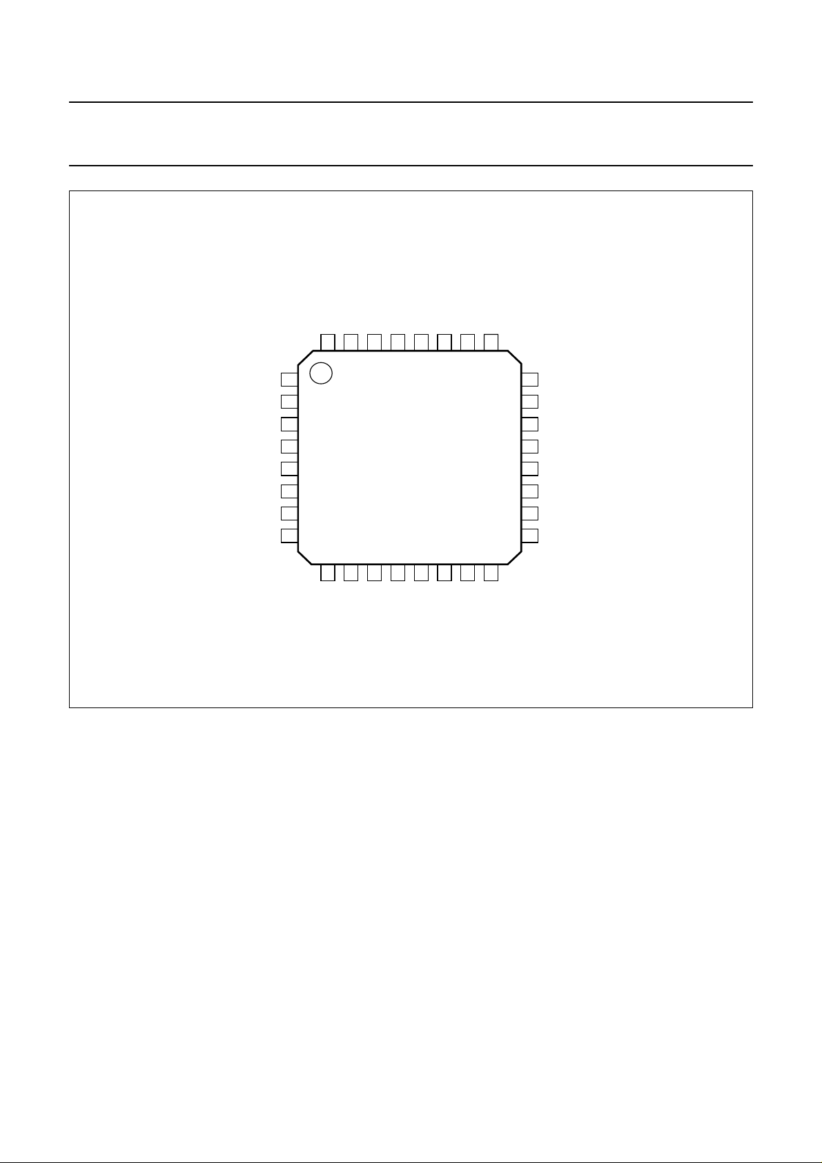
UAA3545HL LQFP32 plastic low profile quad flat package; 32 leads; body 5 × 5 × 1.4 mm SOT401-1
2001 Sep 06 2

Philips Semiconductors Product specification
Fully integrated DECT transceiver UAA3545
QUICK REFERENCE DATA
VCC= 3.2 V; T
SYMBOL PARAMETER CONDITIONS MIN. TYP. MAX. UNIT
CC(syn)
CC(reg)
CC(RX)
CC(TX)
CC(SYN)
CC(REG)
CC(RX)
CC(TX)
CC(pd)
o(RF)
(i)XTAL
PC
amb
,
,
,
V
V
V
V
I
I
I
I
I
f
f
f
T
=25°C; characteristics with a typical value only are not tested; unless otherwise specified.
amb
supply voltage All VCCsupplies
3.0 3.2 3.6 V
must be at the
same potential
)
(V
CC
synthesizer supply current synthesizer ON − 57mA
VCO, buffer and prescaler regulator
VCO ON − 14 17 mA
supply current
receiver supply current − 36 44 mA
transmit preamplifier supply current − 12 15 mA
total supply current in Power-down mode − 10 100 µA
RF output frequency 1880 − 1930 MHz
crystal reference input frequency − 3.456,
− MHz
6.912,
10.368or
13.824
phase comparator frequency − 864 − kHz
ambient temperature −10 − +60 °C
2001 Sep 06 3

Philips Semiconductors Product specification
Fully integrated DECT transceiver UAA3545
BLOCK DIAGRAM
handbook, full pagewidth
15
RFA
14
RFB
20
TXA
21
TXB
VCO_ON
R_ON
1
17
S_CLK
V
CC(RX)
16
LNA
AMP
CONTROL
LOGIC
6
8
S_DATA
S_EN
V
×
CC(TX)
22
RSSI
RXGND
12
DEMODULATORLIMITER
TXGND
13
19
SLIC = 1
UAA3545
PRESCALER
SYNTHESIZER
29
TEST3
18
23
DIVGND
VREGDIV
28 32 25
4
TEST2
TEST1
5
24 3
V
XTAL
CC(SYN)
CP/VCO
SLICER
0
V
tune
1 kΩ
(1)
VCO REGULATOR
MOD
SLIC = 1
V
CC(REG)
SLIC = 1
0
0
2
11
26
10
31
30
27
MGW108
7
9
RDATAP
DATAM
SLCCTR
VREGI
SYNGND
VREGO
REGGND
VCOGND
(1) SLCCTR ‘switches’ shown in position SLCCTR = LOW.
Fig.1 Block diagram.
2001 Sep 06 4

Philips Semiconductors Product specification
Fully integrated DECT transceiver UAA3545
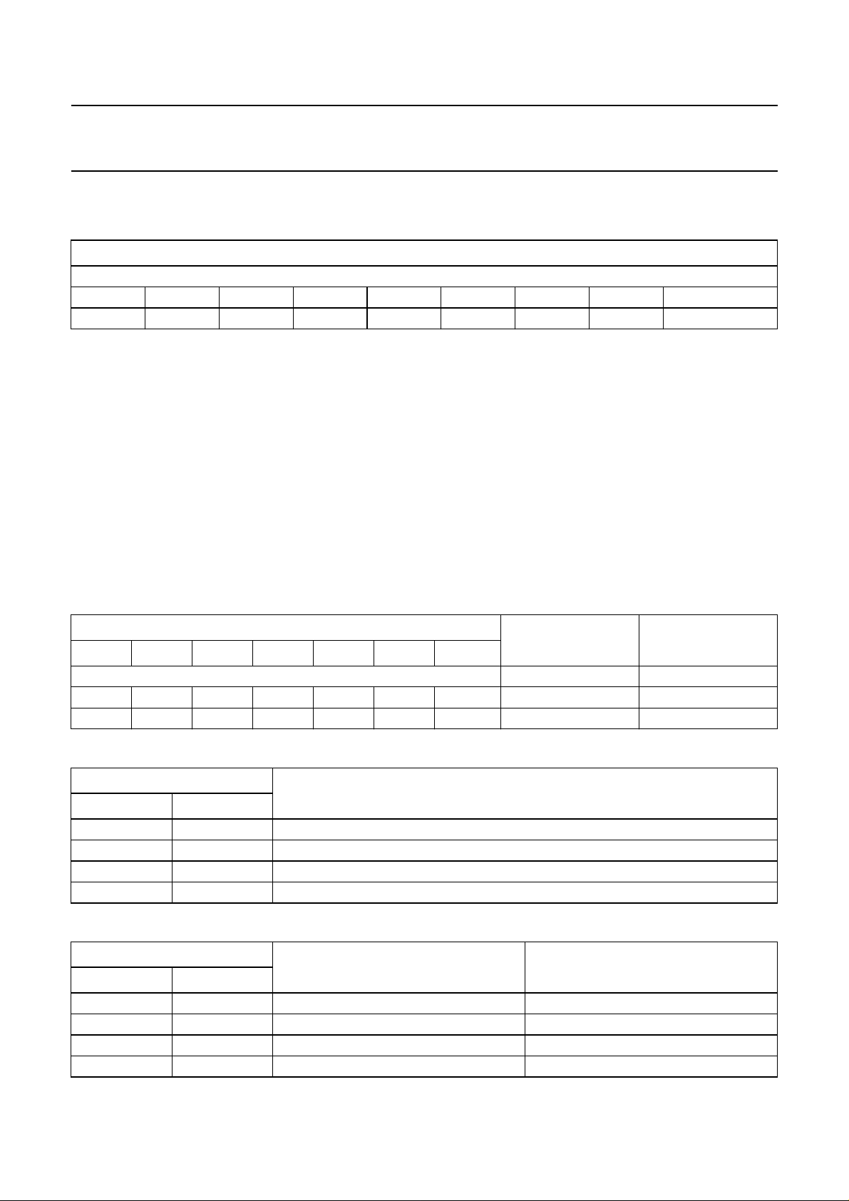
PINNING
SYMBOL PIN DESCRIPTION
VCO_ON 1 VCO section power-on control; note 1
V
CC(REG)
V
CC(SYN)
S_DATA 4 3-wire bus data signal input
XTAL 5 reference frequency input; note 2
S_EN 6 3-wire bus enable signal input
RDATAP 7 demodulator output voltage
S_CLK 8 3-wire bus clock signal input
DATAM 9 switched demodulator output voltage
SYNGND 10 synthesizer ground
SLCCTR 11 DATAM switch control signal (see Fig.1)
RSSI 12 received signal strength intensity voltage output
RXGND 13 receiver ground
RFB 14 received signal input B
RFA 15 received signal input A
V
CC(RX)
R_ON 17 receiver power-on control; note 3
TEST3 18 TEST input 3 (must be connected to GND)
TXGND 19 transmitter ground
TXA 20 transmit amplifier output A
TXB 21 transmit amplifier output B
V
CC(TX)
DIVGND 23 divider ground
VREGDIV 24 divider regulated supply voltage
V
MOD
VREGI 26 VCO regulated voltage input
VCOGND 27 VCO ground
TEST1 28 TEST input 1 (must not be connected)
TEST2 29 TEST input 2 (must not be connected)
REGGND 30 regulator ground
VREGO 31 VCO section regulated voltage output
CP/VCO
tune
2 regulator positive supply voltage
3 synthesizer positive supply voltage
16 receiver positive supply voltage
22 transmitter positive supply voltage
25 VCO analog modulation voltage input
32 charge-pump output/VCO tuning input
Notes
1. Corresponds to the S_PWR of the baseband chip (see Section “Operating modes” for more details).
2. Corresponds to the REF_CLK of the baseband chip.
3. See Section “Operating modes” for more details.
2001 Sep 06 5
Philips Semiconductors Product specification
Fully integrated DECT transceiver UAA3545
handbook, full pagewidth
VCO_ON
V
CC(REG)
V
CC(SYN)
S_DATA
RDATAP
S_CLK
XTAL
S_EN
tune
CP/VCO
VREGO
REGGND
TEST2
TEST1
VCOGND
31
32
1
2
3
4
5
6
7
8
9
DATAM
30
UAA3545HL
11
10
SLCCTR
SYNGND
29
12
RSSI
28
27
13
14
RFB
RXGND
VREGI
26
15
RFA
MOD
V
25
16
CC(RX)
V
24
23
22
21
20
19
18
17
FCA242
VREGDIV
DIVGND
V
CC(TX)
TXB
TXA
TXGND
TEST3
R_ON
Fig.2 Pin configuration.
2001 Sep 06 6

Philips Semiconductors Product specification
Fully integrated DECT transceiver UAA3545
FUNCTIONAL DESCRIPTION
Transmit chain
VCO AND PRESCALER
The fully integrated VCO operates at a multiple of the
DECT frequency. It is supplied by an on-chip voltage
regulator to minimize frequency disturbances due to
supply voltage variations. The VCO signal is fed into a
prescaler. A large difference between transmitted and
VCO frequencies reduces transmitter-oscillator coupling
problems.
The output of the prescaler drives the synthesizer main
divider. The divider output can also be switched to either
the TX preamplifier or the RX LO output buffer. The high
isolation obtained from the prescaler ensures very small
frequencychangeswhenturning-onthe TX preamplifier or
the RX section. In TX mode, the oscillator can be
modulated directly with GFSK-filtered data at pin V
MOD
.
TX PREAMPLIFIER
The TX preamplifier amplifies the RF signal to a level of
3 dBm (typical) which is suitable for use with Philips
Semiconductors DECT power amplifiers.
Synthesizer
MAIN DIVIDER
The main divider is clocked by the RF signal from the
prescaler at frequencies from 1880 to 1930 MHz. Any
main divider ratio from 2176 to 2303 inclusive can be
programmed.
REFERENCE DIVIDER
PHASE COMPARATOR
The phase comparator is driven by the output of the main
and reference dividers. It produces current pulses at
pin CP/VCO
, the pulse duration being the difference in
tune
arrival time of current pulse edges from the two dividers.
If the main divider edge arrives first, pin CP sinks current.
If the reference divider edge arrives first, pin CP sources
current. The DC value of the charge-pump current is
defined by an internal resistor. Additional circuitry is
included to ensure the gain of the phase detector remains
linear even for small phase errors.
Serial programming bus
A simple 3-line unidirectional serial bus is used to
program the circuit. The three lines are data (S_DATA),
serial clock (S_CLK) and serial bus enable (S_EN). Data
sent to the device are loaded in bursts framed by S_EN.
Programming clock edges and their appropriate data bits
are ignored until S_EN goes active (LOW). The
programmed information is read directly by the main
divider when S_EN returns to HIGH. S_DATA and S_EN
change value on the falling edge of S_CLK.
During synthesizer operation, S_EN should be held
HIGH. Only the last 24 bits clocked into the device are
retained within the serial register. Additional leading bits
are ignored and no check is made on the number of clock
pulses. The data format is shown in Table 1. The first bit
entered is b23, the last bit is b0. For the main divider ratio,
the first bit (b5) is the Most Significant Bit (MSB).
The serial bus enable (S_EN) must be LOW to capture
newprogramming data and must be HIGHto switch on the
synthesizer.
The reference divider is clocked by the signal at pin XTAL.
The circuit operates with levels from 1.2 to 1.8 V (p-p) at a
frequency of 3.456 MHz. By programming the ‘REFD’ bits
of the serial input register (see Table 1) the reference
frequency can be set for 6.912, 10.368 or 13.864 MHz.
2001 Sep 06 7

Philips Semiconductors Product specification
Fully integrated DECT transceiver UAA3545
Receiver
The receiver is a fully integrated RF + IF strip and
demodulatorfor DECT. It provides allthe required channel
filtering over the DECT band and generates analog RSSI
and a switched output for Philips Semiconductors
basebandchip.Veryfewoff-chipcomponentsarerequired
and all of these can be placed without trimming. The chip
is designed to operate with a power supply voltage that
can fall to 3.0 V. The input is the RF antenna signal
derived from the band filter or the antenna switch. The
outputs are the RSSI voltage, representing the
instantaneous signal strength and two HIGH-level
demodulator output signals RDATAP and DATAM, the
latter being switched by SLCCTR to generate the external
slicer threshold. During the blind slot, while the PLL is
settling, an internal voltage source is activated to
precharge the external capacitor (connected to
pin DATAM) to a voltage close to the required slicer
threshold.
Operating modes
The operating modes available are:
• Normal mode (see Fig.3)
• Reduced signal mode (see Fig.4)
• Advanced signal mode (see Fig.5).
Selection of an operating mode is achieved via the serial
interface register (see Table 3).
NORMAL MODE (MODE 1)
In the normal mode, the synthesizer is ON when
S_EN = HIGH and VCO_ON = HIGH, and OFF when
S_EN = LOW. When turned ON, the dividers and phase
detector are synchronized to avoid a random initial phase
error. When turned OFF, the phase detector is
synchronized with the dividers to avoid interrupting a
charge-pump pulse. This feature requires a signal to be
present for a few microseconds on the XTAL pin after
S_EN goes LOW.
The VCO is ON when the input signal VCO_ON is HIGH.
The polarity of VCO_ON is chosen for compatibility with
output S_PWR of the baseband chip. When the VCO is
turned ON, it takes 50 µs (typical) to reach its steady state.
REDUCED SIGNAL MODE (MODE 2)
Inthe reduced signal mode, the parallel control signals are
replaced by serial bus programming. To select this mode,
the bit ‘NEW’ of the internal register must be set to ‘1’ and
the bit ‘SPWR’ must be reset to ‘0’, timing is then
controlled by the S_EN signal.
After the register programming, the S_EN rising edge
programs the PLL, closes the loop, powers-on the VCO
and, if the ‘TRX’ bit = 0, turns ON the TX preamplifier.
On the falling edge of the first S_EN pulse, the loop is
opened (unless the bit ‘PLL’ is set to 1) and the receiver
switches ON if the ‘TRX’ bit = 1. A second pulse on S_EN
is required at the endof the wanted slot to power-down the
application.
The R_ON pin becomes an output in this mode, drives the
RX PIN diode and corresponds to the internal power-on
signal of the receiver.
ADVANCED SIGNAL MODE (MODE 3)
In the advanced signal mode, the parallel control signals
are partly replaced by serial bus programming. To select
this mode, the bit ‘NEW’ and the bit ‘SPWR’ of the internal
register must be set to ‘1’. The S_EN signal will then
control the UAA3545 timing (except for timing of a general
power-down as this is controlled by the VCO_ON input).
The VCO_ON signal should rise at the beginning of the
previous slot. After the serial bus has been programmed,
the S_EN rising edge programs the PLL, closes the loop
and, if the ‘TRX’ bit = 0, turns ON the TX preamplifier.
On the falling edge of the first S_EN pulse, the loop is
opened(unless the ‘PLL’ bitis set to 1) and theRX section
switches ON if bit ‘TRX’ = 1. At the end of the wanted slot,
the VCO_ON goes LOW to power-down the whole IC.
In fact, the second pulse of the S_EN signal in mode 2 is
now replaced by the signal VCO_ON.
The R_ON pin becomes an output in this mode, drives the
RX PIN diode and corresponds to the internal power-on
signal of the receiver.
The TX preamplifier is ON when bit ‘TRX’ is programmed
to ‘0’ and VCO_ON is HIGH. When the TX preamplifier is
turned ON, it takes typically 10 µs to be ready. The
receiver is turned ON when R_ON = HIGH and
VCO_ON = HIGH.
2001 Sep 06 8
Philips Semiconductors Product specification
Fully integrated DECT transceiver UAA3545
Programming
Table 1 Serial interface register
REGISTER BIT ALLOCATION
first in last in
b23 to b20 b19 b18, b17 b16 to b10 b9 b8 b7 b6 b5 to b0
TEST
(2)
SLIC
(3)
REFD
(4)
TEST
(2)
SPWR
(5)
PLL
(6)
NEW
(5)
TRX MAIN DIVIDER
Notes
1. Bit b5 is the MSB of the main divider coefficient; this comprises bits b5, b4, b3, b2, b1, b0 and b6 (TRX).
2. Test bits b23, b22, b21, b20, b16, b15, b14, b13, b12, b11, b10 must always be programmed to 0.
3. Bit ‘SLIC’ = 1 forces the internal slicer on. In this mode, pin DATAM is connected to an external capacitor. Together
with an internal 1 kΩ resistor, it defines the low pass time constant for the slicer threshold voltage. When the
bit ‘SLIC’ = 0, the pin RDATAP is connected directly to the demodulator output and delivers an analog signal.
Pin DATAM also reflects the demodulator voltage without the internal 1 kΩ resistor when the SLCCTR pin is HIGH.
4. REFD sets the reference divider ratio to 4, 8, 12 or 16 (corresponding respectively to a reference input frequency of
3.456, 6.912, 10.368 or 13.824 MHz) (see Table 4).
5. Bits ‘NEW’, and ‘SPWR’ select the operating mode (see Table 3).
6. Bit ‘PLL’ = 1 forces the PLL to remain on when the VCO is on.
7. The main divider ratio is equal to 2176 + the programmed value (see Table 2).
(1)
(7)
Table 2 Main divider programming
BIT
b5 b4 b3 b2 b1 b0 b6 (TRX)
MAIN DIVIDER
RATIO
SYNTHESIZED
FREQUENCY (MHz)
Binary equivalent of n 2176 + n 0.864 × (2176 + n)
000000 0 2176 1880.064
010111 1 2223 1920.672
Table 3 Operating mode selection
BIT
OPERATING MODE
b9 (SPWR) b7 (NEW)
0 0 normal mode (mode 1)
0 1 reduced signal mode (mode 2)
1 0 do not use
1 1 advanced signal mode (mode 3)
Table 4 Reference divider ratio programming
BIT
REFERENCE DIVIDER RATIO REFERENCE INPUT FREQUENCY
b18 b17
0 0 4 3.456 MHz
0 1 16 13.824 MHz
1 0 8 6.912 MHz
1 1 12 10.368 MHz
2001 Sep 06 9
 Loading...