


INTEGRATED CIRCUITS
DATA SH EET
TZA1038HW
High speed advanced analog DVD
signal processor and laser supply
Product specification 2003 Sep 03

Philips Semiconductors Product specification
High speed advanced analog DVD signal
processor and laser supply
CONTENTS
1 FEATURES
2 GENERAL DESCRIPTION
3 ORDERING INFORMATION
4 QUICK REFERENCE DATA
5 BLOCK DIAGRAM
6 PINNING
7 FUNCTIONAL DESCRIPTION
7.1 RF data processing
7.2 Servo signal processing
7.2.1 Servo signal path set-up
7.2.2 Focus servo
7.2.3 Radial servo
7.2.4 Differential phase detection
7.2.4.1 Drop-out concealment
7.2.4.2 Push-pull and three-beam push-pull
7.2.4.3 Enhanced push-pull (dynamic offset
compensation for beam landing)
7.2.4.4 Offset compensation
7.2.5 Automatic dual laser supply
7.2.6 Power-on reset and general power on
7.2.7 Compatibility with TZA1033HL/V1
7.2.7.1 Software compatibility
7.2.7.2 Hardware compatibility
7.2.8 Interface to the system controller
7.3 Control registers
7.3.1 Register 0: power control
7.3.2 Register 1: servo and RF modes
7.3.3 Register 2: focus offset DAC
7.3.4 Register 3: RF path gain
7.3.5 Register 4: RF left and right, or sum offset
compensation
7.3.6 Register 5: RF sum offset compensation
7.3.7 Register 6: servo gain and dynamic radial
offset compensation factor
7.3.8 Register 7: servopath gain and bandwidth and
RF path bandwidth and pre-emphasis
7.3.9 Register 8: RF channel selection
7.3.10 Register 11: radial servo offset cancellation
7.3.11 Register 12: central servo offset cancellation
inputs A and B
7.3.12 Register 13: central servo offset cancellation
inputs C and D
7.3.13 Register 14: RF filter settings
7.3.14 Register 15: DPD filter settings
TZA1038HW
7.4 Internal digital control, serial bus and external
digital input signal relationships
7.4.1 STANDBY mode
7.4.2 RF only mode
7.5 Signal descriptions
7.5.1 Data path signals through pins A to D
7.5.2 Data signal path through input pins RFSUMP
and RFSUMN
7.5.3 HF filtering
7.5.4 Focus signals
7.5.5 Radial signals
7.5.5.1 DPD signals (DVD-ROM mode) with no
drop-out concealment
7.5.5.2 DPD signals (DVD-ROM mode) with
drop-out concealment
7.5.5.3 Three-beam push-pull (CD mode)
7.5.5.4 Enhanced push-pull
8 LIMITING VALUES
9 THERMAL CHARACTERISTICS
10 CHARACTERISTICS
11 APPLICATION INFORMATION
11.1 Signal relationships
11.1.1 Data path
11.1.2 Servo path
11.2 Programming examples
11.3 Energy saving
11.4 Initial DC and gain setting strategy
11.4.1 Electrical offset from pick-up
11.4.2 Gain setting servo
11.4.3 DC level in RF path
11.4.4 Gain setting RF path
12 PACKAGE OUTLINE
13 SOLDERING
13.1 Introduction to soldering surface mount
packages
13.2 Reflow soldering
13.3 Wave soldering
13.4 Manual soldering
13.5 Suitability of surface mount IC packages for
wave and reflow soldering methods
14 DATA SHEET STATUS
15 DEFINITIONS
16 DISCLAIMERS
2003 Sep 03 2

Philips Semiconductors Product specification
High speed advanced analog DVD signal
processor and laser supply
1 FEATURES
• Operates with DVD-ROM, DVD+RW, DVD-RW,
CD-ROM and CD-RW
• Operates up to 64 × CD-ROM and 12 × DVD-ROM
• RF data amplifier with wide, fine pitch programmable
noise filter and equalizer equivalent to 64 × CD or
12 × DVD
• Programmable RF gain for DVD-ROM, CD-RW and
CD-ROM applications (approximately 50 dB range to
cover a large range of disc-reflectivity and OPUs)
• Additional RF sum input
• Balanced RF data signal transfer
• Universal photodiode IC interface using internal
conversion resistors and offset cancellation
• Input buffers and amplifiers with low-pass filtering
• Three different tracking servo strategies:
– Conventional three-beam tracking for CD
– Differential Phase Detection (DPD) for DVD-ROM,
including option to emulate traditional drop-out
detection: Drop-Out Concealment (DOC)
– Advanced push-pull with dynamic offset
compensation.
• Enhanced signal conditioning in DPD circuit for optimal
tracking performance under noisy conditions
• Radial error signal for Fast Track Counting (FTC)
• RF onlymode: servo outputs canbeset to 3-state, while
RF data path remains active
• Radial servo polarity switch
• Flexible adaption to different light pen configurations
• Two fully automatic laser controls for red and infrared
lasers, including stabilization and an on/off switch
• Automatic selection of monitor diode polarity
• Digital interface with 3 and 5 V compatibility.
TZA1038HW
2 GENERAL DESCRIPTION
The TZA1038HW is an analog preprocessor and laser
supply circuit for DVD and CD read-only players. The
device contains data amplifiers, several options for radial
tracking and focus control. The preamplifier forms a
versatile, programmable interface between single light
path voltage output CD or DVD mechanisms to Philips
digital signal processor family for CD and DVD (for
example, Gecko, HDR65 or Iguana). A separate
high-speed RFSUM input is available.
The device contains several options for radial tracking:
• Conventional three-beam tracking for CD
• Differential phase detector for DVD
• Push-pull with flexible left and right weighting to
compensate dynamic offsets e.g. beam landing offset
• A radial error signal to allow Fast Track Count (FTC)
during track jumps.
The dynamic range of this preamplifier and processor
combination can be optimized for LF servo and RF data
paths. The gain in both channels can be programmed
separately and so guarantees optimal playability for all
disc types.
The RF path is fully DC coupled. The DC content
compensation techniques provide fast settling after disc
errors.
The device can accommodate astigmatic, single foucault
anddoublefoucault detectors and can beusedwithP-type
lasers with N-sub or P-sub monitor diodes. After an initial
adjustment, the circuit will maintain control over the laser
diode current. With an on-chip reference voltage
generator, a constant stabilized output power is ensured
and is independent of ageing.
An internal Power-on reset circuit ensures a safe start-up
condition.
2003 Sep 03 3

Philips Semiconductors Product specification
High speed advanced analog DVD signal
TZA1038HW
processor and laser supply
3 ORDERING INFORMATION
TYPE NUMBER
NAME DESCRIPTION VERSION
TZA1038HW HTQFP48 plastic thermal enhanced thin quad flat package; 48 leads;
body 7 × 7 × 1 mm; exposed die pad
4 QUICK REFERENCE DATA
SYMBOL PARAMETER CONDITIONS MIN. TYP. MAX. UNIT
T
amb
ambient temperature −40 − +85 °C
Supplies
V
DDA1
V
DDA3
V
DDD3
V
DDD5
I
DD
, V
, V
DDA2
DDA4
,
analog supply voltage 4.5 5.0 5.5 V
3 V digital supply voltage 2.7 3.3 5.5 V
5 V digital supply voltage 4.5 5.0 5.5 V
supply current without laser supply − 98 120 mA
STANDBY mode −− 1mA
V
I(logic)
logic input compatibility note 1 2.7 3.3 5.5 V
Servo signal processing
B
LF(−3dB)
−3 dB bandwidth of
LF path
I
O(LF)
output current focus servo output 0 − 12 µA
radial servo output 0 − 12 µA
V
O(FTC)(p-p)
FTC output voltage
(peak-to-peak value)
B
FTC
FTC bandwidth FTCHBW = 0 − 600 − kHz
FTCHBW = 1; note 2 − 1200 − kHz
V
I(FTCREF)
FTC reference input
voltage
RF data processing
A
RF
linear current gain programmable gain
RF channels 6 − 49 dB
RFSUM channels −6 − +31 dB
B
RF(−3dB)
f
0(RF)
t
d(RF)
−3 dB bandwidth of RFP
and RFN signal path
noise filter and equalizer
corner frequency
flatness delay in RF data
path
RFEQEN = 0;
RFNFEN = 0
BWRF = 0 8 12.0 14.5 MHz
BWRF = 127 100 145 182 MHz
equalizer on; flat from
0 to 100 MHz;
BWRF = 127
Z
i
input impedance of
pins A to D
PACKAGE
SOT545-2
60 75 100 kHz
2.0 −−V
1.25 − 2.75 V
200 300 − MHz
−− 0.5 ns
100 −−kΩ
2003 Sep 03 4

Philips Semiconductors Product specification
High speed advanced analog DVD signal
TZA1038HW
processor and laser supply
SYMBOL PARAMETER CONDITIONS MIN. TYP. MAX. UNIT
V
i(RF)(FS)
V
i(SUM)(dif)
V
I(DC)
V
o(RF)(dif)(p-p)
V
O(RF)(DC)
V
i(RFREF)(CM)
Laser supply
I
o(laser)(max)
V
i(mon)
input voltage on
pins A to D for full-scale at
output
differential input voltage
on pins RFSUMP and
RFSUMN
DC input voltage range on
pins RFSUMP and
RFSUMN
differential output voltage
on pins RFP and RFN
(peak-to-peak value)
DC output voltage on
pins RFP and RFN
input reference voltage on
pin RFREF for common
mode output
maximum current output
to laser
input voltage from laser
monitor diode
atthe appropriate signal
path gain setting
RF signal path −− 600 mV
LF signal path −− 700 mV
G
with respect to V
= −6dB −− 1800 mV
RFSUM
SS
1.3 − V
DDA
− 1.0 V
−− 1.4 V
0.35 − V
DDA
− 1.9 V
0.8 1.2 2.1 V
−120 −−mA
P-type monitor diode
LOW level voltage − V
HIGH level voltage − V
− 0.155 − V
DDA4
− 0.190 − V
DDA4
N-type monitor diode
LOW level voltage − 0.155 − V
HIGH level voltage − 0.185 − V
Notes
1. Input logic voltage level follows the supply voltage applied at pin V
2. High FTC bandwidth is achieved when IS1and IS2> 1.5 µA.
2003 Sep 03 5
DDD3
.
Philips Semiconductors Product specification
High speed advanced analog DVD signal
processor and laser supply
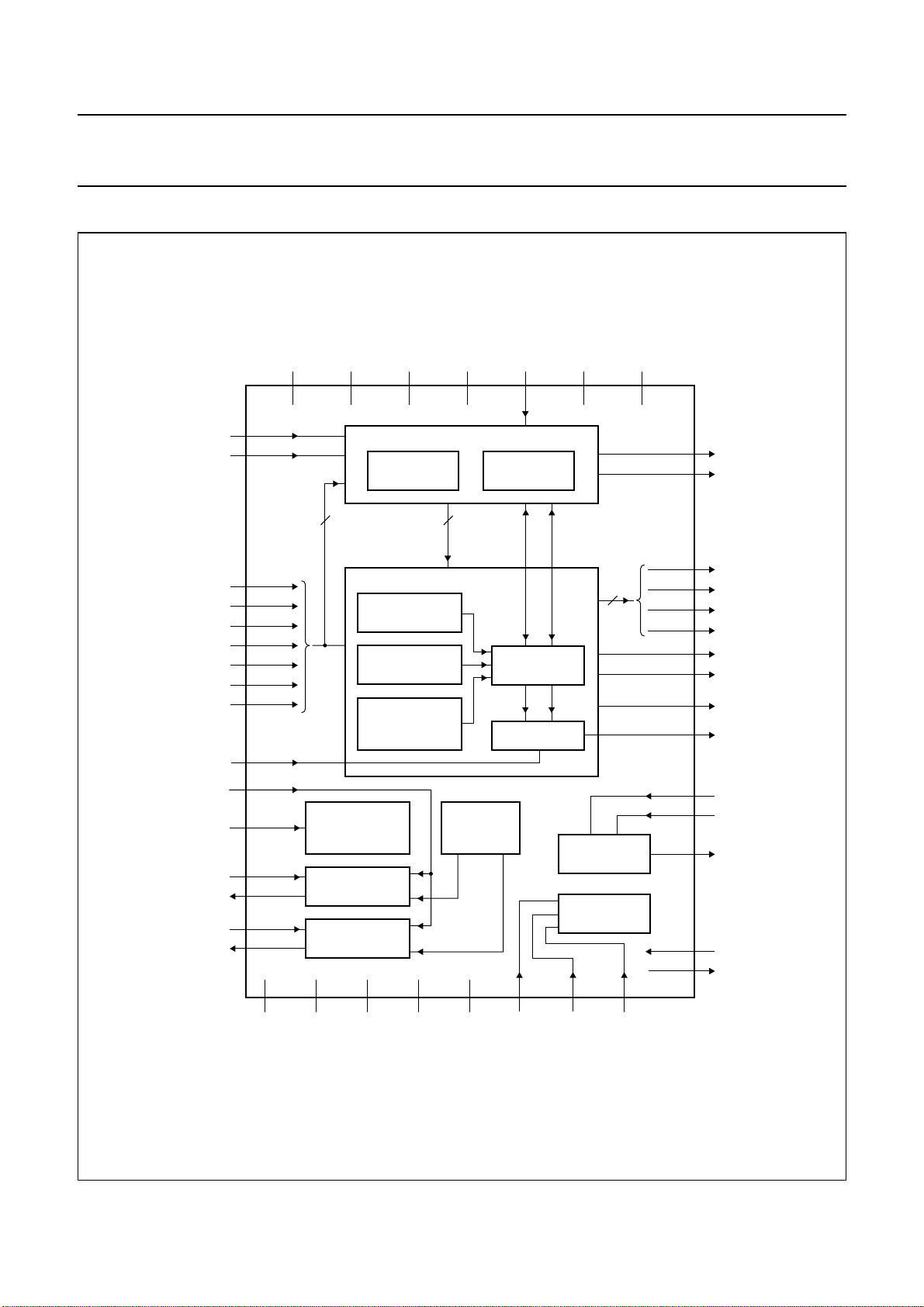
5 BLOCK DIAGRAM
handbook, full pagewidth
RFSUMP
RFSUMN
OPUREF
FTCREF
V
DDL
REXT
CDMI
CDLO
DVDMI
DVDLO
V
DDA1
1
2
OPUREF
8
A
9
B
10
C
11
D
3
E
4
F
12
27
47
44
46
45
7
48
6
V
SSA1
5
A to D
5
VOLTAGE AND
REFERENCES
42
V
SSA2
V
DDA2
CURRENT
LASER 1
LASER 2
V
DDA3
43
SERVO SIGNAL PROCESSING
COMPENSATION
V
SSA3
37
RF DATA PROCESSING
MULTIPLEXER
4
3-BEAM
TRACKING
DPD
PUSH-PULL
OFFSET
41
V
SSA4
31
V
DDA4
DUAL
LASER
SUPPLY
V
SSD
RFREF
32
VARIABLE
GAIN STAGES
SELECT; SWAP
S1 S2
19
SIDA
38
FTC
16
V
DDD3
V
15
TZA1038HW
4
FTC
COMPARATOR
SERIAL
INTERFACE
17 18
SICL SILD
DDD5
23
TZA1038HW
39
RFP
40
RFN
36
OA
35
OB
34
OC
33
OD
30
S1
29
S2
28
OCENTRAL
25
FTC
20
COP
21
COM
22
COO
14
TM
26
TDO
MCE466
Fig.1 Block diagram.
2003 Sep 03 6

Philips Semiconductors Product specification
High speed advanced analog DVD signal
processor and laser supply
6 PINNING
SYMBOL PIN DESCRIPTION
RFSUMP 1 positive RF sum input
RFSUMN 2 negative RF sum input
E 3 input E
F 4 input F
V
DDA1
V
SSA1
DVDMI 7 input signal from DVD laser monitor diode
A 8 input A
B 9 input B
C 10 input C
D 11 input D
OPUREF 12 reference input from Optical Pick-Up (OPU)
n.c. 13 not connected
TM 14 test mode input (factory test only)
V
DDD3
SIDA 16 serial host interface data input
SICL 17 serial host interface clock input
SILD 18 serial host interface load
V
SSD
COP 20 positive FTC comparator input
COM 21 inverting FTC comparator input
COO 22 FTC comparator output
V
DDD5
n.c. 24 not connected
FTC 25 fast track count output
TDO 26 test data output (factory test only)
FTCREF 27 FTC reference input
OCENTRAL 28 test pin for offset cancellation
S2 29 servo current output 2 for radial tracking
S1 30 servo current output 1 for radial tracking
V
SSA4
V
DDA4
OD 33 servo current output for focus D
OC 34 servo current output for focus C
OB 35 servo current output for focus B
OA 36 servo current output for focus A
V
DDA3
RFREF 38 DC reference input for RF channel common mode output voltage
RFP 39 positive RF output
RFN 40 negative RF output
5 analog supply voltage 1 (RF input stage)
6 analog ground 1
15 digital supply voltage (serial interface 3 V I/O pads and FTC comparator)
19 digital ground
23 digital supply voltage (5 V digital core)
31 analog ground 4
32 analog supply voltage 4 (servo signal processing)
37 analog supply voltage 3 (RF output stage)
TZA1038HW
2003 Sep 03 7

Philips Semiconductors Product specification
High speed advanced analog DVD signal
processor and laser supply
SYMBOL PIN DESCRIPTION
V
SSA3
V
SSA2
V
DDA2
REXT 44 reference current input (connect via 12.1 kΩ to V
CDLO 45 CD laser output
CDMI 46 input signal from CD laser monitor diode
V
DDL
DVDLO 48 DVD laser output
41 analog ground 3
42 analog ground 2
43 analog supply voltage 2 (internal RF data processing)
47 laser supply voltage
SSA4
TZA1038HW
)
handbook, full pagewidth
RFSUMP
RFSUMN
V
DDA1
V
SSA1
DVDMI
OPUREF
SSA3
SSA2
DDL
CDLO
CDMI
V
DVDLOn.c.
48
47
46
45
1
2
3
E
4
F
5
6
7
8
A
9
B
10
C
D
11
12
13
14
15
16
TM
SIDA
DDD3
V
DDA2
V
V
REXT
43
42
44
TZA1038HW
17
18
19
SILD
SSD
V
SICL
V
41
20
COP
RFN
40
21
COM
RFP
39
22
COO
RFREF
38
23
DDD5
V
DDA3
V
37
24
n.c.
36
OA
35
OB
34
OC
33
OD
V
32
V
31
30
S1
29
S2
28
OCENTRAL
27
FTCREF
26
TDO
25
FTC
MCE467
DDA4
SSA4
Fig.2 Pin configuration.
2003 Sep 03 8

Philips Semiconductors Product specification
High speed advanced analog DVD signal
processor and laser supply
7 FUNCTIONAL DESCRIPTION
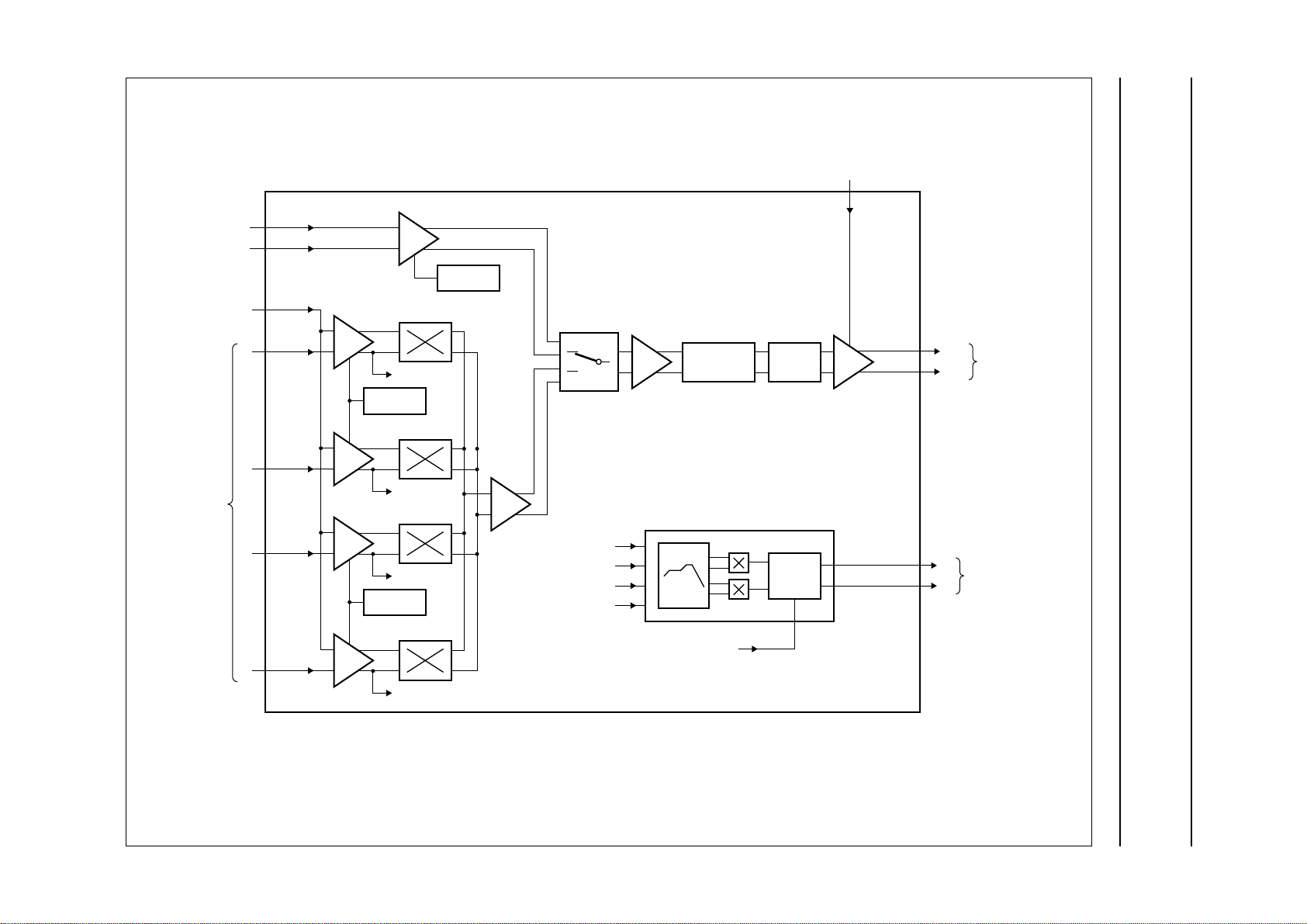
7.1 RF data processing
The RF data path is a fully DC-coupled, multi-stage
amplifier (see Fig.3). The input signal for data can be
selected from RF inputs A to D or from the summed
RF inputsRFSUMPandRFSUMN.Switchingbetweenthe
two sets of signals is performed by an internal multiplexer.
The signals are fully balanced internally to improve signal
quality and reduce power supply interference.
RF outputs RFP and RFN can be DC coupled to the
Analog-to-Digital Converter (ADC) of the decoder.
The RF input signals are from photodiodes and have
a largeDC content by nature. This DCcomponentmust be
removed from the signals for good system performance.
Built-in DACs, located after the input stages
G1and RFSUM,have the ability to dothis. The DAC range
and resolution is scaled with the gain setting of the first
amplifier stage. When the DC content is removed, the
RF signal can be DC coupled to the decoder. The main
advantage of DC coupling is fast recovery from signal
swings due to disc defects since there is no AC coupling
capacitance to slow the recovery. When using DC
coupling, both AC and DC content in the data signal is
known. The Philips Iguana decoders have on-chip control
loops to support Automatic Gain Control (AGC) and DC
cancellation.
Two separate DACs are available for cases where the left
and right side DC conditions can be different.
TZA1038HW
When it is not possible to have a DC connection between
the TZA1038HW and the decoder, the signals on servo
outputs OA to OD can be used as they contain the same
LP-filtered and DC coupled information.
Summing of the photodiode signals A to D is performed in
the second amplifier stage G2. Each individual diode
channel can be switched on, off or inverted with switches
SW-A to SW-D.
Switching between photodiode signals and RFSUM input
is performed immediately before the third amplifier
stage G3. This stage has a variable gain with fine
resolution to allow automatic gain adjustment to be
controlled by the decoder.
The filter stage limits the bandwidth according to the
maximum playback speed of the disc. This is to optimize
the noise performance. The filter stage consists of an
equalizer and a noise filter, both of which can be
bypassed,alsothe boost factor of the equalizer canbeset.
Thecorner frequencies ofthe equalizer and noisefilter are
equal and can be programmed to a 7-bit resolution.
The RF output signals RFP and RFN can be DC coupled
to a decoder with a differential input pair (as with Philips
Iguana decoders). The common mode output voltage can
be set externally at pin RFREF.
The signals for differential phase detection are tapped
from the inputs A to D at the RF amplifier G1stages.
DC cancellation for the A to D and RFSUM signal paths
can be set independently or simultaneously.
2003 Sep 03 9
This text is here in white to force landscape pages to be rotated correctly when browsing through the pdf in the Acrobat reader.This text is here in
a
_white to force landscape pages to be rotated correctly when browsing through the pdf in the Acrobat reader.This text is here inThis text is here in
white to force landscape pages to be rotated correctly when browsing through the pdf in the Acrobat reader. white to force landscape pages to be ...
2003 Sep 03 10
ndbook, full pagewidth
RFREF
Philips Semiconductors Product specification
High speed advanced analog DVD signal
processor and laser supply
RFSUMP
RFSUMN
OPUREF
RF
inputs
38
39
RFP
RFN
outputs
servo
radial
outputs
RF
40
30
S1
29
S2
TZA1038HW
MCE468
RF
RF
DPD-A
OFFSL
DPD-B
DPD-C
OFFSR
DPD-D
RFSUM
SW-A
SW-B
SW-C
SW-D
RF
OFFSS
G
3
EQUALIZER
NOISE
FILTER
TZA1038HW
G
2
DPD-A
DPD-D
DPD-C
DPD-B
central aperture signal
DPD
FILTER
DOC
1
2
12
G
8
A
9
B
10
C
11
D
1
G
1
G
1
G
1
Fig.3 RF data and DPD processing.
Philips Semiconductors Product specification
High speed advanced analog DVD signal
processor and laser supply
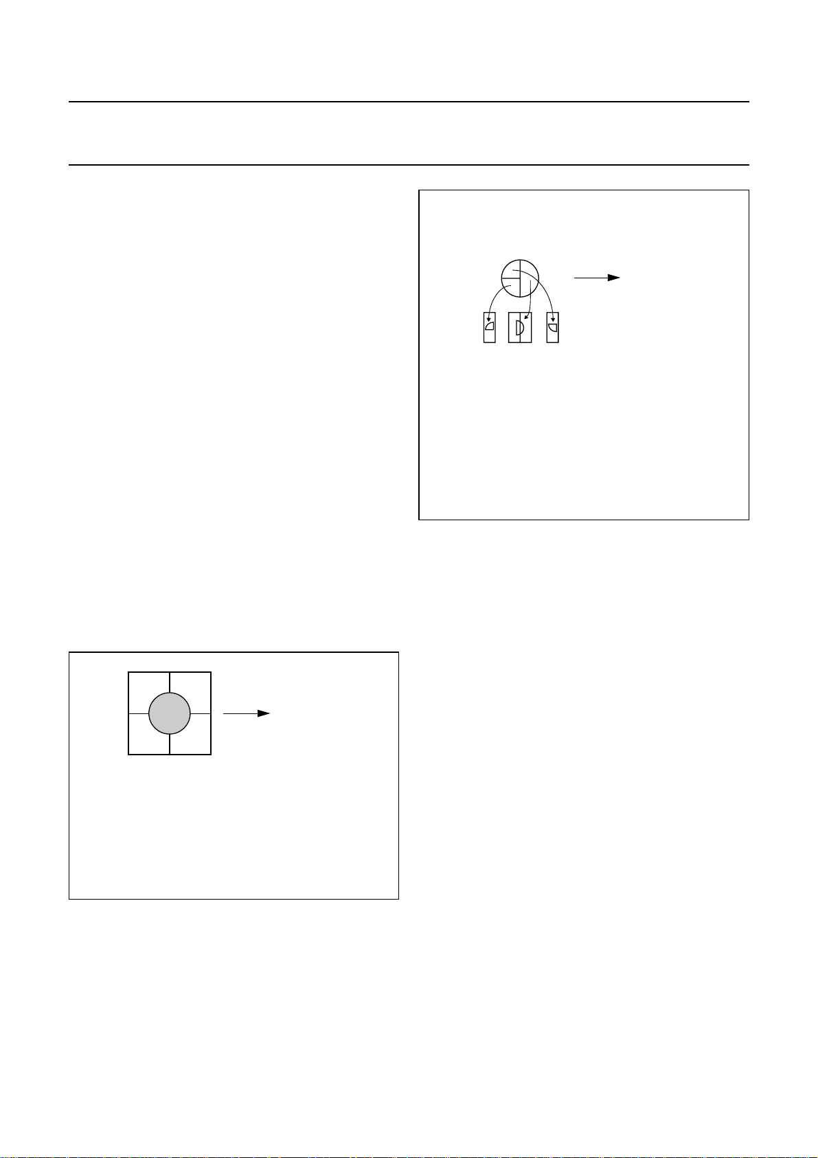
7.2 Servo signal processing
The photodiode configurations and naming conventions
are shown in Figs 4 and 5.
7.2.1 SERVO SIGNAL PATH SET-UP
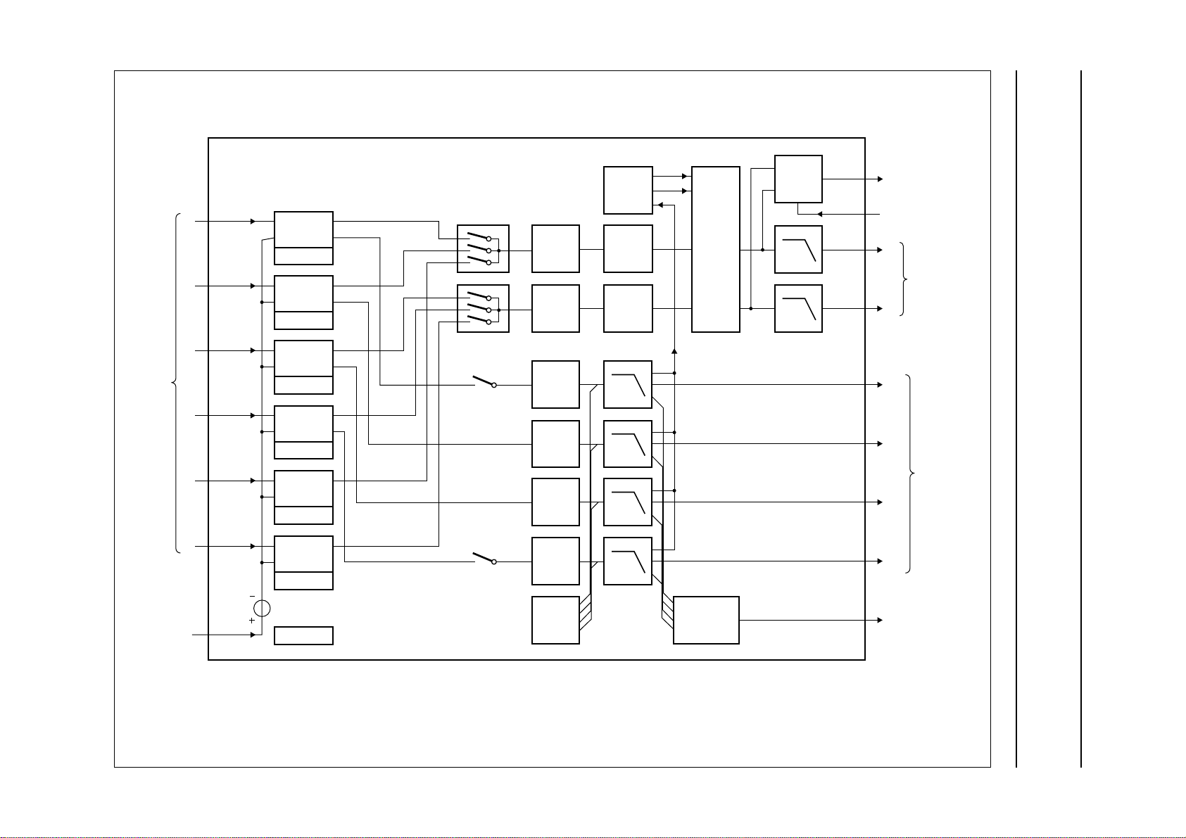
A block diagram of theservo signal path is shown in Fig.6.
In general, the servo signal path comprises:
• Avoltage-to-currentconverterwith programmable offset
voltage source V
• A 4-bit DAC for each of the six channels to compensate
for offset per channel
• A variable gain stage to adapt the signal level to the
specific pick-up and disc properties
• Low-pass filtering and output stage for the photodiode
current signals
• Error output stage in the radial data path for fast track
counting.
Servo output signals OA to OD, S1 and S2 are unipolar
current signals which represent the low-pass filtered
photodiode signals. In DPD radial tracking, the S1 and S2
signalsaretheequivalentofthe satellite signals commonly
found in traditional CD systems.
The servo output signals OA to OD, S1 and S2 are set to
3-state if bit RFonly = 1 (register 13, bit 11).
handbook, halfpage
Data=A+B+C+D
Push-pull = (A + B) − (C + D)
Focus = (A + C) − (B + D)
DPD2 = phase (A + B, C + D)
DPD4 = phase (A,D) + phase (C,B)
that is common to all inputs
LFOFFS
BA
CD
left
tangential direction
right
MGW553
TZA1038HW
handbook, halfpage
Data=A+B+C+D
Push-pull = A − D
Focus = C − B
DPD2 = phase (A, D)
DPD4 not applicable
Fig.5 Foucault diode configuration.
7.2.2 F
OCUS SERVO
Focus information is reflected in the four outputs
OA to OD. Gain and offset can be programmed.
For optical pick-ups where only channels B and C are
used for focus, channels A and D can be switched off
(bit Focus_mode = 0).
For initial alignment, a copy of the output currents can be
made available on pin OCENTRAL.
7.2.3 RADIAL SERVO
Radial information can be obtained from the two output
signals S1 and S2, and the gain and offset can be
programmed. The TZA1038HW provides differential
phase detection, push-pull and three-beam push-pull for
radial tracking. The signal FTC is made available for fast
track counting and is primarily the voltage error signal
derived from signals S1 or S2.
left
tangential direction
right
DCBA
MGW554
Fig.4 Astigmatic diode configuration.
2003 Sep 03 11
Thepolarityofthe radial loop can be reversed via theserial
control bus (RAD_pol).
This text is here in white to force landscape pages to be rotated correctly when browsing through the pdf in the Acrobat reader.This text is here in
a
_white to force landscape pages to be rotated correctly when browsing through the pdf in the Acrobat reader.This text is here inThis text is here in
white to force landscape pages to be rotated correctly when browsing through the pdf in the Acrobat reader. white to force landscape pages to be ...
2003 Sep 03 12
ndbook, full pagewidth
Philips Semiconductors Product specification
High speed advanced analog DVD signal
processor and laser supply
RF
inputs
DPD
8
A
9
B
10
C
11
D
3
E
4
F
V
/
C
OFFSA
V
/
C
OFFSB
V
/
C
OFFSC
V
/
C
OFFSD
V
/
R
OFFSE
V
/
R
OFFSF
26k
I
14k
30k
I
14k
30k
I
14k
30k
I
14k
15k
I
15k
I
MUX
2−α
G
G
G
G
α
LFC
LFC
LFC
LFC
G
G
LFR
LFR
MUX
SWAP
CA
FTC
25
FTC
27
FTCREF
30
S1
servo
radial
S2
OA
OB
OC
OD
outputs
servo
focus
outputs
29
36
35
34
33
OPUREF
V
LFOFFS
12
LF
OFFS
TZA1038HW
F
OFFS
OCENTRAL
28
MCE469
OCENTRAL
TZA1038HW
Fig.6 Servo signal path.

Philips Semiconductors Product specification
High speed advanced analog DVD signal
processor and laser supply
7.2.4 DIFFERENTIAL PHASE DETECTION
The TZA1038HW provides differential phase detection to
support DVD in various ways:
• DPD2withfour channels programmed to be activegives
DPD as required in the standard specification
• Two of the four channels can be excluded from the DPD
for pick-ups with analternative photodiode arrangement
• An increase in performance, dedicated for DVD+RW,
can be obtained by using the DPD4 method. Then two
truly separated phase detectors are active. After the
phase detection of the two input pairs the result is
summed.
InputsignalsforDPD are taken from input pins A to D after
thefirst gain stage G1(seeFig.3). Pre-emphasis is applied
by means of a programmable lead/lag filter. Additionally, a
programmable low-pass filter is available to improve the
signal quality under noisy signal conditions at lower
speeds. For further signal improvements the DPD pulse
stretcher can be programmed to higher values at lower
speeds.
The DPD signal is low-pass filtered by two internal
capacitors. The signal is then fed to pins S1 and S2, or
directedviathe drop-out concealment circuit to theoutputs
(see Section 7.5).
7.2.4.1 Drop-out concealment
A special function is built in for compatibility with drop-out
detection strategies, based on level detection in the
S1 and S2 signals. When using DPD in a fundamental
way, there is no representation of mirror level information
from the light pen.
When the drop-out concealment function is enabled
(bit DOCEN = 1), a portion of the Central Aperture (CA)
signal is added to S1 and S2. Also, when the CA signal
drops below the DOC threshold, the DPD signal is
gradually attenuated.
The DPD detection cannot work properly when the input
signal becomes very small. The output of the DPD may
then show a significant offset. The DOC may not conceal
this offset completely because:
• DOC is gradually controlled from the CA signal
• The CA signal may not become 0 during disc-defect.
For details see Section 7.5.5.2
7.2.4.2 Push-pull and three-beam push-pull
The TZA1038HW can also provide radial information by
means of push-pull signals (from the photodiodeinputs) or
TZA1038HW
in a three-spot optical system with Three-Beam Push-Pull
(TBPP). The built-in multiplexer gives a flexible method of
dealing with many detector arrangements. For push-pull,
the input signals are taken from channels A to D. There is
also a command that switches off channels B and C,
leaving channels A and D for push-pull
(bits RT_mode[2:0]).
ForTBPP, the input signal is takenfromchannels E and F,
irrespective of bit RFSUM setting.
7.2.4.3 Enhanced push-pull (dynamic offset
compensation for beam landing)
Thisoptioncancels offsets due to beam landing.Afactor α
canbe programmed to re-balancethe signal gain between
channels S1 and S2. In a simplified form this can be
described as:
S1 = A
S2 = A
Factor α can be programmed in a range from 0.6 to 1.35,
with 1.0 as the balanced condition (bits α[3:0]).
7.2.4.4 Offset compensation
A provision is made to compensate electrical offset from a
light pen. The offset voltage from the light pen can be
positiveornegative.In general, the offset between any two
channels is smaller than the absolute offsets. As negative
input signals cannot be handled by the TZA1038HW
internal servo channels, a two-step approach is adopted:
• A coarse DAC, common to all the input channels, adds
an offset that shifts the input signals in positive direction
until all inputs are ≥0. The DAC used (LF
2-bit resolution (bits LF
• A fine setting per channel is provided to cancel the
remainder of the offset between the channels. This is
achieved by DACs subtracting the DC component from
thesignalsandbringingtheinputs to approximately zero
offset (within ≈ 1 mV). The DACs (registers 11 to 13)
have a 4-bit resolution.
The range of both DACs can be increased by a factor of
three to compensate for higher offset values by means of
control parameter bit SERVOOS.
With a switched-off laser, the result of the offset
cancellation can be observed at each corresponding
output pin, OA to OD, S1 and S2, or via a built-in
multiplexer to pin OCENTRAL (central channels only).
See registers 11 to 13 for DAC and multiplexer control.
×α×input left
LFR
× (2 −α)×input right.
LFR
OFF
[1:0]).
OFFS
) has a
2003 Sep 03 13

Philips Semiconductors Product specification
High speed advanced analog DVD signal
processor and laser supply
7.2.5 AUTOMATIC DUAL LASER SUPPLY
The TZA1038HW can control the output power of two
lasers; it has an Automatic Laser Power Control (ALPC)
that stabilizes the laser output power and compensates
the effects of temperature and ageing of the laser.
ALPC automatically detects if there is a P-type or N-type
monitor diode in use in either of the laser circuits. The
regulation loop formed by the ALPC, the laser, the monitor
diode and the associated adjustment resistor will settle at
themonitorinputvoltage. The monitor input voltage can be
programmed to HIGH (≈ 180 mV) or LOW (≈ 150 mV),
according to frequently-used pre-adjustments of the light
pen. This set point can be set independently for both
ALPCs. Bandwidth limitation and smooth switch-on
behaviour is realized using an internal capacitor.
A protection circuit is included to prevent laser damage
dueto dips in laser supplyvoltage V
dip occurs, the output can saturate and restrict the
required laser current. Without the protection circuit, the
ALPC would try to maximize the output power with
destructive results for the laser when the supply voltage
recovers. The protection circuit monitors the supply
voltage and shuts off the laser when the voltage drops
belowasafe value. The ALPC recovers automaticallyafter
the dip has passed.
Only one laser can be activated at the same time.
An internal break-before-make circuit ensures safe
start-up for the laser when a toggle situation between the
two lasers is detected. When both lasers are programmed
on, neither laser will be activated.
7.2.6 POWER-ON RESET AND GENERAL POWER ON
When the supply voltage is switched on, bit PWRON is
reset by the Power-On Reset (POR) signal. This
concludes in a STANDBY mode at power up. POR is
intended to prevent the lasers being damaged due to
randomsettings.Allotherfunctionsmay be switched when
power is on. The TZA1038HW becomes active when
bit PWRON = 1.
.If a supply voltage
DDL
TZA1038HW
7.2.7 COMPATIBILITY WITH TZA1033HL/V1
7.2.7.1 Software compatibility
The TZA1038HW is highly software compatible with the
TZA1033HL/V1. Provided that some conditions are met,
the software of the TZA1038HW can be used as a
successor with just minor modifications. This compatibility
is achieved with the implementation of the TZA1038HW
mode control bit (bit K2_Mode). When bit K2_Mode = 0,
the TZA1038HW will act as a TZA1033HL/V1. When
bit K2_Mode = 1, the TZA1038HW will act as a
TZA1033HL/K2 and the new functions will be available
(but require a software update).
Other conditions or restrictions are:
• Registerbits of the TZA1038HW whichwere not defined
areprogrammedto a logic 0. Registers 9, 10, 14 and 15
may be left undefined
• The G4stage high gain setting of the TZA1033HL/V1 is
not available in the TZA1038HW; if this value was set to
logic 0, there will be no difference
• Whenbit K2_Mode = 0the RF bandwidth will be fixed to
theminimumvalueof10 MHz(typical);bit K2_Mode = 1
toselect a higher bandwidth; the bandwidthisnow lower
than using a TZA1033HL/V1.
7.2.7.2 Hardware compatibility
Thepackageis changed from LQFP64 for theTZA1033HL
to LQFP48 for the TZA1038HW.
The hardware differences are:
• Input pins STB, HEADER and LAND of the TZA1033HL
are not present
• Input pins CD of TZA1033HL/V1 are not used;
TZA1038HW has RFSUM inputs instead; the RFSUM
inputs of TZA1038HW may be connected to ground
when not used.
2003 Sep 03 14

Philips Semiconductors Product specification
High speed advanced analog DVD signal
processor and laser supply
7.2.8 INTERFACE TO THE SYSTEM CONTROLLER
Programming the registers of TZA1038HW is done via a
serial bus (see Fig.7). The circuitry is formed by a serial
input shift register and a number of registers that store the
data. The registers can always be programmed,
irrespective of STANDBY mode.
If required, the bus lines can be connected in parallel with
an I2C-bus. The protocol needs no switching of the data
line during SICL = HIGH. This means that other I2C-bus
devices will not recognise any START or STOP
commands. Control words addressed to TZA1038HW
handbook, full pagewidth
SICL
SIDA
TZA1038HW
should go uniquely with the SILD signal. When
SILD = HIGH, the TZA1038HW will not respond to any
signal on SIDA or SICL.
During a transmission, the serial data is first stored in an
input shift register. At the rising edge of SILD, the content
of the input register is copied into the addressed register.
This is also the moment the programmed information
becomes effective.
The input pins have CMOS compatible thresholdlevels for
both 3.3 and 5 V supplies.
A3D0 D1 D2 D3 D4 D5 D7 D8 D9 D10D6 D11 A0 A1 A2 D0 D1 D2 D3 A2A1D4 A3
t
load(H)
SILD
MGW496
Fig.7 Two word transmission.
7.3 Control registers
The TZA1038HW is controlled by serial registers. To keep programming fast and efficient, the control bits are sent in
16-bit words. Four bits of the word are used for the address and for each address there are 12 data bits.
Table 1 Overview of control parameters
SYMBOL PARAMETER VALUES REGISTER BITS
Data path
G
) gain of first RF amplifier stage
1(A1
0, 6 and 12 dB (1×, 2× and 4×) 3 11 and 10
(or linear amplification)
) gain of second RF amplifier
G
2(A2
6, 12, 18 and 24 dB (2×, 4×, 8× and 16×) 3 9 and 8
stage (or linear amplification)
G
) gain of third RF amplifier
3(A3
0 to 13 dB in steps of 0.8 dB (1× to 4×)37to4
stage (or linear amplification)
GRFSUM
(A
RFSUM
)
gain of RFSUM input stage (or
linear amplification)
BWRF bandwidth limitation in
−6, 0, 6, 12 and 18 dB
0 7 to 5
(0.5×,1×,2×,4×and 8×)
= 12 to 145 MHz 14 6 to 0
f
0(RF)
RF path
2003 Sep 03 15

Philips Semiconductors Product specification
High speed advanced analog DVD signal
TZA1038HW
processor and laser supply
SYMBOL PARAMETER VALUES REGISTER BITS
RF
OFFSL
RF
OFFSR
RF
OFFSS
Servo radial path
LF
OFFS
R
LFR
R
LFPP
R
OFFSE
R
OFFSF
α dynamic radial offset
I
(FS)(DPD),
I
(FS)(DPD)(DOC)
I
REFRAD(CM)
f
start_DPD
DC offset compensation in left
RF input path
DC offset compensation in
right RF input path
DC offset compensation in
RFSUM path
DC offset compensation for
LF path (common for all servo
inputs)
CD satellite path input
transresistance
DVD push-pull signal
transresistance
DC offset compensation for
radial servo path (input E)
DC offset compensation for
radial servo path (input F)
compensation factor
full scale DPD current, fixed
value based on bandgap
voltage across external
resistor
internally generated common
mode DC reference current in
DPD mode
start frequency lead/lag filter
of DPD block
RFSUM = 0; full range depends on
411to6
G1setting:
G
= 0 dB: 0 to 450 mV in 7.1 mV steps
1
G
= 6 dB: 0 to 225 mV in 3.6 mV steps
1
G
= 12 dB: 0 to 120 mV in 1.9 mV steps
1
RFSUM = 0; full range depends on
4 5 to 0
G1setting:
= 0 dB: 0 to 450 mV in 7.1 mV steps
G
1
G
= 6 dB: 0 to 225 mV in 3.6 mV steps
1
G
= 12 dB: 0 to 120 mV in 1.9 mV steps
1
RFSUM = 1; full range depends on
4or5 5to0
GRFSUM setting:
GRFSUM = −6 dB; 0 to 1700 mV
GRFSUM = 0 dB; 0 to 850 mV
GRFSUM = 6 dB; 0 to 425 mV
GRFSUM = 12 dB; 0 to 210 mV
GRFSUM = 18 dB; 0 to 105 mV
SERVOOS = 0:
V
=0,5,10or15mV
LFOFFS
11 11 and 10
SERVOOS = 1:
V
= 0, 15, 30 or 45 mV
LFOFFS
15 kΩ fixed −−
30 kΩ fixed −−
SERVOOS = 0: V
SERVOOS = 1: V
SERVOOS = 0: V
SERVOOS = 1: V
ROFFSE
ROFFSE
ROFFSF
ROFFSF
= 0 to 20 mV 11 7 to 4
= 0 to 60 mV
=0to20mV 11 3to0
=0to60mV
α = 0.6 to 1.35 in 15 steps of 0.05 6 3 to 0
DOCEN = 0: fixed value = 20 µA15
DOCEN = 1: fixed value = 6.6 µA
3.5 µA fixed −−
f
start_DPD
= 1, 5 or 10 MHz
7 1 and 0
(TZA1033HL/V1 compatible)
f
start_DPD
= 1, 5, 10, 18 or 24 MHz 15 5 to 3
2003 Sep 03 16

Philips Semiconductors Product specification
High speed advanced analog DVD signal
TZA1038HW
processor and laser supply
SYMBOL PARAMETER VALUES REGISTER BITS
G
LFR(ALFR
R
FTC
Servo focus path
R
LFC
C
OFFSA
C
OFFSB
C
OFFSC
C
OFFSD
G
LFC(ALFC
β focus offset compensation β =0to
F
OFFSEN
) lowfrequency gain, radialpath
output stage (or linear
amplification)
gain of fast track count output 680 kΩ±20% fixed for ±2 V (p-p) −−
LF path input transresistance 14 kΩ fixed −−
DC offset compensation for
central servo path A
DC offset compensation for
central servo path B
DC offset compensation for
central servo path C
DC offset compensation for
central servo path D
) low frequency gain, central
path output stage (or linear
amplification)
full range offset compensation
for focus
−15 to +9 dB in steps of 3 dB
611to8
(0.18× to 2.8×)
SERVOOS = 0: 0 to 20 mV 12 7 to 4
SERVOOS = 1: 0 to 60 mV
SERVOOS = 0: 0 to 20 mV 12 3 to 0
SERVOOS = 1: 0 to 60 mV
SERVOOS = 0: 0 to 20 mV 13 7 to 4
SERVOOS = 1: 0 to 60 mV
SERVOOS = 0: 0 to 20 mV 13 3 to 0
SERVOOS = 1: 0 to 60 mV
−15 to +9 dB in steps of 3 dB
6 7 to 4
(0.18× to 2.8×)
31
⁄
32
DAC enabled: I
DAC disabled: I
= 400 nA (fixed) 2 10
FOFFS
=0nA
FOFFS
2 4 to 0
7.3.1 REGISTER 0: POWER CONTROL
Table 2 Register address 0H
BIT 15 14 13 12 11 10 9 8
SYMBOL
AD3 AD2 AD1 AD0 −−−−
BIT76543210
SYMBOL
GRF
SUM2
GRF
SUM1
GRF
SUM0
DVD_ MILVL CD_MILVL DVD_ LDON CD_LDON PWRON
Table 3 Description of register bits (address 0H)
BIT SYMBOL FUNCTION
15 to 12 AD[3:0] 0000 = address 0H
11 to 8 − not used
7 to 5 GRFSUM[2:0] Gain of RFSUM input stage.
000 = −6dB
001 = 0 dB
010 = 6 dB
011=12dB
100=18dB
4 DVD_MILVL DVD monitor input level. 0 = 150 mV; 1 = 180 mV.
2003 Sep 03 17

Philips Semiconductors Product specification
High speed advanced analog DVD signal
TZA1038HW
processor and laser supply
BIT SYMBOL FUNCTION
3 CD_MILVL CD monitor input level. 0 = 150 mV; 1 = 180 mV.
2 DVD_LDON DVD laser on. 0 = laser off; 1 = laser on.
1 CD_LDON CD laser on. 0 = laser off; 1 = laser on.
0 PWRON Power on. 0 = STANDBY mode; 1 = power on.
7.3.2 REGISTER 1: SERVO AND RF MODES
Table 4 Register address 1H
BIT 15 14 13 12 11 10 9 8
SYMBOL
BIT76543210
SYMBOL
Table 5 Description of register bits (address 1H)
AD3 AD2 AD1 AD0 DPD_DCC −−RAD_pol
−−DOCEN Focus_
mode
RT_mode2 RT_mode1 RT_mode0 RFSUM
BIT SYMBOL FUNCTION
15 to 12 AD[3:0] 0001 = address 1H
11 DPD_DCC RF offset DAC for DPD signal control. 0 = DAC controlled by register 4,
bits RF
10 and 9 − not used
8 RAD_pol Radial polarity switch. 0 = inverse; 1 = normal (default).
7 and 6 − not used
5 DOCEN Drop-out concealment enable. 0 = disable; 1 = enable.
4 Focus_mode Focus mode. 0 = two-channel focus (channels B and C only); 1 = four-channel
focus.
3 to 1 RT_mode[2:0] Radial tracking mode.
000 = DPD2; DPD = phase (A,D)
001 = push-pull; channels A,D only
100 = DPD2; DPD = phase (A + C, B + D)
101 = push-pull; four channels
110 = DPD4; DPD = phase (A,D) + phase (C,B)
X11 = TBPP channels E and F
0 RFSUM RF channel selection. 0 = diode inputs selected; 1 = RFSUM input selected.
[5:0]; 1 = DAC controlled by register 5, bits RF
OFFSL
OFFSS
[5:0].
2003 Sep 03 18

Philips Semiconductors Product specification
High speed advanced analog DVD signal
TZA1038HW
processor and laser supply
7.3.3 REGISTER 2: FOCUS OFFSET DAC
Table 6 Register address 2H
BIT 15 14 13 12 11 10 9 8
SYMBOL
AD3 AD2 AD1 AD0 K2_Mode F
OFFSEN
BIT76543210
SYMBOL
β2 β1 β0 −−−−−
Table 7 Description of register bits (address 2H)
BIT SYMBOL FUNCTION
15 to 12 AD[3:0] 0010 = address 2H
11 K2_Mode K2 mode. 0 = disable; 1 = enable.
10 F
OFFSEN
Focus offset enable. 0 = enable; 1 = disable.
9to5 β[4:0] Focus offset compensation. 00000 to 11111: β =0toβ=
4to0 − not used
β4 β3
31
⁄32.
7.3.4 R
EGISTER 3: RF PATH GAIN
Table 8 Register address 3H
BIT 15 14 13 12 11 10 9 8
SYMBOL
AD3 AD2 AD1 AD0 G
1G
1
0G
1
1G
2
0
2
BIT76543210
SYMBOL
3G
3
2G
3
1G
3
0 −−−−
3
G
Table 9 Description of register bits (address 3H)
BIT SYMBOL FUNCTION
15 to 12 AD[3:0] 0011 = address 3H
11 and 10 G
[1:0] First RF amplifier stage gain.
1
00 = 0 dB
01 = 6 dB
10 = 12 dB
11 = not used
9 and 8 G
[1:0] Second RF amplifier stage gain.
2
00 = 6 dB
01 = 12 dB
10 = 18 dB
11 = 24 dB
7to4 G
[3:0] Third RF amplifier stage gain. 0000 to 1111: 0 to 13 dB in 0.8 dB steps.
3
3to0 − not used
2003 Sep 03 19

Philips Semiconductors Product specification
High speed advanced analog DVD signal
TZA1038HW
processor and laser supply
7.3.5 REGISTER 4: RF LEFT AND RIGHT, OR SUM OFFSET COMPENSATION
Table 10 Register address 4H
BIT 15 14 13 12 11 10 9 8
SYMBOL
AD3 AD2 AD1 AD0 RF
BIT76543210
SYMBOL
RF
OFFSL
1RF
OFFSL
0RF
OFFSR
RF
OFFSS
5/
RF
5
RF
OFFSR
OFFSS
4/
RF
4
RF
Table 11 Description of register bits (address 4H)
BIT SYMBOL FUNCTION
15 to 12 AD[3:0] 0100 = address 4H
11 to 6 RF
[5:0] Left channel RF offset compensation definition.
OFFSL
bit RFSUM = 0: left RF channel offset compensation value
bit RFSUM = 1: not used
5to0 RF
[5:0] Right channel RF offset compensation definition.
OFFSR
bit RFSUM = 0: right RF channel offset compensation value (symbol is RF
bit RFSUM = 1 and bit DPD_DCC = 1: not used
bit RFSUM = 1 and bit DPD_DCC = 0: the decoder controls DPD and RFSUM
channels automatically, in parallel and with same values (symbol is RF
OFFSL
OFFSR
OFFSS
5RF
3/
3
RF
RF
OFFSL
OFFSR
OFFSS
4RF
2/
2
RF
RF
OFFSL
OFFSR
OFFSS
3RF
1/
1
RF
RF
OFFSS
OFFSL
OFFSR
OFFSS
OFFSR
).
2
0/
0
)
7.3.6 R
EGISTER 5: RF SUM OFFSET COMPENSATION
Table 12 Register address 5H
BIT 15 14 13 12 11 10 9 8
SYMBOL
AD3 AD2 AD1 AD0 −−−−
BIT76543210
SYMBOL
−−RF
OFFSS
5RF
OFFSS
4RF
OFFSS
3RF
OFFSS
2RF
OFFSS
1RF
OFFSS
Table 13 Description of register bits (address 5H)
BIT SYMBOL FUNCTION
15 to 12 AD[3:0] 0101 = address 5H
11 to 6 − not used
5to0 RF
[5:0] RF offset compensation definition.
OFFSS
bit RFSUM = 0: not used
bit RFSUM = 1 and bit DPD_DCC = 0: not used
bit RFSUM = 1 and bit DPD_DCC = 1: the decoder controls RFSUM channels;
the DPD channels can be set independently from the microprocessor.
0
2003 Sep 03 20

Philips Semiconductors Product specification
High speed advanced analog DVD signal
TZA1038HW
processor and laser supply
7.3.7 REGISTER 6: SERVO GAIN AND DYNAMIC RADIAL OFFSET COMPENSATION FACTOR
Table 14 Register address 6H
BIT 15 14 13 12 11 10 9 8
SYMBOL
AD3 AD2 AD1 AD0 G
BIT76543210
SYMBOL
3G
G
LFC
2G
LFC
1G
LFC
0 α3 α2 α1 α0
LFC
Table 15 Description of register bits (address 6H)
BIT SYMBOL FUNCTION
15 to 12 AD[3:0] 0110 = address 6H
11 to 8 G
[3:0] Low frequency gain, radial path output stage. 0000 to 1000: −15 to +9 dB
LFR
in 3 dB steps.
7to4 G
[3:0] Low frequency gain, central path output stage. 0000 to 1000: −15 to +9 dB
LFC
in 3 dB steps.
3to0 α[3:0] Dynamic radial offset compensation factor. 0000 to 1111: 0.60 to 1.35
in 0.05 steps; 1000 = balanced value (default).
3G
LFR
2G
LFR
1G
LFR
LFR
0
7.3.8 R
EGISTER 7: SERVO PATH GAIN AND BANDWIDTH AND RF PATH BANDWIDTH AND PRE-EMPHASIS
Definitions in register 7 are intendedmainly for software compatibility with the TZA1033HL/V1. Newfeatures that require
morebit-space to program aremovedto registers 14 and 15. Only DPDstretchremains programmed in register 7.Some
parameters are slightly modified.
Table 16 Register address 7H
BIT 15 14 13 12 11 10 9 8
SYMBOL
AD3 AD2 AD1 AD0 DPDLPF1 DPDLPF0 DPD_
stretch2
DPD_
stretch1
BIT76543210
SYMBOL
DPD_
stretch0
DPD_
testmode
DVDALAS_
mode
EQ
2EQ
RF
1EQ
RF
RF
0f
start_DPD
1f
start_DPD
0
Table 17 Description of register bits (address 7H)
FUNCTION
BIT SYMBOL
K2_Mode = 0 K2_Mode = 1
15 to 12 AD[3:0] 0111 = address 7H 0111 = address 7H
11 and 10 DPDLPF[1:0] DPD low-pass filter. not applicable
0X : B
1X : B
= 50 MHz (equivalent to TZA1023)
−3dB
= 10 MHz
−3dB
2003 Sep 03 21

Philips Semiconductors Product specification
High speed advanced analog DVD signal
TZA1038HW
processor and laser supply
BIT SYMBOL
K2_Mode = 0 K2_Mode = 1
9 to 7 DPD_stretch [2:0] DPD pulse stretcher (t
). DPD pulse stretcher (tP).
P
000 = 1.9 ns 000 = 30 ns
001 = 3.8 ns (equivalent to TZA1023) 001 = 15 ns
010 = 7.5 ns 010 = 7.5 ns
011 = 15 ns 011 = 3.8 ns
100 = 30 ns 100 = 1.9 ns
101 = not used 101 = 1.2 ns
6 DPD_ testmode For factory test purposes only. For factory test
5 DVDALAS_ mode DVDALAS mode bit. 0 = disables control of
bits 11 to 6 and creates behaviour equivalent to
TZA1023; 1 = enables DPD low-pass filter and time
stretcher equivalent to TZA1033HL/V1.
4to2 EQ
1 and 0 f
[2:0] RF channel low-pass filter (BRF). 001 = 10 MHz not applicable
RF
start_DPD
[1:0] Start frequency lead/lag filter, DPD block. not applicable
00 = 1 MHz
01 = 5 MHz
10 = 10 MHz
11 = not used
FUNCTION
purposes only.
not applicable
7.3.9 REGISTER 8: RF CHANNEL SELECTION
Table 18 Register address 8H
BIT 15 14 13 12 11 10 9 8
SYMBOL
AD3 AD2 AD1 AD0 −−−−
BIT76543210
SYMBOL
SW-D
mute
SW-D
inv
SW-C
mute
SW-C
inv
SW-B
mute
SW-B
inv
SW-A
mute
SW-A
inv
Table 19 Description of register bits (address 8H)
BIT SYMBOL FUNCTION
15 to 12 AD[3:0] 1000 = address 8H.
11 to 8 − not used
7SW-D
6SW-D
5SW-C
4SW-C
3SW-B
mute
inv
mute
inv
mute
0 = pass D signal; 1 = mute D signal.
0 = pass D signal with no inversion; 1 = pass D signal with inversion.
0 = pass C signal; 1 = mute C signal.
0 = pass C signal with no inversion; 1 = pass C signal with inversion.
0 = pass B signal; 1 = mute B signal.
2003 Sep 03 22

Philips Semiconductors Product specification
High speed advanced analog DVD signal
TZA1038HW
processor and laser supply
BIT SYMBOL FUNCTION
2SW-B
1SW-A
0SW-A
inv
mute
inv
7.3.10 REGISTER 11: RADIAL SERVO OFFSET CANCELLATION
Table 20 Register address BH
BIT 15 14 13 12 11 10 9 8
SYMBOL
AD3 AD2 AD1 AD0 LF
BIT76543210
SYMBOL
R
OFFSE
3R
OFFSE
Table 21 Description of register bits (address BH)
BIT SYMBOL FUNCTION
15 to 12 AD[3:0] 1011 = address BH
11 and 10 LF
[1:0] DC offset compensation for LF path (V
OFFS
9 SERVOOS Servo offset scale (DACs R
8 FTCHBW FTC bandwidth. 0 = 600 kHz (approximately); 1 = 1.2 MHz (approximately.)
7to4 R
3to0 R
[3:0] Programmable DC offset compensation for radial servo path (E input).
OFFSE
[3:0] Programmable DC offset compensation for radial servo path (F input).
OFFSF
0 = pass B signal with no inversion; 1 = pass B signal with inversion.
0 = pass A signal; 1 = mute A signal.
0 = pass A signal with no inversion; 1 = pass A signal with inversion.
2R
OFFSE
1R
OFFSE
OFFS
0R
OFFSF
1LF
3R
LFOFFS
0 SERVOOS FTCHBW
OFFS
2R
OFFSF
). Common for all servo inputs:
SERVOOS = 0 SERVOOS = 1
00 = 0 mV 00 = 0 mV
01 = 5 mV 01 = 15 mV
10 = 10 mV 10 = 30 mV
11 = 15 mV 11 = 45 mV
OFFSx
, C
OFFSx
and LF
). 0 = normal range;
OFFS
1 = triple range.
SERVOOS = 0: 0 to 20 mV; bit SERVOOS = 1: 0 to 60 mV.
SERVOOS = 0: 0 to 20 mV; bit SERVOOS = 1: 0 to 60 mV.
1R
OFFSF
OFFSF
0
7.3.11 REGISTER 12: CENTRAL SERVO OFFSET CANCELLATION INPUTS A AND B
Table 22 Register address CH
BIT 15 14 13 12 D11 D10 D9 D8
SYMBOL
AD3 AD2 AD1 AD0 TSTDPDRF TSTSRV2 TSTSRV1 TSTSRV0
BIT D7 D6 D5 D4 D3 D2 D1 D0
SYMBOL
C
OFFSA
3C
OFFSA
2C
OFFSA
1C
OFFSA
0C
OFFSB
3C
OFFSB
2C
OFFSB
1C
2003 Sep 03 23
OFFSB
0

Philips Semiconductors Product specification
High speed advanced analog DVD signal
TZA1038HW
processor and laser supply
Table 23 Description of register bits (address CH)
BIT SYMBOL FUNCTION
15 to 12 AD[3:0] 1100 = address CH
11 TSTDPDRF DPD RF test bit. With this bit the DPD filter performance is checked. 0 = normal
operation; 1 = RF signal filtered by the DPD block is connected to the RFoutput.
10 to 8 TSTSRV[2:0] Test matrix for servo signals to pin OCENTRAL.
000 = normal operation
001 = filter DAC current for test purposes
011 = CA (sum A to D)
100 = channel A
101 = channel B
110 = channel C
111 = channel D
7to4 C
3to0 C
[3:0] Central servo input A offset cancellation. Bit SERVOOS = 0: 0 to 20 mV;
OFFSA
bit SERVOOS = 1: 0 to 60 mV.
[3:0] Central servo input B offset cancellation. Bit SERVOOS = 0: 0 to 20 mV;
OFFSB
bit SERVOOS = 1: 0 to 60 mV.
7.3.12 REGISTER 13: CENTRAL SERVO OFFSET CANCELLATION INPUTS C AND D
Table 24 Register address DH
BIT 15 14 13 12 11 10 9 8
SYMBOL
AD3 AD2 AD1 AD0 RFonly −−−
BIT76543210
SYMBOL
C
OFFSC
3C
OFFSC
2C
OFFSC
1C
OFFSC
0C
OFFSC
3C
OFFSC
2C
OFFSC
1C
OFFSC
0
Table 25 Description of register bits (address DH)
BIT SYMBOL FUNCTION
15 to 12 AD[3:0] 1101 = address DH
11 RFonly Operation mode. 0 = normal operation; 1 = RF only mode (servo outputs
OA to OD, S1 and S2 are 3-state).
10 to 8 − not used
7to4 C
[3:0] Central servo input C offset cancellation. Bit SERVOOS = 0: 0 to 20 mV;
OFFSC
bit SERVOOS = 1: 0 to 60 mV.
3to0 C
[3:0] Central servo input D offset cancellation. Bit SERVOOS = 0: 0 to 20 mV;
OFFSD
bit SERVOOS = 1: 0 to 60 mV.
2003 Sep 03 24

Philips Semiconductors Product specification
High speed advanced analog DVD signal
TZA1038HW
processor and laser supply
7.3.13 REGISTER 14: RF FILTER SETTINGS
Table 26 Register address EH
BIT 15 14 13 12 11 10 9 8
SYMBOL
BIT76543210
SYMBOL
Table 27 Description of register bits (address EH); bit K2_Mode = 1
BIT SYMBOL FUNCTION
15 to 12 AD[3:0] 1110 = address EH
11 and 10 − not used
9 RFNFEN Noise filter enable. 0 = disable; 1 = enable.
8 RFEQEN Equalizer enable. 0 = disable; 1 = enable.
7 RFKEQ Boost factor. 0 = boost factor low; 1 = boost factor high.
6 to 0 BWRF[6:0] Bandwidth limitation in RF path. 000 0000 to 111 1111: f
AD3 AD2 AD1 AD0 −−RFNFEN RFEQEN
RFKEQ BWRF6 BWRF5 BWRF4 BWRF3 BWRF2 BWRF1 BWRF0
= 12 to 145 MHz.
0(RF)
7.3.14 R
Table 28 Register address FH
SYMBOL
SYMBOL
EGISTER 15: DPD FILTER SETTINGS
BIT 15 14 13 12 11 10 9 8
AD3 AD2 AD1 AD0 −−−−
BIT76543210
−−DPD_LL2 DPD_LL1 DPD_LL0 DPD_LPF2 DPD_LPF1 DPD_LPF0
2003 Sep 03 25

Philips Semiconductors Product specification
High speed advanced analog DVD signal
processor and laser supply
Table 29 Description of register bits (address FH); bit K2_Mode = 1
BIT SYMBOL FUNCTION
15 to 12 AD[3:0] 1111 = address FH
11 to 6 − not used
5 to 3 DPD_LL[2:0] DPD lead/lag filter start frequency (f
000 = 1 MHz
001 = 5 MHz
010 = 10 MHz
011 = 18 MHz
100 = 24 MHz
2 to 0 DPD_LPF[2:0] DPD low-pass filter (f
000 = 10 MHz
001 = 50 MHz
010 = 100 MHz
011 = 180 MHz
111 = 240 MHz
−3dB
).
start
TZA1038HW
).
7.4 Internal digital control, serial bus and external digital input signal relationships
The settings of all internal switches, DACs and modes of
operationcanbeprogrammed via the serial bus. There are
also a few external digital signals which influence the
programmed settings.
7.4.1 STANDBY MODE
Toensurea safe start-up, the TZA1038HWhasan internal
Power-on reset that resets on bit PWRON. During
STANDBY mode, most circuits, including laser supplies,
are switched off.
bit CD_LDON = 1 if CD laser is on and POWERON
bit DVD_LDON = 1 if DVD laser is on and POWERON.
7.4.2 RF ONLY MODE
The servo outputs can be disabled for easy interfacing in
systems where two front-end signal processors are used.
This mode will set the outputs OA to OD, S1 and S2 to
3-state. The RF data path remains active.
7.5 Signal descriptions
The variables A1to A3, A
RFSUM, ALFC
linear equivalents of G1to G3, GRFSUM, G
and A
LFR
LFC
, are the
and G
7.5.1 DATA PATH SIGNALS THROUGH PINS A TO D
With bit RFSUM = 0:
(DVD
A2×1/4×[SW-A {(A − OPUREF) × A1− RF
+ SW-B {(B − OPUREF) × A1− RF
+ SW-C {(C − OPUREF) × A1− RF
+ SW-D {(D − OPUREF) × A1− RF
RFP = RFREF + 0.5 × A3× (DVD
RFN = RFREF − 0.5 × A3× (DVD
RFP
− DVD
RFN
)=
OFFSL
OFFSR
OFFSR
RFP
RFP
}
}
}]
− DVD
− DVD
OFFSL
RFN
RFN
Thus:
RF
=
dif
ABCD+++
× A2× A1×
A
3
-----------------------------------
4
OPUREF RF
––
OFFS
.
LFR
}
)
)
2003 Sep 03 26

Philips Semiconductors Product specification
High speed advanced analog DVD signal
processor and laser supply
Switches SW-A to SW-D can be programmed 1, −1or0
(respectively pass, invert or not pass the signal) for each
channel. In this way the data can be read by any
combination of diode inputs.
The first gain stage also carries the signals for DPD
tracking. Therefore this stage will also be active when
RFSUM input and DPD is selected. The DC offset
cancellation is also active in this situation but left and right
channels are controlled from a single DAC. Also in this
situation, the A to D and RFSUM inputs are used
simultaneously.
Control of the DC offset DACs can be chosen to be from
the same register or from two independent registers
(registers 4 and 5).
7.5.2 DATA SIGNAL PATH THROUGH INPUT PINS RFSUMP
AND RFSUMN
With bit RFSUM = 1:
(DVD
A
RFSUM
RFP = RFREF + 0.5 × A3× (DVD
RFN = RFREF − 0.5 × A3× (DVD
Thus:
RF
7.5.3 HF FILTERING
The differential HF signal from the G3stage is sent to a
filter section that consists of an equalizer and a noise filter,
whicharecontrolledbybits BWRF,RFKEQ,RFEQENand
RFNFEN. The equalizer has a transfer function H
which is modelled after a target transfer function H
H
e
This represents a third-order equi-ripple phase filter with a
good delay response. The boost factor k is programmable
via the serial bus control bit RFKEQ. The corner
frequency ω
parameter bit BWRF. The equalizer is switched on with
control bit RFEQEN.
The noise filter has a transfer function H2(s) which is
modelledafterathird-order Butterworth low-pass filter with
target transfer function H
RFP
− DVD
RFN
)=
× [RFSUMP − RFSUMN − RF
dif=ARFSUM
s()
× [RFSUMP − RFSUMN − RF
2
s
×
1k+
------------------------------------------------------1
--------------- -
ω
0RF
2
s
0RF
=2πf
---------------
ω
0RF
α
×++
2
is programmable via control
0RF
n
2
s
------------
ω
0RF
(s):
OFFSS
− DVD
RFP
− DVD
RFP
1
×=
-------------------------------
×+
1 τ
s
------------
ω
0RF
]
RFN
RFN
OFFSS
)
)
]
(s)
1
(s):
e
TZA1038HW
s()
H
n
-------------------------------------------- 1
The corner frequency ω
1
2
s
++
---------------
ω
0RF
s
------------
2
ω
0RF
0RF
filter. The noise filter is switched on with bit RFNFEN.
7.5.4 FOCUS SIGNALS
Focus servo signals:
OA = × A
+ β×F
OB = × A
+(1−β)×F
OC = × A
+ β×F
OD = × A
+(1−β)×F
1
------------ R
LFC
OFFS
1
------------ R
LFC
1
------------ R
LFC
OFFS
1
------------ R
LFC
× (A − OPUREF + LF
LFC
× (B − OPUREF + LF
LFC
OFFS
× (C − OPUREF + LF
LFC
× (D − OPUREF + LF
LFC
OFFS
The parameter β can be programmed via the serial bus.
The focus offset DAC can be switched on with the control
bit F
OFFSEN
.
7.5.5 RADIAL SIGNALS
7.5.5.1 DPD signals (DVD-ROM mode) with no
drop-out concealment
DPD tracking can be activated with bits RT_mode[2:0] of
register 1. Input signals are taken from the diode inputs
A to D, through the input stage G1 and the DC offset
cancellationDAC. When bit RFSUM = 0, theinputstage is
also used for the RF signal. When bit RFSUM = 1, the
setting for G1and DC offset controlcan be independent of
the setting for the data signal which goes through RFSUM.
S1
DPD=I(FS)(DPD)
S2
= −I
DPD
∆ t
is the time difference between the two input signals,
-----T
P
(FS)(DPD)
∆ t
× +I
-----T
P
∆ t
× +I
-----T
P
relative to the period time T
is the full scale range.
1
×=
---------------------s
1
+
------------
ω
0RF
is equal tothat of the equalizer
− C
OFFS
OFFS
OFFS
OFFS
REFRAD
REFRAD
of the input signal. I
P
− C
− C
− C
(FS)(DPD)
OFFSA
OFFSB
OFFSC
OFFSD
)
)
)
)
2003 Sep 03 27

Philips Semiconductors Product specification
High speed advanced analog DVD signal
processor and laser supply
The bandwidth of the DPD signal is limited by the 100 kHz
phase detector integration filters and the bandwidth of the
output stages (100 kHz for S1 and S2).
The input signals used for DPD depend on the
programmed radial tracking mode (bits RT_mode[2:0]):
DPD
DPD
Range of is from −0.5 to + 0.5.
∆ t
-----T
P
= DPD2: (A,D) or DPD2: (A + C,B+D)
mode
= DPD4: 0.5[ (A,D) + (C,B)]
mode
∆ t
-----T
P
> 0 if A,C phase leads with respect to D,B phase.
FTC = (S1 − S2) × (R
∆t
-----T
P
FTC
∆ t
-----T
P
+ FTCREF)
ForS1 and S2bit RAD_polis assumed to be set to logic 1.
Otherwise the signals appearing at S1 and S2 will be
swapped.
7.5.5.2 DPD signals (DVD-ROM mode) with
drop-out concealment
With bit DOCEN = 1, drop-out concealment is activated
and the S1 and S2 outputs change:
• Thecommonmodelevel (I
REFRAD
the CA signal
• The scaling changes.
At low signal levels (SUM < DOC
∆ t
of is reduced smoothly.
-----T
P
S1
S2
DPD
DPD
=C×I
= −C × I
(FS)(DPD)(DOC)
(FS)(DPD)(DOC)
∆ t
× + 0.25 × CA.
-----T
P
∆ t
× + 0.25 × CA.
-----T
Where:
• I
(FS)(DPD)(DOC)
is the full scale range
• C = concealment multiplier, C = 0 to 1 when CA is
0 to DOC
threshold
• CA=OA+OB+OC+OD
• DOC
is typically 3 µA.
threshold
∆ t
-----T
P
∆ t
-----T
P
)isnowdetermined by
), the contribution
threshold
P
TZA1038HW
ForS1 and S2bit RAD_polis assumed to be set to logic 1.
Otherwise the signals appearing at S1 and S2 will be
swapped.
The DPD detection can not work properly when the input
signal becomes very small. The output of the DPD may
then show a significant offset. The DOC may not conceal
this offset completely because:
• DOC is gradually controlled from the CA signal
• The CA signal may not become 0 during disc-defect.
7.5.5.3 Three-beam push-pull (CD mode)
When the three-beam system is used, the radial signals
S1 and S2 can be composed from inputs E and F.
E OPUREF– LF
S1
PP
S2
PP
FTC = (S1 − S2) × R
A
×=
-----------------------------------------------------------------------------------------
LFR
F OPUREF– LF
×=
A
----------------------------------------------------------------------------------------
LFR
FTC
to 600 kHz).
ForS1 and S2bit RAD_polis assumed to be set to logic 1.
Otherwise the signals appearing at S1 and S2 will be
swapped.
7.5.5.4 Enhanced push-pull
Top hold push-pull method is supported but only in
conjunction with a compatible decoder. The peak hold
function is executed in the decoder, by measuring the
mirror levels of the gap-zones in each header. The
TZA1038HW will compensatefor offset errors in two ways:
• The DC offset from the pick-up can be compensated by
means of a DAC (C
OFFSx
• The dynamic offsets can be compensated by means of
the multiplier ratio α.
The correction values must be calculated in the decoder
and programmed via the serial bus. The method is called
the enhanced push-pull method.
ForS1 and S2bit RAD_polis assumed to be set to logic 1.
Otherwise the signals appearing at S1 and S2 will be
swapped.
++
OFFSROFFSE
R
LFR
–+
OFFSROFFSF
R
LFR
+ FTCREF (bandwidth limited
) in each channel
2003 Sep 03 28

Philips Semiconductors Product specification
High speed advanced analog DVD signal
TZA1038HW
processor and laser supply
S1
S2
PP
PP
A
LFR
A
LFR
××=
α
------------------------------------------------------------------------------------------------------------------------------------------------------
2 α–()
-------------------------------------------------------------------------------------------------------------------------------------------------------
C D 2 OPUREF 2 LF
××=
OFFS
R
LFPP
A B 2 OPUREF 2 LF
or:
S1
S2
PP
PP
A OPUREF– LF
A
LFR
A
LFR
α
××=
---------------------------------------------------------------------------------------- -
D OPUREF– LF
2 α–()
××=
-----------------------------------------------------------------------------------------
R
LFPP
–+
OFFSCOFFSA
–+
OFFSCOFFSD
R
LFPP
The signals from the B and C channels can be switched off, depending on the photodiode configuration
(bit RT_mode[2:0]).
C
OFFSCOFFSCCOFFSD
R
LFPP
–()–×+×–+
OFFSACOFFSB
–()–×+×–+
2003 Sep 03 29

Philips Semiconductors Product specification
High speed advanced analog DVD signal
TZA1038HW
processor and laser supply
8 LIMITING VALUES
In accordance with the Absolute Maximum Rating System (IEC 60134).
SYMBOLS PARAMETER CONDITIONS MIN. MAX. UNIT
V
DD
T
amb
V
esd
Note
1. ESD behaviour is tested in accordance with JEDEC II standard:
HBM is equivalent to discharging a 100 pF capacitor through a 1.5 kΩ series resistor.
MM is equivalent to discharging a 200 pF capacitor through a 0.75 µH series inductor.
9 THERMAL CHARACTERISTICS
SYMBOL PARAMETER CONDITIONS VALUE UNIT
R
th(j-a)
supply voltage − 5.5 V
ambient temperature −40 +85 °C
electrostatic discharge
voltage
thermal resistance from
Human Body Model (HBM); note 1 − 2000 V
Machine Model (MM); note 1 − 200 V
in free air 27 K/W
junction to ambient
10 CHARACTERISTICS
V
=5V;V
DDA
f
= 50 MHz; R
0(RF)
10 kΩ to V
SS
DDD3
= 3.3 V; V
= 12.1 kΩ (pin REXT); RF output max. load on pins RFP and RFN is Z
ext
DDD5
=5V; V
; unless otherwise specified.
RFREF
= 1.2 V; T
=25°C; RF inputs A to D are referred to pin OPUREF;
amb
: 5 pF parallel with
O(max)
SYMBOL PARAMETER CONDITIONS MIN. TYP. MAX. UNIT
T
amb
ambient
−40 − +85 °C
temperature
Supplies
V
DDA1,VDDA2
V
DDA3
V
DDD3
, V
,
analog supply
voltage
DDA4
3 V digital supply
4.5 5.0 5.5 V
2.7 3.3 5.5 V
voltage
V
DDD5
5 V digital supply
4.5 5.0 5.5 V
voltage
V
I(logic)
logic input
note 1 2.7 3.3 5.5 V
compatibility
V
POR
Power-on reset
3.3 3.5 3.7 V
voltage
I
DD
supply current without laser supply − 98 120 mA
STANDBY mode −−1mA
2003 Sep 03 30

Philips Semiconductors Product specification
High speed advanced analog DVD signal
TZA1038HW
processor and laser supply
SYMBOL PARAMETER CONDITIONS MIN. TYP. MAX. UNIT
RF data path, input: pins A to D and OPUREF
V
i(OPUREF)
input voltage on
pin OPUREF
V
i(RF)(FS)
input voltage on
pins A to D for
full-scale at output
V
DC component of
I(DC)
input voltage
V
RFOFFSL
V
RFOFFSR
,
DC offset
compensation
voltage
,
∆V
∆V
RFOFFSL
RFOFFSR
DC offset
compensation
voltage resolution
I
I(bias)
input bias current
on pins A to D
Z
i
input impedance of
pins A to D
A
RF(min)
A
RF(max)
TC
gain
minimum gain G1=0dB, G2= 6 dB,
maximum gain G1=12dB,
gain temperature
coefficient
∆G
1
first RF amplifier
stage gain step size
∆G
2
secondRF amplifier
stage gain step size
RF data path, input: pins RFSUMP and RFSUMN
V
I(DC)
V
I(SUM)(dif)
DC input voltage with respect to V
differential input
voltage
I
I(bias)
Z
I
input bias current − 5 −µA
input impedance note 4 50 − 600 kΩ
note 2 1.5 0.5V
referred to V
OPUREF
DDA
V
− 2V
DDA
G1=0dB −−600 mV
G
=6dB −−300 mV
1
=12dB −−150 mV
G
1
1.8 0.5V
DDA
V
DDA
− 1.4 V
G1= 0 dB 350 450 550 mV
G
= 6 dB 175 225 275 mV
1
G
= 12 dB 90 120 160 mV
1
G1=0dB − 7.1 − mV
G
=6dB − 3.6 − mV
1
=12dB − 1.9 − mV
G
1
−−5µA
100 −−kΩ
468dB
G3= 0 dB; note 3
48 49 52 dB
G2=24dB,
G3= 13 dB; note 3
−−0.025 − dB/°C
567dB
567dB
G
RFSUM
G
RFSUM
G
RFSUM
G
RFSUM
G
RFSUM
SS
1.3 − V
= −6dB −−1800 mV
=0dB −−1400 mV
=6dB −−700 mV
=12dB −−350 mV
=18dB −−175 mV
− 1.0 V
DDA
2003 Sep 03 31

Philips Semiconductors Product specification
High speed advanced analog DVD signal
TZA1038HW
processor and laser supply
SYMBOL PARAMETER CONDITIONS MIN. TYP. MAX. UNIT
V
RFOFFSS
∆V
RFOFFSS
A
RFSUM(min)
A
RFSUM(max)
TC
gain
∆G
RFSUM
RF data path, filter and output
V
n(o)(dif)(rms)
V
OO(ref)
DC offset
compensation
voltage
DC offset
compensation
voltage resolution
G
RFSUM
G
RFSUM
G
RFSUM
G
RFSUM
G
RFSUM
G
RFSUM
G
RFSUM
G
RFSUM
G
RFSUM
G
RFSUM
= −6dB − 1700 − mV
=0dB − 850 − mV
=6dB − 425 − mV
=12dB − 210 − mV
=18dB − 105 − mV
= −6dB − 27 − mV
=0dB − 13.5 − mV
=6dB − 6.7 − mV
=12dB − 3.4 − mV
=18dB − 1.7 − mV
minimum gain notes 3 and 5 −8 −6 −4dB
maximum gain notes 3 and 5 29 31 33 dB
gain temperature
−−0.02 − dB/°C
coefficient
RFSUM amplifier
5 6 7.5 dB
stage gain step size
differential
RF output noise
voltage (RMS
value)
diode input:
BWRF = 127;
f = 0 to 500 MHz;
RFNFEN = 1; note 6
A=12+24+6dB;
− 7-mV
RFEQEN = 0
A=12+6+6dB;
− 6 − mV
RFEQEN = 0
A=12+6+6dB;
− 9 − mV
RFEQEN = 1;
RFKEQ = 0
A=12+6+6dB;
− 11 − mV
RFEQEN = 1;
RFKEQ = 1
SUM input:
BWRF = 127;
f = 0 to 500 MHz;
RFNFEN = 1; note 6
A=12+6+6dB;
− 12 − mV
RFEQEN = 0
DC output offset
voltagewithrespect
to V
RFREF
V
I(RF)
DVD
V
V
=0V;
= 0; note 7
OFFS
= 1.2 V −−60 mV
RFREF
= 0.8 to 2.1 V −−100 mV
RFREF
2003 Sep 03 32

Philips Semiconductors Product specification
High speed advanced analog DVD signal
TZA1038HW
processor and laser supply
SYMBOL PARAMETER CONDITIONS MIN. TYP. MAX. UNIT
V
o(dif)(p-p)
V
O(RF)(DC)
V
i(RFREF)(CM)
R
o
∆G
3
||h
|−|he|| equalizer amplitude
1
||h
|−|hn|| noise filter
1
B
RF(−3dB)
f
0(RF)
∆f
0(RF)
t
d(RF)
t
st(G3)
α equalizer parameter see Section 7.5.3 1.125 1.25 1.375
τ equalizer parameter see Section 7.5.3 1.18 1.31 1.44
differential output
voltage on
pins RFP and RFN
(peak-to-peak
value)
DC output voltage
on pins RFP and
RFN
input reference
voltagefor common
mode output on
pin RFREF
output impedance
on pins RFP and
RFN
third RF amplifier
stage gain step size
error
amplitude error
−3 dB bandwidth of
RFP and RFN
signal path
noise filter and
equalizer corner
frequency
noise filter and
equalizer corner
frequency step size
flatness delay in
RF data path
amplifier G3 gain
change settling time
−−1.4 V
0.35 − V
− 1.9 V
DDA
0.8 1.2 2.1 V
− 100 −Ω
note 8 − 0.85 1.3 dB
flatness between
−−1.5 dB
f0and 100 kHz
flatness between
−−1.5 dB
f0and 100 kHz
RFEQEN = 0;
200 300 − MHz
RFNFEN = 0
BWRF = 0 8 12.0 14.5 MHz
BWRF = 127 100 145 182 MHz
∆BWRF = 1; note 9 0.73 1.06 1.32 MHz
equalizer off;
−−0.1 ns
f = 0 to 150 MHz
equalizer on;
−−0.5 ns
f = 0 to 100 MHz;
BWRF = 127
equalizer and noise
filter on;
f = 0 to 0.7f
0(RF)
BWRF = 0 −−3.5 ns
BWRF = 127 −−0.6 ns
note 10 −−0.5 µs
2003 Sep 03 33

Philips Semiconductors Product specification
High speed advanced analog DVD signal
TZA1038HW
processor and laser supply
SYMBOL PARAMETER CONDITIONS MIN. TYP. MAX. UNIT
k equalizer parameter see Section 7.5.3
RFKEQ = 0 3.2 4.0 4.8
RFKEQ = 1 4.8 6.0 7.2
LF servo path
V
I(LF)
V
O(LF)
V
LFOFFS(CM)
∆V
LFOFFS
V
V
∆V
∆V
V
V
I
I
∆I
I
I
I
,
ROFFS
COFFS
ROFFS
COFFS
I(FTCREF)
O(FTC)(p-p)
O(LF)
FOFFS
FOFFS
(FS)(DPD)
th(DOC)
REFRAD(CM)
input voltage range path to focus servo
700 −−mV
outputs referred to
V
OPUREF
path to radial servo
500 −−mv
outputs referred to
V
OPUREF
servo output
−0.2 − VDD− 2.5 V
voltage
common mode
offset
SERVOOS = 0 − 15 − mV
SERVOOS = 1 − 45 − mV
compensation
voltage
DC offset voltage
resolution
offset voltage
compensation
,
DC offset voltage
resolution
FTCreferenceinput
SERVOOS = 0 4.25 5 5.75 mV
SERVOOS = 1 13 15 17 mV
SERVOOS = 0 − 20 − mV
SERVOOS = 1 − 60 − mV
SERVOOS = 0 1.0 1.3 1.6 mV
SERVOOS = 1 3.0 4 4.8 mV
1.25 − 2.75 V
reference voltage
FTC output voltage
2.0 −−V
(peak-to-peak
value)
output current focus servo outputs 0 − 12 µA
radial servo outputs 0 − 12 µA
focuscompensation
from F
DAC 310 390 480 nA
OFFS
current
compensation
− 12 − nA
current resolution
DPD full scale
current
f = 3 MHz;
Vi= 100 mV (p-p)
DOCEN = 0 17 20 23 µA
DOCEN = 1 4.5 6.6 8 µA
DOCEN threshold
SUM value 2.5 3 3.5 µA
current
common mode DC
DOCEN = 0 − 3.5 −µA
current in DPD
mode
2003 Sep 03 34

Philips Semiconductors Product specification
High speed advanced analog DVD signal
TZA1038HW
processor and laser supply
SYMBOL PARAMETER CONDITIONS MIN. TYP. MAX. UNIT
R
LFC
R
LFR
R
LFPP
R
FTC
G
LFC
∆G
LFC
G
LFR
∆G
LFR
B
LF(−3dB)
B
FTC
LRM dynamic radial left
CPM channel pair
α dynamic radial
∆α dynamic radial
ALPC Automatic Laser Power Control
V
i(mon)
V
O(laser)
V
prot
LF path input
G
= 0 dB 10.5 14 16.5 kΩ
LFC
transresistance
CD satellite path
G
= 0 dB; α = 1 11 15 18 kΩ
LFR
input
transresistance
DVD push-pull
G
= 0 dB; α = 1 23 30 36 kΩ
LFR
transresistance
fast track count
note 11 510 650 800 kΩ
transimpedance
gain range central
−15.5 − +8.5 dB
channels
gain resolution − 3 − dB
gain range radial
−15.5 − +8.5 dB
channels
gain resolution − 3 − dB
−3 dB bandwidth of
60 75 100 kHz
LF path
FTC bandwidth FTCHBW = 0 − 600 − kHz
FTCHBW = 1; note 12 − 1200 − kHz
α =1 −7 − +7 %
right matching
G
= 0 dB; note 13
LF
matching
V
= 96 mV; pairs
I(LF)
−2 − +2 %FS
OA, OD or OC, OB
V
= 48 mV; pair
I(LF)
−7 − +7 %FS
S1 and S2
0.6 − 1.35
offset
compensation
factor
− 0.05 −
offset
compensation
factor resolution
input voltage from
laser monitor diode
P-type monitor diode
LOW level voltage V
HIGH level voltage V
DDA4
DDA4
− 0.140 V
− 0.215 V
DDA4
DDA4
− 0.155 V
− 0.190 V
DDA4
DDA4
− 0.170 V
− 0.180 V
N-type monitor diode
LOW level voltage 0.145 0.155 0.17 V
HIGH level voltage 0.175 0.185 0.2 V
laser output voltage −−V
low supply voltage
3.6 3.8 4.0 V
− 0.5 V
DDL
protection level
2003 Sep 03 35

Philips Semiconductors Product specification
High speed advanced analog DVD signal
TZA1038HW
processor and laser supply
SYMBOL PARAMETER CONDITIONS MIN. TYP. MAX. UNIT
∆V
prot
I
I(mon)
I
o(laser)(max)
t
on(laser)
FTC comparator
V
I(CM)
V
OL
V
OH
V
IO
I
LI
A
V
t
, t
r
f
t
res
Serial bus interface (see Fig.8)
V
IH
V
IL
I
IH
I
I
t
su(strt)
t
su(D)
t
h(D)
t
clk(H)
t
clk(L)
T
clk
t
su(load)
t
load(H)
low supply voltage
− 200 − mV
protection
hysteresis
laser monitor diode
−−200 nA
input current
maximum current
−120 −−mA
output to laser
laser switch on time − 3 − ms
common mode
0 − 2.5 V
input voltage
LOW-level output
0 − 0.5 V
voltage
HIGH-level output
V
− 0.5 − V
DDD3
DDD3
voltage
input offset voltage −−10 mV
input leakage
−−100 nA
current
voltage gain − 200 − V/mV
rise and fall time CL=15pF − 250 − ns
response time V
HIGH-level input
= 200 mV (p-p) − 200 − ns
I(dif)
0.7V
DDD3
−−V
voltage
LOW-level input
−−0.3V
DDD3
voltage
HIGH-level input
current on pin TM
input incorporates
internal pull-down
−−100 µA
resistor
input current pins SIDA, SICL and
−−100 nA
SILD
start set-up time 0 −−ns
data set-up time 5 −−ns
data hold time 20 −−ns
clock HIGH time 10 −−ns
clock LOW time 10 −−ns
clock period 30 −−ns
load pulse set-up
30 −−ns
time
load pulse HIGH
10 −−ns
time
V
V
Notes
1. Level follows the applied supply voltage at pin V
DDD3
.
2003 Sep 03 36

Philips Semiconductors Product specification
High speed advanced analog DVD signal
TZA1038HW
processor and laser supply
2. This range for the servo path is designed to be larger than for the data path so that the servo path can handle
out-of-focus situations.
G1 G2 G3++()
-----------------------------------------
3. A = [dB] or A = [dB] (see Section 7.5).
10
20
4. Input impedance depends on gain setting. Highest gain has lowest input impedance.
5. The gain of the RF sum channel, when programmed to −6 dB, will be increased when the supply voltage is below
4.8 V and at an ambient temperature of −40 °C.
6. Noise figures depend on gain and filter settings, examples given here.
V
+
7. V
OO(ref)
8. Integral range for G
RFPVRFN
=
---------------------------------2
–
V
RFREF
from minimum to maximum gain is 13 dB (typical).
3
9. At the transition BWRF = 63 to 64 the ∆f may be between −0.2 and +1.7 MHz
10. Faster for small steps.
11. Overall gain from input to output is determined by R
three-beam push-pull (CD) or DVD push-pull. Gain FTC scales with G
gain is fixed.
12. High FTC bandwidth is achieved when IS1and IS2> 1.5 µA.
13. Channel pair matching is defined in % of full scale (FS) output at half of the full scale level.
Gsum G3+()
---------------------------------- 20
10
FTC/RLFR
or R
FTC/RLFPP
. When DPD tracking is selected the FTC
FRR
, depending on radial tracking mode,
handbook, full pagewidth
SICL
SIDA
SILD
t
su(strt)
t
clk(H)
t
h(D)
t
su(D)
D0 A3
T
clk
t
clk(L)
Fig.8 Single word transmission.
t
su(load)
MGW495
2003 Sep 03 37

Philips Semiconductors Product specification
High speed advanced analog DVD signal
processor and laser supply
11 APPLICATION INFORMATION
11.1 Signal relationships
Simplified relationships between signals are described in
this section. In the simplification, all built-in options for
DVD-ROM are omitted. The variables A1to A3, A
A
, are the linear equivalents of bits G1to G3,G
LFR
G
.
LFR
11.1.1 DATA PATH
Pins RFP and RFN carry the RF data signals in opposite
phases with respect to each other. This allows an ADC
with a balanced or differential input to be used in the
decoder. Depending on the DC input ranges of the ADC,
in many cases the connection between TZA1038HW and
the decoder can be a DC pin to pin connection. The
common mode DC level of pins RFP and RFN can be
chosen independently by means of input pin RFREF.
If bit RFSUM = 0
• V
RFP=VRFREF
• V
RFN=VRFREF
• V
RFDIF=A3×A2×A1
+ 0.5 × A3× A2× A1× (VI− V
− 0.5 × A3× A2× A1× (VI− V
×(VI− V
RFOFFS
).
If bit RFSUM = 1
• V
RFP=VRFREF
− V
RFOFFSS
MN
• V
RFN=VRFREF
− V
RFOFFSS
MN
• V
RFDIF=ARFSUM
+0.5×A
)
− 0.5 × A
)
× A3(V
RFSUM
RFSUM
RFSUMP
× A3× (V
× A3× (V
− V
RFSUMN
RFSUMP
RFSUMP
− V
Where:
• A1,A2,A3and A
are programmed gain values
RFSUM
• VI= averageinputvoltage at pins A to D, with respectto
the voltage at pin OPUREF
• V
is the programmed RF
RFOFFS
DAC voltage
OFFS
(register 4 and register 5)
• V
Correct settings for V
keep both V
is the input voltage at pin RFREF.
RFREF
and V
RFREF
RFP
and V
at the DC voltage levels
RFN
RFOFFS
are required to
specified for the TZA1038HW and the decoder.
LFC
LFC
RFOFFS
RFOFFS
− V
− V
RFOFFSS
and
and
)
)
RFSU
RFSU
).
TZA1038HW
11.1.2 SERVO PATH
The current through output pins OA to OD represents the
low-pass filtered input voltage of each individual pick-up
segment. The gain from input to output can be
programmed to adapt to different disc types or pick-ups
(offset cancellation is omitted for simplicity):
VIxA
×
I
=
Ox
=
I
S1
I
=
S2
or:
I
=
S1
I
=
S2
or:
I
S1IDCIFS
I
S2IDCIFS
Where:
• A
and A
LFC
and radial paths
• Gain should be programmed such that maximum signal
levels fit into the range of the servo processor ADC
• V
; V
I(A)
at pins A to D with respect to pin OPUREF
• IDC is a DC current that keeps IS1and IS2 unipolar
• IFS is the sensitivity to relative phase difference.
Phase difference = ;
−180° < φ < + 180°.
LFC
-------------------------- 14 kΩ
V
+()A
I(A)VI(B)
---------------------------------------------------- -
V
+()A
I(C)VI(D)
-----------------------------------------------------
V
×
I(E)ALFR
-----------------------------15 kΩ
V
×
I(F)ALFR
----------------------------- -
15 kΩ
×
LFR
30 kΩ
×
LFR
30 kΩ
(in CD three-beam push-pull mode)
(in CD three-beam push-pull mode)
phase difference×+=
– phase difference×=
are the programmable gains in central
LFR
; V
I(C)
and V
∆t
----- T
p
I(D)
∆φ degrees[]
=
--------------------------------- -
I(B)
(in DVD push-pull mode)
(in DVD push-pull mode)
(in DPD mode)
(in DPD mode)
are defined as input voltages
360
2003 Sep 03 38

Philips Semiconductors Product specification
High speed advanced analog DVD signal
TZA1038HW
processor and laser supply
11.2 Programming examples
Table 30 Sample of register values and mode settings.
REGISTER VALUE (HEX)
REGISTER
DVD; LOW
GAIN
DVD; HIGH
(1)
GAIN
CD; HIGH
(1)
GAIN
0 005 045 043 switch on the laser power; V
1 01D 01D 007 select diode or SUM inputs and corresponding tracking
method
2 800 800 800 set K2 mode
3 800 − 800 set low RF gain = 18 dB + G
− 800 − set G1 for DPD (G3= 0 dB in this example)
4 820 410 410 approximation for DVD
5 000 000 000 optional second RF offset setting
6 338 778 778 G
LFC=GLFR
α =1
7 200 200 000 set bits DPD_stretch to 1.9 ns
8 000 000 000 enable inputs A to D for RF
9 000 000 000 not used
10 000 000 000 not used
11 000 000 000 set for electrical offset compensation from pick-up (see
12 000 000 000
Section 11.4)
13 000 000 000
14 335 335 335 set bits BWRF to 80 MHz; RFEQEN = 1; RFNFEN = 1
15 022 022 000 set bits DPD_LL to 24 MHz; set bits DPD_LPF
to 100 MHz
MODE SETTINGS
= 150 mV; set GRFSUM
mon
3
DAC
OFFS
= −6 dB (low gain) or +6 dB (high gain);
Note
1. Use RFSUM input.
2003 Sep 03 39

Philips Semiconductors Product specification
High speed advanced analog DVD signal
processor and laser supply
11.3 Energy saving
Bit PWRON can be used to bring the TZA1038HW into
STANDBY mode reducing the supply current to
approximately 0.5 mA.
11.4 Initial DC and gain setting strategy
11.4.1 ELECTRICAL OFFSET FROM PICK-UP
It is useful to compensate for electrical offset, especially
with pick-ups that give a low output signal. It is possible to
compensate for each individual servo channel. Due to
internal circuitry, the TZA1038HW servo channels can
handle only signals positive with respect to the reference
input OPUREF. Therefore the potentially negative offset
from the pick-up must first be cancelled. The LF
can be programmed to do this, and will apply this to all six
channels at the same time. The LF
DAC can be set
OFFS
to 0, 5, 10 or 15 mV.
As a second step, the offset between each channel can be
compensated by connecting the DACs to each individual
DAC (C
OFFSA
to C
OFFSD
, R
OFFSE
and R
OFFSF
). These
DACs can be programmed between 0 and 20 mV with
approximately 1.25 mVresolution. Where the LF
increases the outputs signal level, the individual DACs
decrease the output signal. In this way the output signal
can be set very close to zero. The range of DACs, LF
C
OFFS
and R
can be tripled with control
OFFS
bit SERVOOS.
The output current of servo channel A is calculated by:
VAV
–()V
I
=
-------------------------------------------------------------------------------------------------------------------------
OA
OPUREF
14 kΩ
In case the laser is switched off, the term (V
–+[]A
FLOFFSVCOFFSA
A
represents the electrical offset from the pick-up.
The procedure to cancel the offset is:
1. Activate the pick-up and switch off the laser.
2. Set LF
to its maximum value.
OFFS
3. Measure the output currents off all relevant servo
outputs.
4. Ifall outputs represent a signal >5 mVequivalent input
voltage, decrease V
then repeat step 3; if all
LFOFFS
outputs represent a signal <5 mV equivalent input
voltage, go to step 5.
5. Measure each output and increase C
OFFS
output current is close enough to zero.
This procedure needs only to be done once, or after a
longer time when temperature may have changed the
pick-up offset.
OFFS
OFFS
OFFS
×
LFC
− V
OPUREF
until the
DAC
DAC
,
)
TZA1038HW
The test pin OCENTRAL can be useful to follow this
procedure. This pin can be programmed to output a copy
of the signal OA to OD (see register 12).
11.4.2 G
The servo gain has to be chosen dependant on the
reflectivity of the disc. So this needs to be done each time
when a new disc is inserted in the mechanism. A trial and
error procedure should find the optimal setting. Gain can
be set in 3 dB steps.
11.4.3 DC LEVEL IN RF PATH
Once the gains in the servo path have been set, the
average DC level at the inputs can be calculated from the
value of the servo output signals:
=
V
I
Where IOx is the average value of the output currents at
pins OA to OD.
This value is a good estimate to use initially to set the
RF DC compensation, V
of the RF
of G1.
In cases where a DC coupling between TZA1038HW and
the decoder is made, a fine tuning of the RF DC
compensation can be doneduring play. Thezero-crossing
level of the data-eye pattern can be used to judge the
correct DC compensation level.
11.4.4 GAIN SETTING RF PATH
The choice of RF gain is determined by the modulation of
the disc, therefore the modulation needs to be checked
each time a new disc is inserted in the mechanism. A trial
and error procedure should be sufficient to find the
optimum setting. For optimum use of the dynamic range:
• Use G3 for fine tuning and AGC, so initially this should
be set in the range 0 to 6 dB to leave an additional gain
of 6 dB free to use during disc defects
• Use G1and G2 to set the gain, increase G1 first,
when G1 has reached its maximum then G2 should be
increased
• G2shows better noise performance in 12 and 24 dB
settings than in 6 and 18 dB setting
• A similar procedure can be followed for RFSUM.
AIN SETTING SERVO
I
14 kΩ×
------------------------------------------------------------------------A
LFCVLFOFFSVCOFFSx
Ox
+()–
. The range and resolution
RFOFFS
DACs are scaled with theprogrammed gain
OFFS
2003 Sep 03 40

Philips Semiconductors Product specification
High speed advanced analog DVD signal
processor and laser supply
12 PACKAGE OUTLINE
HTQFP48: plastic thermal enhanced thin quad flat package; 48 leads;
body 7 x 7 x 1 mm; exposed die pad
c
y
37
exposed die pad side
D
h
X
2536
Z
24
A
E
TZA1038HW
SOT545-2
E
h
e
1.05
0.95
pin 1 index
b
p
0.27
0.25
0.17
w M
D
H
D
ceLywvθ
p
0.20
0.09
48
DIMENSIONS (mm are the original dimensions)
A
UNIT
mm
A1A2A3b
max.
0.15
1.2
0.05
e
w M
b
p
13
121
Z
D
B
0 2.5 5 mm
scale
(1)
D
7.1
6.9
D
4.6
4.4
(1)
E
7.1
6.9
E
4.6
4.4
h
h
v M
v M
0.5
E
A
B
HDH
9.1
8.9
H
E
9.1
8.9
A
2
A
A
1
detail X
E
L
0.75
0.45
p
0.08 0.080.21
Z
D
0.89
0.61
(A )
3
θ
L
p
L
(1)
(1)
Z
E
0.89
7°
0.61
0°
Note
1. Plastic or metal protrusions of 0.25 mm maximum per side are not included.
OUTLINE
VERSION
SOT545-2
IEC JEDEC JEITA
REFERENCES
2003 Sep 03 41
EUROPEAN
PROJECTION
ISSUE DATE
99-08-04
03-04-07

Philips Semiconductors Product specification
High speed advanced analog DVD signal
processor and laser supply
13 SOLDERING
13.1 Introduction to soldering surface mount
packages
Thistextgives a very brief insight toa complextechnology.
A more in-depth account of soldering ICs can be found in
our
“Data Handbook IC26; Integrated Circuit Packages”
(document order number 9398 652 90011).
There is no soldering method that is ideal for all surface
mount IC packages. Wave soldering can still be used for
certainsurfacemountICs, but it is not suitable for finepitch
SMDs. In these situations reflow soldering is
recommended.
13.2 Reflow soldering
Reflow soldering requires solder paste (a suspension of
fine solder particles, flux and binding agent) to be applied
tothe printed-circuit board by screenprinting, stencilling or
pressure-syringe dispensing before package placement.
Driven by legislation and environmental forces the
worldwide use of lead-free solder pastes is increasing.
Several methods exist for reflowing; for example,
convection or convection/infrared heating in a conveyor
type oven. Throughput times (preheating, soldering and
cooling) vary between 100 and 200 seconds depending
on heating method.
Typical reflow peak temperatures range from
215 to 270 °C depending on solder paste material. The
top-surface temperature of the packages should
preferably be kept:
• below 220 °C (SnPb process) or below 245 °C (Pb-free
process)
– for all BGA and SSOP-T packages
– for packages with a thickness ≥ 2.5 mm
– for packages with a thickness < 2.5 mm and a
volume ≥ 350 mm3 so called thick/large packages.
• below 235 °C (SnPb process) or below 260 °C (Pb-free
process) for packages with a thickness < 2.5 mm and a
volume < 350 mm3 so called small/thin packages.
Moisture sensitivity precautions, as indicated on packing,
must be respected at all times.
TZA1038HW
To overcome these problems the double-wave soldering
method was specifically developed.
If wave soldering is used the following conditions must be
observed for optimal results:
• Use a double-wave soldering method comprising a
turbulent wave with high upward pressure followed by a
smooth laminar wave.
• For packages with leads on two sides and a pitch (e):
– larger than or equal to 1.27 mm, the footprint
longitudinal axis is preferred to be parallel to the
transport direction of the printed-circuit board;
– smaller than 1.27 mm, the footprint longitudinal axis
must be parallel to the transport direction of the
printed-circuit board.
The footprint must incorporate solder thieves at the
downstream end.
• Forpackageswithleads on four sides, the footprint must
be placed at a 45° angle to the transport direction of the
printed-circuit board. The footprint must incorporate
solder thieves downstream and at the side corners.
During placement and before soldering, the package must
be fixed with a droplet of adhesive. The adhesive can be
applied by screen printing, pin transfer or syringe
dispensing. The package can be soldered after the
adhesive is cured.
Typical dwell time of the leads in the wave ranges from
3 to 4 seconds at 250 °C or 265 °C, depending on solder
material applied, SnPb or Pb-free respectively.
A mildly-activated flux will eliminate the need for removal
of corrosive residues in most applications.
13.4 Manual soldering
Fix the component by first soldering two
diagonally-opposite end leads. Use a low voltage (24 V or
less) soldering iron applied to the flat part of the lead.
Contact time must be limited to 10 seconds at up to
300 °C.
When using a dedicated tool, all other leads can be
soldered in one operation within 2 to 5 seconds between
270 and 320 °C.
13.3 Wave soldering
Conventional single wave soldering is not recommended
forsurfacemountdevices (SMDs) or printed-circuit boards
with a high component density, as solder bridging and
non-wetting can present major problems.
2003 Sep 03 42

Philips Semiconductors Product specification
High speed advanced analog DVD signal
TZA1038HW
processor and laser supply
13.5 Suitability of surface mount IC packages for wave and reflow soldering methods
PACKAGE
BGA, LBGA, LFBGA, SQFP, SSOP-T
DHVQFN, HBCC, HBGA, HLQFP, HSQFP, HSOP, HTQFP,
(1)
(3)
, TFBGA, VFBGA not suitable suitable
not suitable
HTSSOP, HVQFN, HVSON, SMS
(5)
PLCC
, SO, SOJ suitable suitable
LQFP, QFP, TQFP not recommended
SSOP, TSSOP, VSO, VSSOP not recommended
(8)
PMFP
not suitable not suitable
Notes
1. Formore detailed information on theBGApackages refer to the
“(LF)BGAApplication Note
from your Philips Semiconductors sales office.
2. All surface mount (SMD) packages are moisture sensitive. Depending upon the moisture content, the maximum
temperature (with respect to time) and body size of the package, there is a risk that internal or external package
cracks may occur due to vaporization of the moisture in them (the so called popcorn effect). For details, refer to the
Drypack information in the
“Data Handbook IC26; Integrated Circuit Packages; Section: Packing Methods”
3. These transparent plastic packages are extremely sensitive to reflow soldering conditions and must on no account
be processed through more than one soldering cycle or subjected to infrared reflow soldering with peak temperature
exceeding 217 °C ± 10 °C measured in the atmosphere of the reflow oven. The package body peak temperature
must be kept as low as possible.
4. These packages are not suitable for wave soldering. On versions with the heatsink on the bottom side, the solder
cannot penetrate between the printed-circuit board and the heatsink. On versions with the heatsink on the top side,
the solder might be deposited on the heatsink surface.
5. If wave soldering is considered, then the package must be placed at a 45° angle to the solder wave direction.
The package footprint must incorporate solder thieves downstream and at the side corners.
6. Wave soldering is suitable for LQFP, TQFP and QFP packages with a pitch (e) larger than 0.8 mm; it is definitely not
suitable for packages with a pitch (e) equal to or smaller than 0.65 mm.
7. Wave soldering is suitable for SSOP, TSSOP, VSO and VSSOP packages with a pitch (e) equal to or larger than
0.65 mm; it is definitely not suitable for packages with a pitch (e) equal to or smaller than 0.5 mm.
8. Hot bar or manual soldering is suitable for PMFP packages.
SOLDERING METHOD
WAVE REFLOW
(4)
(5)(6)
(7)
suitable
suitable
suitable
”(AN01026); order a copy
(2)
.
2003 Sep 03 43

Philips Semiconductors Product specification
High speed advanced analog DVD signal
TZA1038HW
processor and laser supply
14 DATA SHEET STATUS
LEVEL
I Objective data Development This data sheet contains data from the objective specification for product
II Preliminary data Qualification This data sheet contains data from the preliminary specification.
III Product data Production This data sheet contains data from the product specification. Philips
Notes
1. Please consult the most recently issued data sheet before initiating or completing a design.
2. The product status of the device(s) described in this data sheet may have changed since this data sheet was
3. For data sheets describing multiple type numbers, the highest-level product status determines the data sheet status.
DATA SHEET
STATUS
published. The latest information is available on the Internet at URL http://www.semiconductors.philips.com.
(1)
PRODUCT
STATUS
(2)(3)
development. Philips Semiconductors reserves the right to change the
specification in any manner without notice.
Supplementary data will be published at a later date. Philips
Semiconductors reserves the right to change the specification without
notice, in order to improve the design and supply the best possible
product.
Semiconductors reserves the right to make changes at any time in order
to improve the design, manufacturing and supply. Relevant changes will
be communicated via a Customer Product/Process Change Notification
(CPCN).
DEFINITION
15 DEFINITIONS Short-form specification The data in a short-form
specification is extracted from a full data sheet with the
same type number and title. For detailed information see
the relevant data sheet or data handbook.
Limiting values definition Limiting values given are in
accordance with the Absolute Maximum Rating System
(IEC 60134). Stress above one or more of the limiting
values may cause permanent damage to the device.
These are stress ratings only and operation of the device
attheseor at any other conditionsabovethosegiven in the
Characteristics sections of the specification is not implied.
Exposure to limiting values for extended periods may
affect device reliability.
Application information Applications that are
described herein for any of these products are for
illustrative purposes only. Philips Semiconductors make
norepresentationorwarrantythatsuch applications will be
suitable for the specified use without further testing or
modification.
16 DISCLAIMERS Life support applications These products are not
designed for use in life support appliances, devices, or
systems where malfunction of these products can
reasonably be expected to result in personalinjury. Philips
Semiconductorscustomersusingorsellingtheseproducts
for use in such applications do so at their own risk and
agree to fully indemnify Philips Semiconductors for any
damages resulting from such application.
Right to make changes Philips Semiconductors
reserves the right to make changes in the products including circuits, standard cells, and/or software described or contained herein in order to improve design
and/or performance. When the product is in full production
(status ‘Production’), relevant changes will be
communicated via a Customer Product/Process Change
Notification (CPCN). Philips Semiconductors assumes no
responsibility or liability for the use of any of these
products, conveys no licence or title under any patent,
copyright, or mask work right to these products, and
makes no representations or warranties that these
products are free from patent, copyright, or mask work
right infringement, unless otherwise specified.
2003 Sep 03 44

Philips Semiconductors – a w orldwide compan y
Contact information
For additional information please visit http://www.semiconductors.philips.com. Fax: +31 40 27 24825
For sales offices addresses send e-mail to: sales.addresses@www.semiconductors.philips.com.
© Koninklijke Philips Electronics N.V. 2003
All rights are reserved. Reproduction in whole or in part is prohibited without the prior written consent of the copyright owner.
The information presented in this document does not form part of any quotation or contract, is believed to be accurate and reliable and may be changed
without notice. No liability will be accepted by the publisher for any consequence of its use. Publication thereof does not convey nor imply any license
under patent- or other industrial or intellectual property rights.
Printed in The Netherlands 753503/01/pp45 Date of release: 2003 Sep 03 Document order number: 9397 750 11645
SCA75
 Loading...