

Philips tea6811v DATASHEETS

INTEGRATED CIRCUITS
DATA SH EET
TEA6810V; TEA6811V
Front-end and PLL synthesizers for
car radios
Product specification
Supersedes data of September 1994
File under Integrated Circuits, IC01
1996 Jun 18
Philips Semiconductors Product specification
Front-end and PLL synthesizers for
car radios
FEATURES
• Synthesizer function which includes a Voltage
Controlled Oscillator (VCO), dividers, phase detector,
charge-pump and in-lock detector
• FM mixer with AGC
• AM RF amplifier with AGC
• AM mixer.
APPLICATIONS
• Car radios.
GENERAL DESCRIPTION
The TEA6810V and TEA6811V, together with TEA6821V
forms an AM/FM receiving concept for electronically tuned
car radios.
The TEA681xV is an FM/AM front-end with one local
synthesized oscillator for both AM and FM which is used
together with the TEA6821T in a double-conversion
concept. It delivers a first FM-IF of 72.2 MHz and, for
MW/LW, a first AM-IF of 10.7 MHz.
TEA6810V; TEA6811V
Minimum alignments are required due to wideband RF
inputs and the common AM/FM VCO.
High dynamic behaviour and minimum distortion is
obtained by a special RF input design combined with AGC.
High sensitivity is possible in combination with RF input
FETs.
Minimum interference is experienced due a to special
synthesizer loop design and ensuring that the I
inoperative in the locked-tuned condition.
The reference frequency for the synthesizer and the
I2C-bus information is delivered by the TEA6821V.
The programmable local/dx switch enables switching the
gain of the FM mixer from normal AGC control (FM dx) to
the forced 4th level of AGC (FM local).
2
C-bus is
QUICK REFERENCE DATA
SYMBOL PARAMETER CONDITIONS MIN. TYP. MAX. UNIT
V
CCA1
V
CCA2
V
AMant
V
FMant
f
AMant
f
FMant
T
amb
analog supply voltage (pin 2) 4.75 5.0 5.25 V
analog supply voltage (pin 13) 8.1 8.5 8.9 V
AM AGC range see Fig.4 0.3 − 6.0 V
FM AGC range see Fig.5 10 − 600 mV
AM input frequency 0.144 − 22 MHz
FM input frequency 60 − 108 MHz
operating ambient temperature −40 − +85 °C
ORDERING INFORMATION
TYPE
NUMBER
NAME DESCRIPTION VERSION
PACKAGE
TEA6810V VSO40 plastic very small outline package; 40 leads SOT158-1
TEA6811V VSO40 plastic very small outline package; 40 leads; face down SOT158-2
1996 Jun 18 2
1996 Jun 18 3
n
dbook, full pagewidth
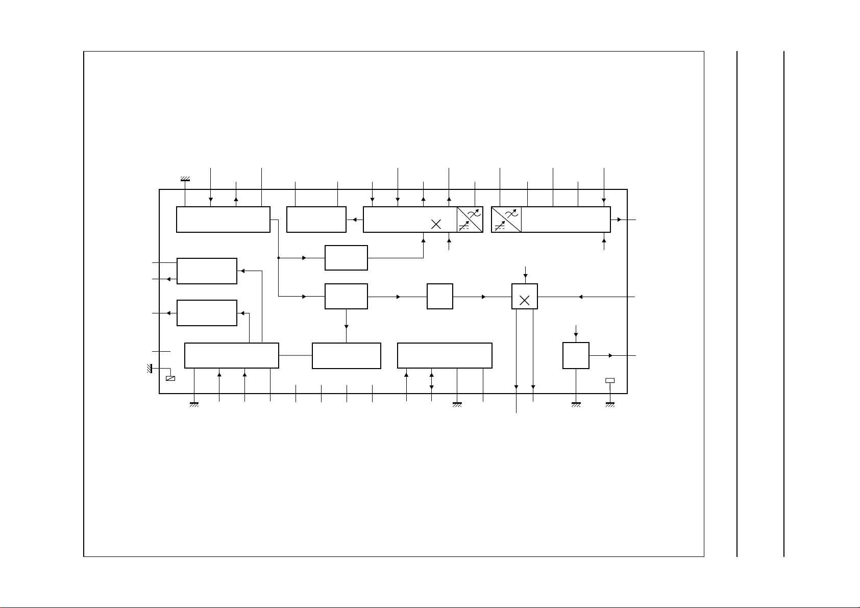
BLOCK DIAGRAM
car radios
Philips Semiconductors Product specification
Front-end and PLL synthesizers for
V
TUNE
CHPOUT
LCKDET
V
CCA2
AGND2
OSCFDB
OSCGND
36 35 37 38 34 32 30 31 11 12 33 27 28 25 24 26
AM/FM
OSCILLATOR
39
CHARGE
40
3
13
14
PUMP
LOCK
DETECTOR
AGND1
f
refNfrefPVCCA1
V
CCOSC
OSCTNK IPIDIO FMRFIP
FMAGC
ref
PIN DIODE
DRIVER
BUFFER
BUFFER
PROGRAMME
DIVIDER N1
n.c. n.c. n.c. n.c. SCL SDA
FMRFIN
FMIFON
I2C-BUS CONTROLPHASE DETECTOR
FMIFOP
FM
AM/FM
N2
FMAGCC
DGND
AMAGCC
V
CCD
AMPREC
AM/FM
AM
159845201023172761
AMMON
AMMOP
AMSB2
AM RF
TEA6810V
TEA6811V
16 21 29
AMPREI
AMSB1
AM/FM
AM/FM
BAND
GAP
AMMGND RFGND
22
18
19
AMPREO
AMMIN
V
ref
MGE727
TEA6810V; TEA6811V
Fig.1 Block diagram.

Philips Semiconductors Product specification
Front-end and PLL synthesizers for
TEA6810V; TEA6811V
car radios
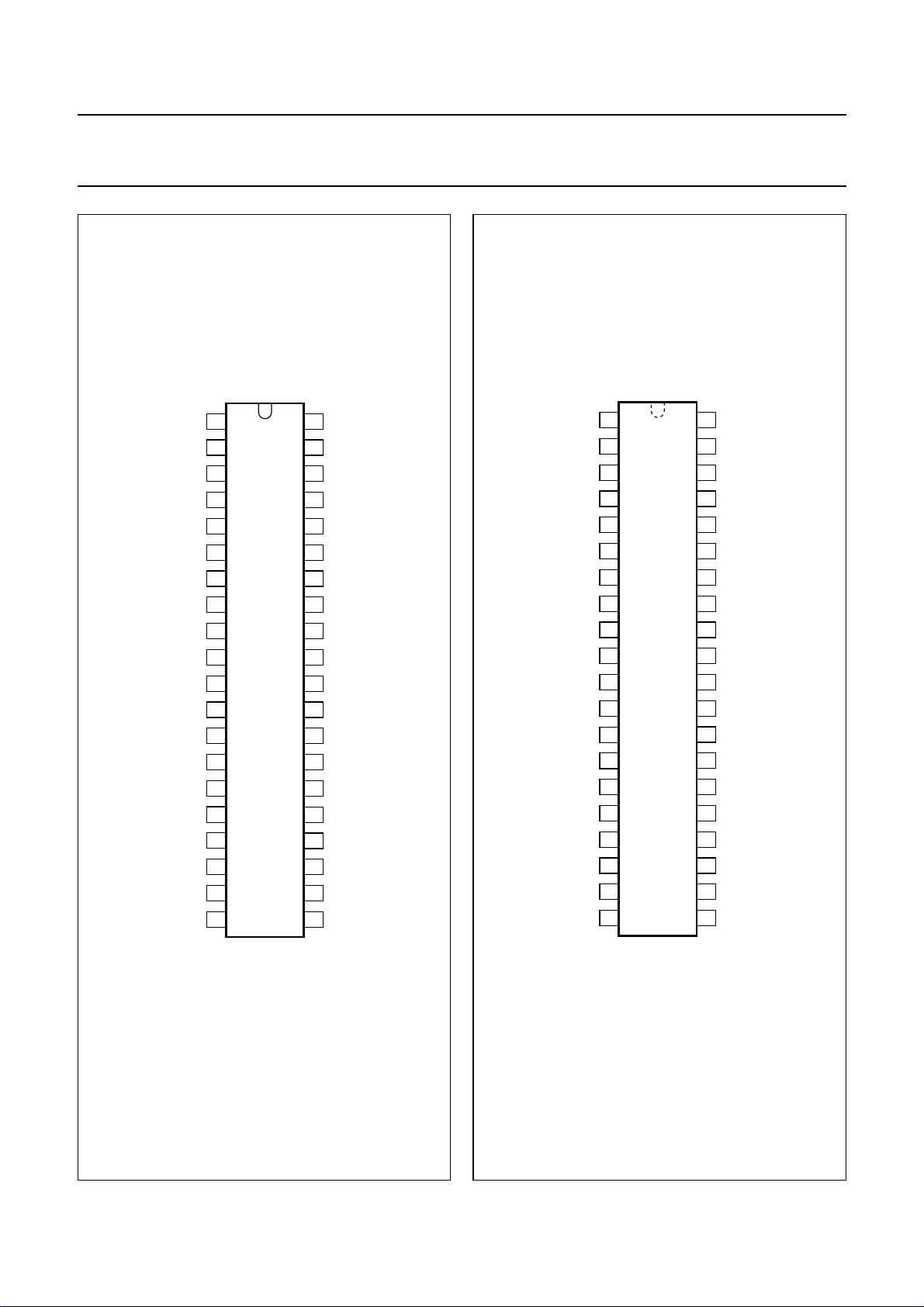
PINNING
(1)
SYMBOL
TEA6810 TEA6811
AGND1 1 1 analog ground 1
V
CCA1
LCKDET 3 3 lock detector flag
SDA 4 4 serial data input/output; I
SCL 5 5 serial clock input; I
f
refN
f
refP
DGND 8 8 digital ground
V
CCD
n.c. 10 10 not connected
FMIFON 11 11 FM mixer negative output (72.2 MHz)
FMIFOP 12 12 FM mixer positive output (72.2 MHz)
V
CCA2
13 13 analog supply voltage 2 (+8.5 V)
AGND2 14 14 analog ground 2
AMMOP 15 15 AM mixer positive output (10.7 MHz)
AMMON 16 16 AM mixer negative output (10.7 MHz)
n.c. 17 17 not connected
AMMIN 18 18 AM mixer RF input
V
ref
19 19 reference voltage output from AM band gap
n.c. 20 20 not connected
AMMGND 21 21 AM mixer ground
AMPREO 22 22 AM preamplifier output
n.c. 23 23 not connected
AMSB1 24 24 AM feedback switch SB1
AMSB2 25 25 AM feedback switch SB2
AMPREI 26 26 AM preamplifier input
AMAGCC 27 27 AM AGC capacitor
AMPREC 28 28 AM preamplifier decoupling capacitor
RFGND 29 29 RF ground
FMRFIP 30 30 RF positive input for FM mixer
FMRFIN 31 31 RF negative input for FM mixer
IPIDIO 32 32 pin diode drive
FMAGCC 33 33 FM AGC integrating capacitor
FMAGC
ref
34 34 FM AGC reference voltage
OSCFDB 35 35 oscillator feedback input
OSCGND 36 36 oscillator ground
OSCTNK 37 37 oscillator tank output
PIN
DESCRIPTION
2 2 analog supply voltage 1 (+5 V)
2
C-bus
2
C-bus
6 6 reference frequency input from TEA6821 N-terminal
7 7 reference frequency input from TEA6821 P-terminal
9 9 digital supply voltage (+5 V)
1996 Jun 18 4

Philips Semiconductors Product specification
Front-end and PLL synthesizers for
car radios
(1)
SYMBOL
V
CCOSC
V
TUNE
CHPOUT 40 40 charge pump output
Note
1. Pins 10, 17, 20 and 23 should be connected to a common ground.
TEA6810 TEA6811
38 38 oscillator supply voltage (+8.5 V)
39 39 tuning voltage
PIN
TEA6810V; TEA6811V
DESCRIPTION
1996 Jun 18 5
Philips Semiconductors Product specification
Front-end and PLL synthesizers for
car radios
handbook, halfpage
AGND1
V
LCKDET
FMIFON
FMIFOP
V
AGND2
AMMOP
AMMON
AMMIN
CCA1
SDA
SCL
f
refN
f
refP
DGND
V
CCD
n.c.
CCA2
n.c.
V
ref
n.c.
1
2
3
4
5
6
7
8
9
10
TEA6810V
11
12
13
14
15
16
17
18
19
20
MGE725
40
39
38
37
36
35
34
33
32
31
30
29
28
27
26
25
24
23
22
21
CHPOUT
V
TUNE
V
CCOSC
OSCTNK
OSCGND
OSCFDB
FMAGC
FMAGCC
IPIDIO
FMRFIN
FMRFIP
RFGND
AMPREC
AMAGCC
AMPREI
AMSB2
AMSB1
n.c.
AMPREO
AMMGND
ref
handbook, halfpage
OSCGND
FMAGC
FMAGCC
AMAGCC
AMPREO
AMMGND
CHPOUT
V
TUNE
V
CCOSC
OSCTNK
OSCFDB
ref
IPIDIO
FMRFIN
FMRFIP
RFGND
AMPREC
AMPREI
AMSB2
AMSB1
n.c.
TEA6810V; TEA6811V
MGE726
1
2
3
4
5
6
7
8
9
10
11
12
13
14
15
16
17
18
19
20
AGND1
V
CCA1
LCKDET
SDA
SCL
f
refN
f
refP
DGND
V
CCD
n.c.
FMIFON
FMIFOP
V
CCA2
AGND2
AMMOP
AMMON
n.c.
AMMIN
V
ref
n.c.
40
39
38
37
36
35
34
33
32
31
TEA6811V
30
29
28
27
26
25
24
23
22
21
Fig.2 Pin configuration (TEA6810).
1996 Jun 18 6
Fig.3 Pin configuration (TEA6811).
Philips Semiconductors Product specification
Front-end and PLL synthesizers for
TEA6810V; TEA6811V
car radios
I2C-BUS ORGANIZATION
The TEA6810V; TEA6811V is controlled via the I2C-bus which is driven from the TEA6821V. For programming purposes
a module address and four data bytes are required. When used partially, the transmission must be ended by a stop
condition.
Table 1 Bit organization
START
S byte 0 A byte 1 A byte 2 A byte 3 A byte 4 A P
Table 2 I
BYTES TO
RECEIVED
(4 BYTES)
Byte 1
program
divider N1
(Low byte)
Byte 2
program
divider N1
(High byte)
Byte 3
switching
Byte 4
testing
MODULE
ADDRESS
2
C-bus address and received bytes
BE
(1)
(1)
MSB LSB
11000100
S7 S6 S5 S4 S3 S2 S1 S0
S15 S14 S13 S12 S11 S10 S9 S8
MSB in-lock
counter
1 = 3-state
0 = normal
charge pump
PROGRAMMABLE
DIVIDER DATA
LSB in-lock
counter
1=f
div
0 = LCKDET
1 = HIGH
0 = LOW
current
tuning
oscillator
1 = test
0 = normal
in-lock
counter
SWITCH
CONTROL
BUS ADDRESS
1 = HIGH
0 = LOW
current
charge
pump
(2)
X
TEST STOP
1=FM
local
0 = FM dx
XX X X
MSB
divider
N2
LSB dividerN21=FM
0=AM
Notes
1. N1 divider ratio is (N + 2); where N is the programmed binary number composed of bytes 1 and 2. For the minimum
ratio; if N < 2048 then N1 divider ratio is {2048 + (N − 2)}.
2. X = don’t care.
Table 3 N2 divider
N2 DIVIDER MSB LSB
300
501
10 1 0
15 1 1
1996 Jun 18 7
Table 4 In-lock
IN-LOCK MSB LSB AM/FM
800FM
16 1 0 AM or FM
32 1 1 AM or FM
48 0 0 AM
64 0 1 AM
Philips Semiconductors Product specification
Front-end and PLL synthesizers for
TEA6810V; TEA6811V
car radios
LIMITING VALUES
In accordance with the Absolute Maximum Rating System (IEC 134).
SYMBOL PARAMETER CONDITIONS MIN. MAX. UNIT
V
CCA1
V
CCA2
V
CCD
V
CCOSC
P
tot
T
stg
V
es
Note
1. Machine model: equivalent to discharging a 200 pF capacitor through 0 Ω.
HANDLING
Inputs and outputs are protected against electrostatic discharge in normal handling. However, to be totally safe, it is
desirable to take normal precautions appropriate to handling MOS devices.
analog supply voltage (pin 2) −0.3 12 V
analog supply voltage (pin 13) −0.3 12 V
digital supply voltage (pin 9) −0.3 12 V
oscillator supply voltage (pin 38) −0.3 12 V
maximum power dissipation − 0.55 W
storage temperature −65 +150 °C
electrostatic handling note 1 −300 +300 V
THERMAL CHARACTERISTICS
SYMBOL PARAMETER VALUE UNIT
R
th j-a
thermal resistance from junction to ambient in free air 90 K/W
DC CHARACTERISTICS
V
13=V38
= 8.5 V; V9=V2= 5.0 V; T
=25°C; unless otherwise specified.
amb
SYMBOL PARAMETER CONDITIONS TYP. MAX. UNIT
I
CCA1
analog input current (pin 2) AM mode 7 9 mA
FM mode 6 8 mA
I
CCA2
analog input current (pin 13) AM mode 17 22 mA
FM mode 15 18 mA
I
CCOSC
oscillator input current (pin 38) AM mode 4 6 mA
FM mode 6 8 mA
I
CCD
digital input current (pin 9) AM mode 32 35 mA
FM mode 27 30 mA
I
AMMO
AM mixer output current (pins 15 and 16) AM mode 8.5 − mA
FM mode 0 − mA
I
FMIFO
FM mixer output current (pins 11 and 12) AM mode 0 − mA
FM mode 10 − mA
1996 Jun 18 8
 Loading...