

Philips TEA6360-V2 Datasheet

DATA SH EET
Preliminary specification
File under Integrated Circuits, IC01
May 1991
INTEGRATED CIRCUITS
TEA6360
5-band stereo equalizer circuit
May 1991 2
Philips Semiconductors Preliminary specification
5-band stereo equalizer circuit TEA6360
FEATURES
• Monolithic integrated 5-band stereo equalizer circuit
• Five filters for each channel
• Centre frequency, bandwidth and maximum boost/cut
defined by external components
• Choise for variable or constant Q-factor via I2C software
• Defeat mode
• All stages are DC-coupled
• I2C-bus control for all functions
• Two different modul addresses programmable.
GENERAL DESCRIPTION
The 5-band stereo equalizer is an 12C-bus controlled tone
processor for application in car radio sets, TV sets and
music centres. It offers the possibility of sound control as
well as equalization of sound pressure behaviour of
different rooms or loudspeakers, especially in cars.
QUICK REFERENCE DATA
ORDERING INFORMATION
Notes
1. SOT232; SOT232-1; 1996 August 08.
2. SOT287; SOT287-1; 1996 August 08.
SYMBOL PARAMETER MIN. TYP. MAX. UNIT
V
p
supply voltage (pin 14) 7 8.5 13.2 V
I
p
supply current − 24.5 − mA
V
1,32
input voltage range − 2.1 to
V
P−1
− V
V
o
maximum output signal level (RMS value, pins 13 and 20) 1.1 − V
G
v
total signal gain, all filters linear −0.5 − 0dB
B −1 dB frequency response (linear) 0 to 20 −−kHz
T
amb
operating ambient temperature −40 − 85 °C
EXTENDED
TYPE NUMBER
PACKAGE
PINS PIN POSITION MATERIAL CODE
TEA6360
(1)
32 shrink DIL plastic SOT232
TEA6360/T
(2)
32 mini-pack plastic SOT287
May 1991 3
Philips Semiconductors Preliminary specification
5-band stereo equalizer circuit TEA6360
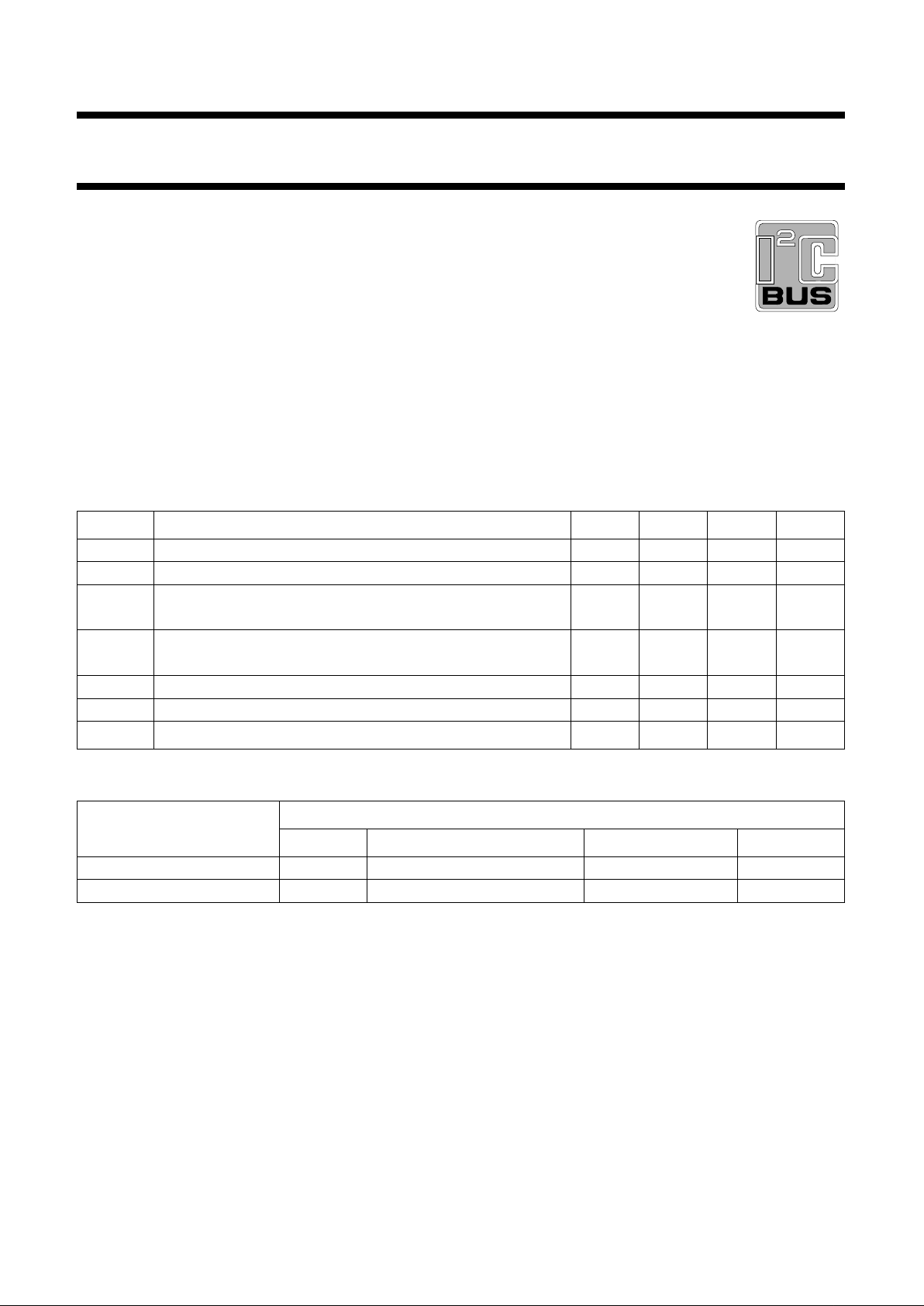
Fig.1 Block diagram, test and application circuit.
May 1991 4
Philips Semiconductors Preliminary specification
5-band stereo equalizer circuit TEA6360
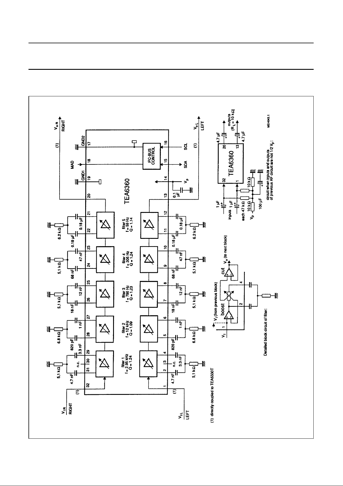
PINNING
SYMBOL PIN DESCRIPTION
V
iL
1 audio frequency input LEFT
F1LA 2 connection A for filter 1 LEFT (f = 2.95 kHz)
n.c. 3 not connected
F1LB 4 connection B for filter 1 LEFT (f = 2.95 kHz)
F2LA 5 connection A for filter 2 LEFT (f = 12 kHz)
F2LB 6 connection B for filter 2 LEFT (f = 12 kHz)
F3LA 7 connection A for filter 3 LEFT (f = 790 Hz)
F3LB 8 connection B for filter 3 LEFT (f = 790 Hz)
F4LA 9 connection A for filter 4 LEFT (f = 205 Hz)
F4LB 10 connection B for filter 4 LEFT (f = 205 Hz)
F5LA 11 connection A for filter 5 LEFT (f = 59 Hz)
F5LB 12 connection B for filter 5 LEFT (f = 59 Hz)
V
oL
13 audio frequency output LEFT
V
P
14 supply voltage (+8.5 V)
SDA 15 I
2
C-bus data line
SCL 16 I
2
C-bus clock line
GND2 17 ground 2 (I
2
C-bus ground)
MAD 18 modul address
GND1 19 ground 1 (analog ground)
V
oR
20 audio frequency output RIGHT
F5RB 21 connection B for filter 5 RIGHT (f = 59 Hz)
F5RA 22 connection A for filter 5 RIGHT (f = 59 Hz)
F4RB 23 connection B for filter 4 RIGHT (f = 205 Hz)
F4RA 24 connection A for filter 4 RIGHT (f = 205 Hz)
F3RB 25 connection B for filter 3 RIGHT (f = 790 Hz)
F3RA 26 connection A for filter 3 RIGHT (f = 790 Hz)
F2RB 27 connection B for filter 2 RIGHT (f = 12 kHz)
F2RA 28 connection A for filter 2 RIGHT (f = 12 kHz)
F1RB 29 connection B for filter 1 RIGHT (f = 2.95 kHz)
n.c. 30 not connected
F1RA 31 connection A for filter 1 RIGHT (f = 2.95 kHz)
V
iR
32 audio frequency input RIGHT
Fig.2 Pin configuration
May 1991 5
Philips Semiconductors Preliminary specification
5-band stereo equalizer circuit TEA6360
FUNCTIONAL DESCRIPTION
The TEA6360 is performed with two stereo channels
(RIGHT and LEFT), each one consists of five equal filter
amplifiers (Fig.1).
The centre frequencies for the different filters as well as
the bandwidth and the control ranges for boost and cut
depend on the external components. Each filter can have
different external components but for one definite pair of
filters the centre frequency as well as the control range for
boost and cut are the same. That means, they have
symmetrical curves for boost and cut.
The control range (maximum value in dB) is divided into
five steps and one extra step for the linear position.
At maximum gain of 12 dB the typical step resolution is
2.4 dB. The internal resistor chain of each filter amplifier is
optimized for 12 dB maximum gain. Therefore the typical
gain factors for 15 dB application are as follows:
The control of the different filters is obtained by selecting
the appropriate subaddress byte (Table 1).
step 1 = 2.7 dB
step 2 = 5.5 dB
step 3 = 8.4 dB
step 4 = 11.6 dB
step 5 = 15.0 dB
The position of the filter in the left channel and that in the
right channel is always the same (stereo).
The position of the boost part and the cut part is
independently controllable (Tables 2 and 3).
The quality factor of the filter has its maximum in the
maximum position (steps 5), if boost (cut on step 0) or cut
(boost on step 0) is used. The quality factor decreases also
with the step number (variable quality factor).
In this mode the control pattern are according to Table 4.
A different control is necessary to achieve a constant
quality factor over the whole control range. For boost with
a constant quality factor over the boost range position +5
is selected and boost control is then performed using cut.
This control technique is applied to the cut range with
position −5 selected and the boost is varied (Table 5).
The cut part has to follow the boost part in each filter for
economic reasons. So the signal is first amplified and then
attenuated. This has to be taken into account for the
internal level diagram in case of constant quality factor.
This may result in a mode between constant Q and
non-constant Q mode; for example for the position +2 it is
not necessary to amplify by step +5 and then attenuate by
−3 step. The combination of step +4 and step −2 to reach
position +2 is a good result (quasi constant quality factor,
Table 6).
LIMITING VALUES
In accordance with the Absolute Maximum System (IEC 134).
Ground pins 19, 28 and 43 connected together.
Note
1. Equivalent to discharging a 200 pF capacitor through a 0 Ω series resistor.
SYMBOL PARAMETER MIN. MAX. UNIT
V
P
supply voltage (pin 14) 0 13.2 V
V
n
voltage on all pins, grounds excluded 0 V
P
V
P
tot
total power dissipation 0 500 mW
T
stg
storage temperature range −40 150 °C
storage temperature range −40 150 °C
T
amb
operating ambient temperature range −40 85 °C
V
ESD
electrostatic handling
(1)
for all pins ±500 V
 Loading...