

Philips TEA6330T Datasheet

INTEGRATED CIRCUITS
DATA SH EET
TEA6330T
Sound fader control circuit
for car radios
Preliminary specification
Supersedes data of June 1991
File under Integrated Circuits, IC01
January 1992
Philips Semiconductors Preliminary specification
Sound fader control circuit
TEA6330T
for car radios
FEATURES
• Stereo/hi-fi processor for car radios performed with
volume, balance, bass and treble controls
• Sound fader control (front/rear) down to −30 dB in steps
of 2 dB
• Fast muting via bus or via setting the muting pin
• Suitable for external audio equalizers, can be looped-in
controlled by the I2C-bus
• Power-on reset on chip sets the device into general
mute position
• AC and DC short-circuit protected concerning
neighbouring pins
• I2C-bus control for all functions.
QUICK REFERENCE DATA
SYMBOL PARAMETER MIN. TYP. MAX. UNIT
V
P
I
P
V
i
V
o
∆G
v
THD total harmonic distortion −− 0.2 %
S/N(W) weighted signal-to-noise ratio − 67 − dB
α
CR
B frequency response (−1 dB) 35 to
supply voltage 7 8.5 10 V
supply current − 26 − mA
maximum AF input signal
(RMS value) 2 −− V
maximum AF output signal
(RMS value) 1.1 −− V
volume control range, separated −66 −+20 dB
fader control range, separated 0 −−30 dB
bass control range −12 −+15 dB
treble control range −12 −+12 dB
crosstalk attenuation − 90 − dB
GENERAL DESCRIPTION
This bipolar IC is an I2C-bus controlled sound/volume
controller for car radios, in addition with fader function and
the possibility of an external equalizer.
− 20000 − Hz
ORDERING INFORMATION
EXTENDED
TYPE NUMBER
TEA6330T
Note
1. Plastic small outline package; 20 leads; body width 7.5 mm; (SOT163A); SOT163-1; 1996 August 02.
January 1992 2
(1)
PINS PIN POSITION MATERIAL CODE
20 SO plastic SOT163A
PACKAGE
Philips Semiconductors Preliminary specification
Sound fader control circuit
for car radios
TEA6330T
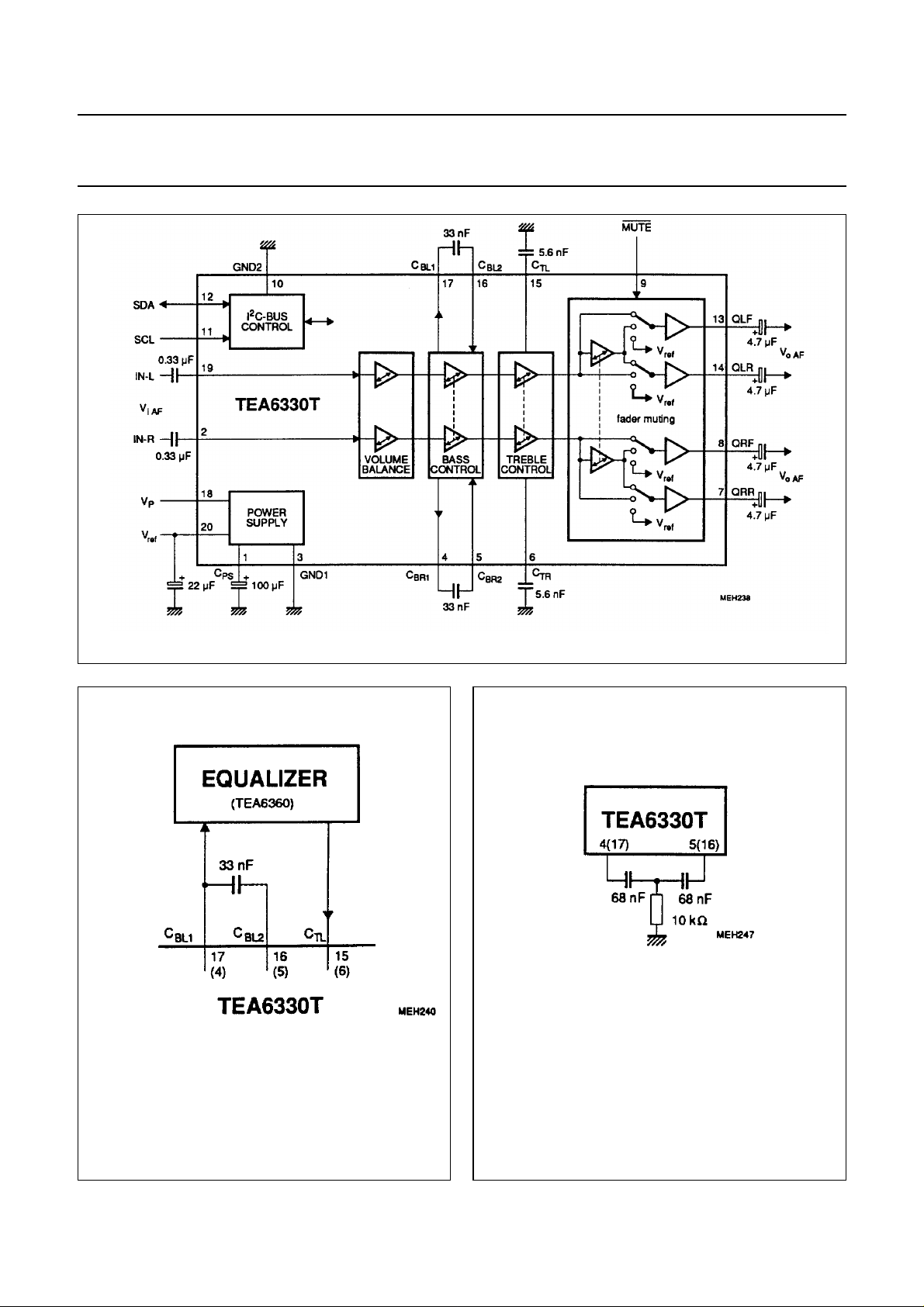
Fig.2 Connection of equalizer (Table 7).
In application with equalizer circuit
TEA6360 coupling capacitors are not
necessary. Connectors for RIGHT in
brackets.
Fig.1 Block and test circuit.
Fig.3 T-filter for enhanced bass control (Fig.5).
Connectors for LEFT in brackets.
January 1992 3
Philips Semiconductors Preliminary specification
Sound fader control circuit
for car radios
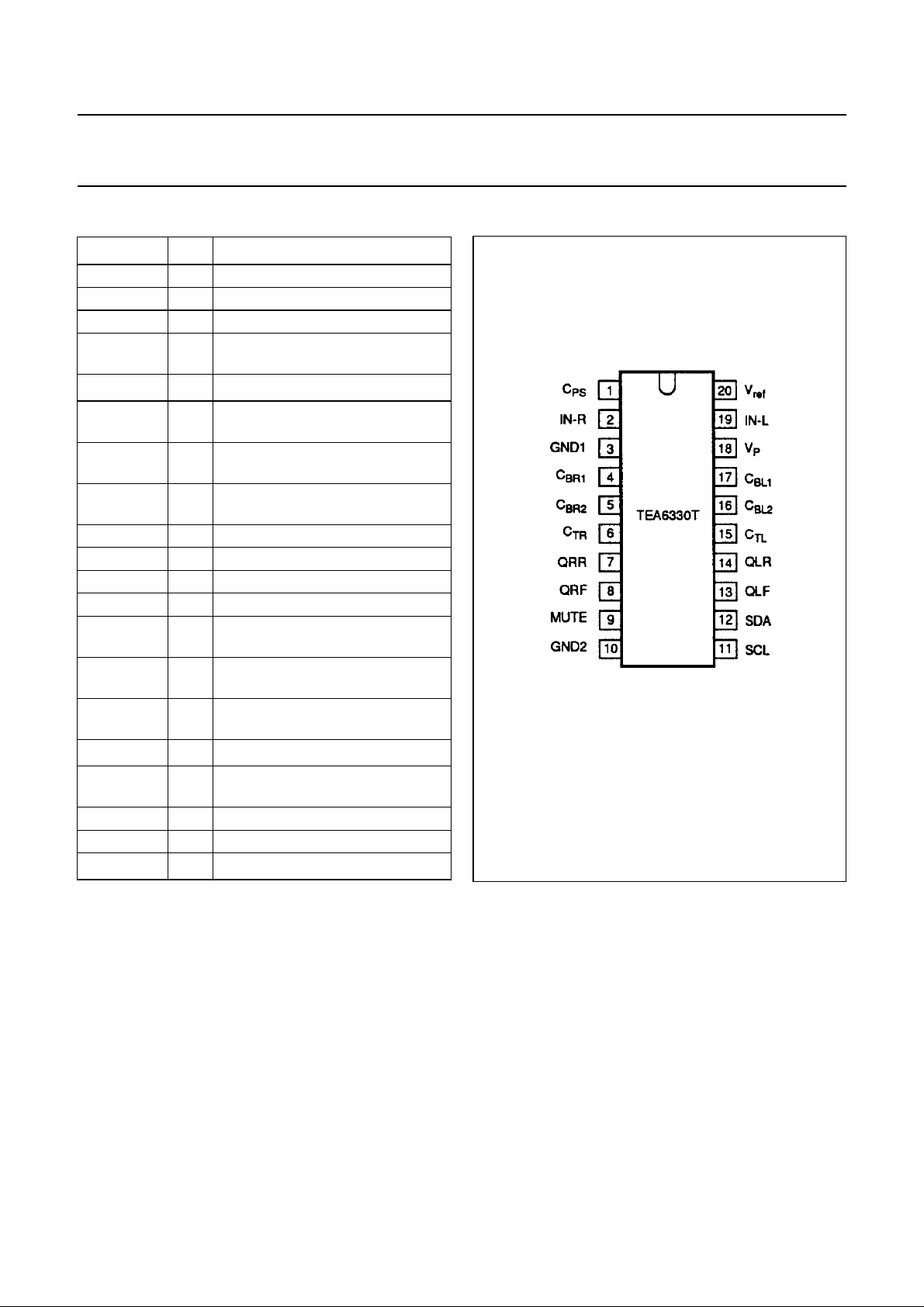
PINNING
SYMBOL PIN DESCRIPTION
C
PS
IN-R 2 audio input signal RIGHT
GND1 3 analog ground (0 V)
C
BR1
C
BR2
C
TR
QRR 7 right audio output signal of rear
QRF 8 right audio output signal of front
MUTE 9 input to set mute externally
GND2 10 digital ground (0 V) for bus control
SCL 11 clock signal of I
SDA 12 data signal of I
QLF 13 left audio output signal of front
QLR 14 left audio output signal of rear
C
TL
C
BL2
C
BL1
V
P
IN-L 19 audio input signal LEFT
V
ref
1 filtering capacitor for power supply
4 capacitor for bass control RIGHT
and signal to equalizer
5 capacitor for bass control RIGHT
6 capacitor for treble control RIGHT,
input signal for equalizer RIGHT
channel
channel
2
C-bus
2
C-bus
channel
channel
15 capacitor for treble control LEFT,
input signal for equalizer LEFT
16 capacitor for bass control LEFT
17 capacitor for bass control LEFT
and signal to equalizer
18 +8.5 V supply voltage
20 reference voltage output (VP/2)
TEA6330T
Fig.4 Pin configuration.
January 1992 4
Philips Semiconductors Preliminary specification
Sound fader control circuit
for car radios
FUNCTIONAL DESCRIPTION
This bipolar IC is an I2C-bus controlled sound/volume
controller for car radios including fader function and the
possibility of an external equalizer. The sound signal
setting is performed by resistor chains in combination with
multi-input operational amplifiers. The advantages of this
principle are the combination of low noise, low distortion
and a high dynamic range. The separated volume controls
of the left and the right channel make the balance control
possible. The value and the characteristic of the balance is
controlled via the I2C-bus.
The contour function is performed by setting an extra bass
control and optional treble, depending on the actual
volume position. Its switching points and its range are also
controllable via the I2C-bus.
An interface is assigned behind the volume control to
loop-in an equalizer (Fig.2). In this case the treble control
is switched off, and the bass control can be used to set the
contour.
TEA6330T
Low level control fader is included independent of the
volume controls, because the TEA6330T has four driver
outputs (for front and rear).
An extra mute position for the front, the rear or for all
channels is built in. The last function may be used for
muting during preset selection. No external interface is
required between the microcomputer and this circuit, for all
switching and controlling functions are controllable via the
two-wire I
The separate mute-pin allows to switch the fader into mute
position without using the I2C-bus.
The on chip power-on reset sets the TEA6330T into the
general mute mode.
2
C-bus.
LIMITING VALUES
In accordance with the Absolute Maximum System (IEC 134). Ground pins 3 and 10 connected together.
SYMBOL PARAMETER MIN. MAX. UNIT
V
P
P
tot
T
stg
T
amb
V
ESD
* Equivalent to discharging a 200 pF capacitor through a 0 Ω series resistor.
** Equivalent to discharging a 100 pF capacitor through a 1.5 kΩ series resistor.
supply voltage (pin 18) 0 10 V
total power dissipation 0 700 mW
storage temperature range −55 150 °C
operating ambient temperature range −40 85 °C
electrostatic handling* for all pins −±300 V
electrostatic handling** for all pins −±4000 V
January 1992 5
Philips Semiconductors Preliminary specification
Sound fader control circuit
TEA6330T
for car radios
CHARACTERISTICS
= 8.5 V; load resistors at audio outputs 10 kΩ, fi = 1 kHz (RS = 600 Ω), bass and treble in linear position, fader in off
V
P
position and T
SYMBOL PARAMETER CONDITIONS MIN. TYP. MAX. UNIT
V
P
I
P
V
ref
V
O
Measurements over all
V
i
V
o
G
v
B frequency response −1 dB roll-off frequency 35 to
α
CR
THD total harmonic distortion f = 20 to 12500 Hz
RR ripple rejection for V
P
N
α
BUS
S/N(W) weighted signal-to-noise ratio for CCIR 468-2 quasi
= 25 °C; measurements taken in Fig.1 unless otherwise specified.
amb
supply voltage range (pin 18) 7 8.5 10 V
supply current − 26 − mA
reference voltage (pin 20) 0.45 VP0.5 V
DC voltage at output (pins 7, 8, 13, 14) − 0.5 V
P
P
0.55 VPV
− V
maximum AF input level for THD = 2 % Gv= −66 to −6 dB
at pins 2 and 19 (RMS value) and V
= 8.1 V 2 −−V
P
maximum AF output level for THD = 2% Gv= −4 to +20 dB
at pins 7, 8, 13, 14 (RMS value) and V
= 8.1 V 1.1 −−V
P
maximum gain by volume setting 19 20 21 dB
− 20000 − Hz
crosstalk attenuation f = 250 to 10000 Hz
= 0 dB 70 90 − dB
G
v
V
V
V
= 50 mV Gv = +20 dB − 0.1 0.3 %
i (RMS)
= 500 mV Gv = 0 dB − 0.05 0.2 %
i (RMS)
= 1.6 V Gv = −10 dB − 0.2 0.5 %
i (RMS)
< 200 mV RMS Gv = 0 dB
R
f = 100 Hz − 70 − dB
f = 40 Hz to 3 kHz − 60 − dB
f = 3 to 12.5 kHz − 50 − dB
noise power at output of a 25 W
powerstage with 26 dB gain
(only contribution of TEA6330T)
mute position
(V9 = 0)
−−10 nW
crosstalk attenuation between SDA, SCL
and signal output Gv = 0 dB − 110 − dB
(20 log V
(p-p)/Vo RMS)
BUS
peak for 6 W power
amplifier
Vi = 50 mV RMS Po = 50 mW − 65 − dB
V
= 500 mV RMS Po = 50 mW − 67 − dB
i
V
= 50 mV RMS Po = 1 W 65 72 − dB
i
V
= 500 mV RMS Po = 1 W 71 78 − dB
i
= 50 mV RMS Po = 6 W; Fig.9 − 72 − dB
V
i
V
= 500 mV RMS Po = 6 W; Fig.9 − 86 − dB
i
January 1992 6
 Loading...