

Philips TEA6320T, TEA6320 Datasheet

INTEGRATED CIRCUITS
DATA SH EET
TEA6320
Sound fader control circuit
Preliminary specification
Supersedes data of September 1992
File under Integrated Circuits, IC01
1995 Dec 19
Philips Semiconductors Preliminary specification
Sound fader control circuit TEA6320
FEATURES
• Source selector for four stereo and one mono inputs
• Interface for noise reduction circuits
• Interface for external equalizer
• Volume, balance and fader control
• Special loudness characteristic automatically controlled
in combination with volume setting
• Bass and treble control
• Mute control at audio signal zero crossing
• Fast mute control via I2C-bus
• Fast mute control via pin
• I2C-bus control for all functions
• Power supply with internal power-on reset.
GENERAL DESCRIPTION
The sound fader control circuit TEA6320 is an I2C-bus
controlled stereo preamplifier for car radio hi-fi sound
applications.
QUICK REFERENCE DATA
SYMBOL PARAMETER CONDITIONS MIN. TYP. MAX. UNIT
V
CC
I
CC
V
o(rms)
G
v
G
step(vol)
G
bass
G
treble
G
step(treble)
(S+N)/N signal-plus-noise to noise ratio V
supply voltage 7.5 8.5 9.5 V
supply current VCC= 8.5 V − 26 − mA
maximum output voltage level VCC= 8.5 V; THD ≤ 0.1% − 2000 − mV
voltage gain −86 − +20 dB
step resolution (volume) − 1 − dB
bass control −15 − +15 dB
treble control −12 − +12 dB
step resolution (bass, treble) − 1.5 − dB
= 2.0 V; Gv= 0 dB;
O
− 105 − dB
unweighted
RR
100
ripple rejection V
< 200 mV; f = 100 Hz;
r(rms)
− 76 − dB
Gv=0dB
α
cs
channel separation 250 Hz ≤ f ≤ 10 kHz; Gv= 0 dB 90 96 − dB
ORDERING INFORMATION
TYPE
NUMBER
NAME DESCRIPTION VERSION
PACKAGE
TEA6320 SDIP32 plastic shrink dual in-line package; 32 leads (400 mil) SOT232-1
TEA6320T SO32 plastic small outline package; 32 leads; body width 7.5 mm SOT287-1
1995 Dec 19 2
Philips Semiconductors Preliminary specification
Sound fader control circuit TEA6320
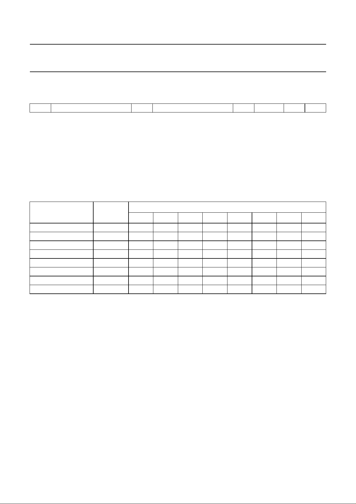
BLOCK DIAGRAM
output
MUTE
output
left
SCL
SDA
right
2.2 kΩ
m
C
33 nF
8.2 nF
5.6 nF 10 nF
150 nF
20 kΩ
220 nF
KVL
C
3
VOLUME II
0 to −55 dB
MUTE
FUNCTION
512
6
7
9
10 8
BALANCE
FADER REAR
DETECTOR
ZERO CROSS
LEFT
TREBLE
LEFT
BASS
VOLUME I
+20 to −31 dB
4
BALANCE
VOLUME II
0 to −55 dB
FADER FRONT
±12 dB
±15 dB
LEFT
LOUDNESS
32
C-BUS
2
I
1
RECEIVER
LOGIC
29
VOLUME II
0 to −55 dB
SOURCE
SELECTOR
BALANCE
FADER FRONT
RIGHT
±12 dB
TREBLE
BASS
RIGHT
±15 dB
RIGHT
VOLUME I
LOUDNESS
+20 to −31 dB
30
BALANCE
VOLUME II
0 to −55 dB
FADER REAR
TEA6320
MED421
150 nF
220 nF
KVL
C
5.6 nF
33 nF
20 kΩ
8.2 nF
handbook, full pagewidth
2.2 kΩ
Fig.1 Block diagram.
28
26 27
24
23 25
POWER
SUPPLY
21
ref
V
100 µF
2
31
CC
V
GND
19
16
15
13
47 µF
9 x 220 nF
input
left
1995 Dec 19 3
source
11
14
22
20
18
17
KIN
C
input
right
input
mono
source
source
Philips Semiconductors Preliminary specification
Sound fader control circuit TEA6320
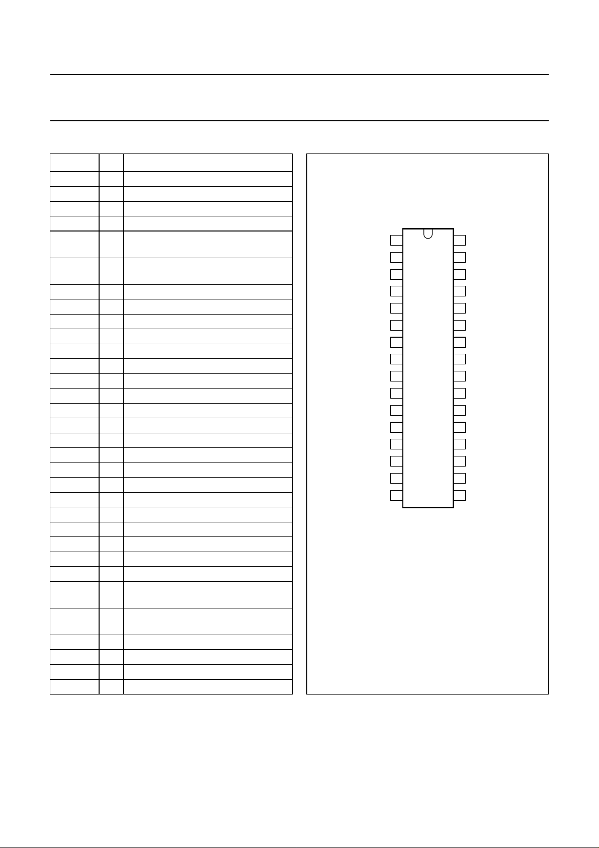
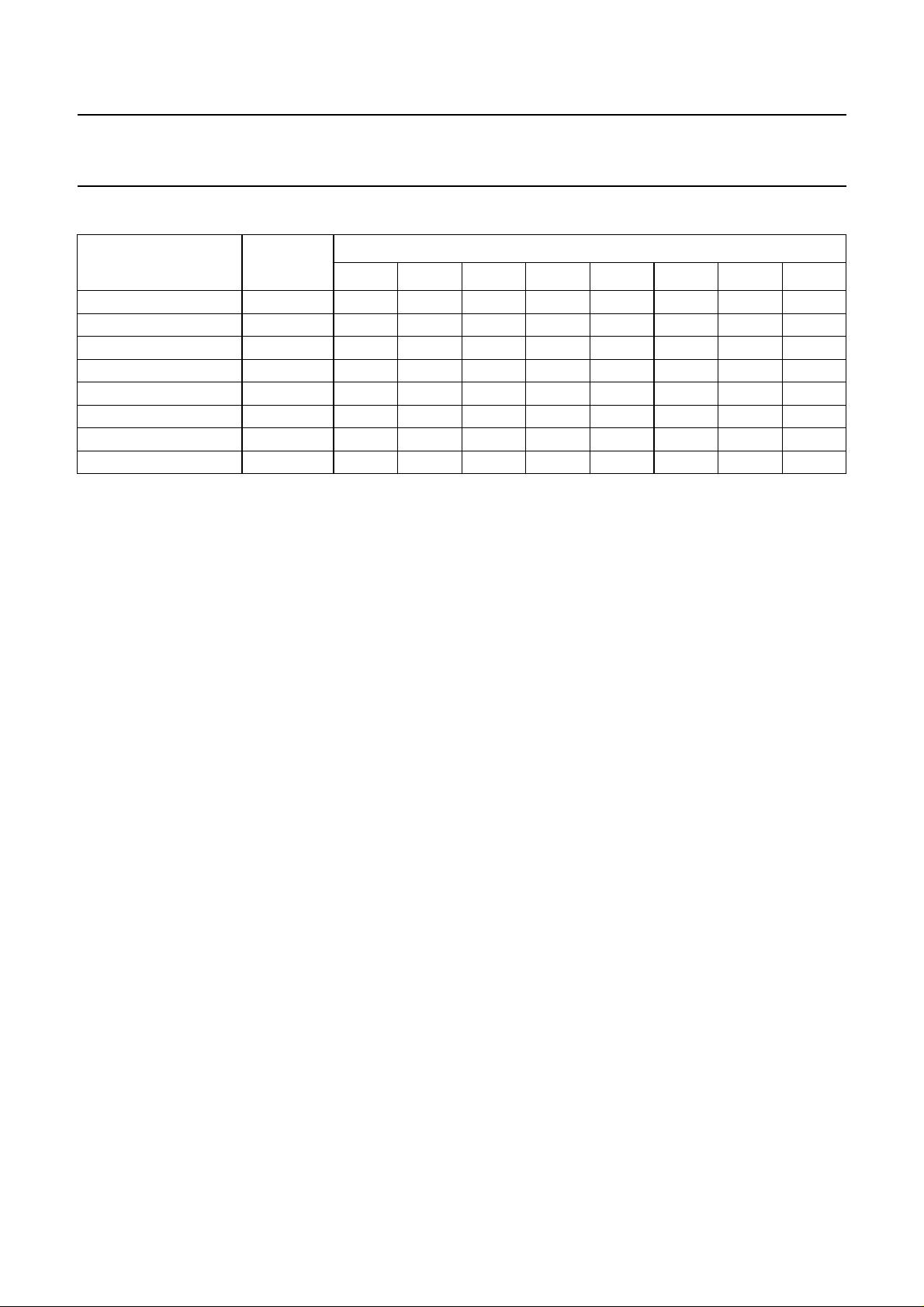
PINNING
SYMBOL PIN DESCRIPTION
SDA 1 serial data input/output
GND 2 ground
OUTLR 3 output left rear
OUTLF 4 output left front
TL 5 treble control capacitor left channel or
input from an external equalizer
B2L 6 bass control capacitor left channel or
output to an external equalizer
B1L 7 bass control capacitor, left channel
IVL 8 input volume I, left control part
ILL 9 input loudness, left control part
QSL 10 output source selector, left channel
IDL 11 input D left source
MUTE 12 mute control
ICL 13 input C left source
IMO 14 input mono source
IBL 15 input B left source
IAL 16 input A left source
IAR 17 input A right source
IBR 18 input B right source
CAP 19 electronic filtering for supply
ICR 20 input C right source
V
ref
21 reference voltage (0.5VCC)
IDR 22 input D right source
QSR 23 output source selector right channel
ILR 24 input loudness right channel
IVR 25 input volume I, right control part
B1R 26 bass control capacitor right channel
B2R 27 bass control capacitor right channel or
output to an external equalizer
TR 28 treble control capacitor right channel
or input from an external equalizer
OUTRF 29 output right front
OUTRR 30 output right rear
V
CC
31 supply voltage
SCL 32 serial clock input
handbook, halfpage
1
SDA
2
GND
OUTLF
TL
B2L
B1L
IVL
ILL
QSL
IDL
MUTE
ICL
IMO
IBL
IAL
3
4
5
6
7
8
9
10
11
12
13
14
15
16
TEA6320
MED422
OUTLR
Fig.2 Pin configuration.
32
31
30
29
28
27
26
25
24
23
22
21
20
19
18
17
SCL
V
CC
OUTRR
OUTRF
TR
B2R
B1R
IVR
ILR
QSR
IDR
V
ref
ICR
CAP
IBR
IAR
1995 Dec 19 4

Philips Semiconductors Preliminary specification
Sound fader control circuit TEA6320
FUNCTIONAL DESCRIPTION
The source selector selects one of 4 stereo inputs or the
mono input. The maximum input signal voltage is
V
= 2 V. The outputs of the source selector and the
i(rms)
inputs of the following volume control parts are available at
pins 8 and 10 for the left channel and pins 23 and 25 for
the right channel. This offers the possibility of interfacing a
noise reduction system.
The volume control function is split into two sections:
volume I control block and volume II control block.
The control range of volume I is between +20 dB and
−31 dB in steps of 1 dB. The volume II control range is
between 0 dB and −55 dB in steps of 1 dB. Although the
theoretical possible control range is 106 dB
(+20 to −86 dB), in practice a range of 86 dB (+20 to
−66 dB) is recommended. The gain/attenuation setting of
the volume I control block is common for both channels.
The volume I control block operates in combination with
the loudness control. The filter is linear when the maximum
gain for the volume I control (+20 dB) is selected. The filter
characteristic increases automatically over a range of
32 dB down to a setting of −12 dB. That means the
maximum filter characteristic is obtained at −12 dB setting
of volume I. Further reduction of the volume does not
further influence the filter characteristic (see Fig.5). The
maximum selected filter characteristic is determined by
external components. The proposed application gives a
maximum boost of 17 dB for bass and 4.5 dB for treble.
The loudness may be switched on or off via I2C-bus control
(see Table 7).
The volume I control block is followed by the bass control
block. A single external capacitor of 33 nF for each
channel in combination with internal resistors, provides the
frequency response of the bass control (see Fig.3). The
adjustable range is between −15 and +15 dB at 40 Hz.
Both loudness and bass control result in a maximum bass
boost of 32 dB for low volume settings.
The treble control block offers a control range between
−12 and +12 dB in steps of 1.5 dB at 15 kHz. The filter
characteristic is determined by a single capacitor of 5.6 nF
for each channel in combination with internal resistors
(see Fig.4).
The basic step width of bass and treble control is 3 dB. The
intermediate steps are obtained by switching 1.5 dB boost
and 1.5 dB attenuation steps.
The bass and treble control functions can be switched off
via I2C-bus. In this event the internal signal flow is
disconnected. The connections B2L and B2R are outputs
and TL and TR are inputs for inserting an external
equalizer.
The last section of the circuit is the volume II block. The
balance and fader functions are performed using the same
control blocks. This is realized by 4 independently
controllable attenuators, one for each output. The control
range of these attenuators is 55 dB in steps of 1 dB with an
additional mute step.
The circuit provides 3 mute modes:
1. Zero crossing mode mute via I
2 independent zero crossing detectors (ZCM,
see Tables 2 and 9 and Fig.16).
2. Fast mute via MUTE pin (see Fig.10).
3. Fast mute via I2C-bus either by general mute (GMU,
see Tables 2 and 9) or volume II block setting
(see Table 4).
The mute function is performed immediately if ZCM is
cleared (ZCM = 0). If the bit is set (ZCM = 1) the mute is
activated after changing the GMU bit. The actual mute
switching is delayed until the next zero crossing of the
audio frequency signal. As the two audio channels (left and
right) are independent, two comparators are built-in to
control independent mute switches.
To avoid a large delay of mute switching when very low
frequencies are processed, the maximum delay time is
limited to typically 100 ms by an integrated timing circuit
and an external capacitor (Cm= 10 nF, see Fig.10). This
timing circuit is triggered by reception of a new data word
for the switch function which includes the GMU bit. After a
discharge and charge period of an external capacitor the
muting switch follows the GMU bit if no zero crossing was
detected during that time.
The mute function can also be controlled externally. If the
mute pin is switched to ground all outputs are muted
immediately (hardware mute). This mute request
overwrites all mute controls via the I2C-bus for the time the
pin is held LOW. The hardware mute position is not stored
in the TEA6320.
For the turn on/off behaviour the following explanation is
generally valid. To avoid AF output caused by the input
signal coming from preceding stages, which produces
output during drop of VCC, the mute has to be set, before
the VCC will drop. This can be achieved by I2C-bus control
or by grounding the MUTE pin.
For use where is no mute in the application before turn off,
a supply voltage drop of more than 1 × VBE will result in a
mute during the voltage drop.
2
C-bus using
1995 Dec 19 5
Philips Semiconductors Preliminary specification
Sound fader control circuit TEA6320
The power supply should include a VCC buffer capacitor,
which provides a discharging time constant. If the input
signal does not disappear after turn off the input will
become audible after certain time. A 4.7 kΩ resistor
discharges the VCC buffer capacitor, because the internal
The hardware mute function is favourable for use in Radio
Data System (RDS) applications. The zero crossing mute
avoids modulation plops. This feature is an advantage for
mute during changing presets and/or sources (e.g. traffic
announcement during cassette playback).
current of the IC does not discharge it completely.
LIMITING VALUES
In accordance with the Absolute Maximum Rating System (IEC 134).
SYMBOL PARAMETER CONDITIONS MIN. MAX. UNIT
V
CC
V
n
supply voltage 0 10 V
voltage at all pins except pin 2
0VCCV
referenced to GND (pin 2)
T
amb
T
stg
V
es
operating ambient temperature −40 +85 °C
storage temperature −65 +150 °C
electrostatic handling note 1
Note
1. Human body model: C = 100 pF; R = 1.5 kΩ; V ≥ 2 kV. Charge device model: C = 200 pF; R = 0 Ω; V ≥ 500 V.
1995 Dec 19 6
Philips Semiconductors Preliminary specification
Sound fader control circuit TEA6320
CHARACTERISTICS
VCC= 8.5 V; RS= 600 Ω; RL=10kΩ; CL= 2.5 nF; AC coupled; f = 1 kHz; T
linear; treble linear; fader off; balance in mid position; loudness off; unless otherwise specified.
SYMBOL PARAMETER CONDITIONS MIN. TYP. MAX. UNIT
V
CC
I
CC
V
DC
supply voltage 7.5 8.5 9.5 V
supply current − 26 33 mA
internal DC voltage at inputs and
outputs
V
ref
G
V
o(rms)
v(max)
internal reference voltage at pin 21 − 4.25 − V
maximum voltage gain RS=0Ω; RL= ∞ 19 20 21 dB
output voltage level for
P
at the power output stage THD ≤ 0.5%; see Fig.11 − 2000 − mV
max
start of clipping THD = 1% 2300 −−mV
R
=2kΩ; CL= 10 nF;
L
THD=1%
V
f
ro
i(rms)
input sensitivity Vo= 2000 mV; Gv=20dB − 200 − mV
roll-off frequency C
= 220 nF;
KIN
C
= 220 nF; Zi=Z
KVL
low frequency (−1 dB) 60 −−Hz
low frequency (−3 dB) 30 −−Hz
high frequency (−1 dB) 20000 −−Hz
C
= 470 nF;
KIN
C
= 100 nF; Zi=Z
KVL
low frequency (−3 dB)
α
cs
channel separation Vi= 2 V; frequency range
250 Hz to 10 kHz
THD total harmonic distortion frequency range
20 Hz to 12.5 kHz
V
= 100 mV; Gv=20dB − 0.1 − %
i
= 1 V; Gv=0dB − 0.05 0.15 %
V
i
V
= 2 V; Gv=0dB − 0.1 − %
i
V
= 2 V; Gv= −10 dB − 0.1 − %
i
RR ripple rejection V
r(rms)
< 200 mV
f = 100 Hz 70 76 − dB
f = 40 Hz to 12.5 kHz − 66 − dB
(S+N)/N signal-plus-noise to noise ratio unweighted;
20 Hz to 20 kHz (RMS);
V
= 2.0 V; see Figs 6 and 7
o
CCIR468-2 weighted; quasi
peak; V
= 2.0 V
o
=0dB − 95 − dB
G
v
=12dB − 88 − dB
G
v
G
=20dB − 81 − dB
v
=25°C; gain control Gv= 0 dB; bass
amb
3.83 4.25 4.68 V
2000 −−mV
i(min)
17 −−Hz
i(typ)
90 96 − dB
− 105 − dB
1995 Dec 19 7
Philips Semiconductors Preliminary specification
Sound fader control circuit TEA6320
SYMBOL PARAMETER CONDITIONS MIN. TYP. MAX. UNIT
P
no(rms)
α
ct
Source selector
Z
i
α
S
V
i(rms)
V
offset
Z
o
R
L
C
L
G
v
Control part (source selector disconnected; source resistance 600 Ω)
Z
i
Z
o
R
L
C
L
R
DCL
V
i(rms)
V
no
CR
tot
G
step
noise output power (RMS value)
mute position; note 1 −−10 nW
only contribution of TEA6320;
power amplifier for 6 W
crosstalk
V
20
bus p p–()
-------------------------- -log
V
o rms()
between bus
note 2 − 110 − dB
inputs and signal outputs
input impedance 25 35 45 kΩ
input isolation of one selected
source to any other input
maximum input voltage
(RMS value)
DC offset voltage at source
f = 1 kHz − 105 − dB
f = 12.5 kHz − 95 − dB
THD < 0.5%; VCC= 8.5 V − 2.15 − V
THD < 0.5%; V
= 7.5 V − 1.8 − V
CC
−−10 mV
selector output by selection of any
inputs
output impedance − 80 120 Ω
output load resistance 10 −−kΩ
output load capacity 0 − 2500 pF
voltage gain, source selector − 0 − dB
input impedance volume input 100 150 200 kΩ
input impedance loudness input 25 33 40 kΩ
output impedance − 80 120 Ω
output load resistance 2 −−kΩ
output load capacity 0 − 10 nF
DC load resistance at output to
4.7 −−kΩ
ground
maximum input voltage
THD < 0.5% − 2.15 − V
(RMS value)
noise output voltage CCIR468-2 weighted; quasi
peak
G
=20dB − 110 220 µV
v
G
=0dB − 33 50 µV
v
G
= −66 dB − 13 22 µV
v
mute position − 10 −µV
total continuous control range − 106 − dB
recommended control range − 86 − dB
step resolution − 1 − dB
step error between any adjoining
−−0.5 dB
step
1995 Dec 19 8
Philips Semiconductors Preliminary specification
Sound fader control circuit TEA6320
SYMBOL PARAMETER CONDITIONS MIN. TYP. MAX. UNIT
∆G
a
∆G
t
MUTE
att
V
offset
Volume I control and loudness
CR
vol
G
v
G
step
L
Bmax
attenuator set error Gv= +20 to −50 dB −−2dB
G
=−51 to −66 dB −−3dB
v
gain tracking error Gv= +20 to −50 dB −−2dB
mute attenuation see Fig.10 100 110 − dB
DC step offset between any
adjoining step
DC step offset between any step to
Gv=0to−66 dB − 0.2 10 mV
G
=20to0dB − 215mV
v
=0to−66 dB −−10 mV
G
v
mute
continuous volume control range − 51 − dB
voltage gain −31 − +20 dB
step resolution − 1 − dB
maximum loudness boost loudness on; referred to
loudness off; boost is
determined by external
components
f = 40 Hz − 17 − dB
f = 10 kHz − 4.5 − dB
Bass control
G
bass
bass control, maximum boost f = 40 Hz 14 15 16 dB
maximum attenuation f = 40 Hz 14 15 16 dB
G
step
step resolution (toggle switching) f = 40 Hz − 1.5 − dB
step error between any adjoining
step
V
offset
DC step offset in any bass position −−20 mV
Treble control
G
treble
treble control, maximum boost f = 15 kHz 11 12 13 dB
maximum attenuation f = 15 kHz 11 12 13 dB
maximum boost f > 15 kHz −−15 dB
G
step
step resolution (toggle switching) f = 15 kHz − 1.5 − dB
step error between any adjoining
step
V
offset
DC step offset in any treble
position
Volume II, balance and fader control
CR continuous attenuation fader and
volume control range
G
step
step resolution − 12dB
attenuation set error −−1.5 dB
f = 40 Hz −−0.5 dB
f = 15 kHz −−0.5 dB
−−10 mV
53.5 55 56.5 dB
1995 Dec 19 9
Philips Semiconductors Preliminary specification
Sound fader control circuit TEA6320
SYMBOL PARAMETER CONDITIONS MIN. TYP. MAX. UNIT
Mute function (see Fig.10)
H
ARDWARE MUTE
V
sw
mute active
V
swLOW
I
i
mute passive: level internally defined
V
swHIGH
t
d(mute)
ZERO CROSSING MUTE
I
d
I
ch
V
swDEL
t
d
V
wind
mute switch level (2 × VBE) − 1.45 − V
input level −−1.0 V
input current V
=1V −300 −−µA
swLOW
saturation voltage −−VCCV
delay until mute passive −−0.5 ms
discharge current 0.3 0.6 1.2 µA
charge current −300 −150 −µA
delay switch level (3 × VBE) − 2.2 − V
delay time Cm=10nF − 100 − ms
window for audio signal zero
− 30 40 mV
crossing detection
Muting at power supply drop
V
CCdrop
supply drop for mute active − V19−
− V
0.7
2
Power-on reset (when reset is active the GMU-bit (general mute) is set and the I
C-bus receiver is in
reset position)
V
CC
increasing supply voltage start of
−−2.5 V
reset
end of reset 5.2 6.5 7.2 V
decreasing supply voltage start of
4.2 5.5 6.2 V
reset
Digital part (I
V
iH
V
iL
I
iH
I
iL
V
oL
2
C-bus pins); note 3
HIGH level input voltage 3 − 9.5 V
LOW level input voltage −0.3 − +1.5 V
HIGH level input current −10 − +10 µA
LOW level input current −10 − +10 µA
LOW level output voltage IL=3mA −−0.4 V
Notes to the characteristics
1. The indicated values for output power assume a 6 W power amplifier at 4 Ω with 20 dB gain and a fixed attenuator
of 12 dB in front of it. Signal-to-noise ratios exclude noise contribution of the power amplifier.
2. The transmission contains: total initialization with MAD and subaddress for volume and 8 data words, see also
definition of characteristics, clock frequency = 50 kHz, repetition burst rate = 400 Hz, maximum bus signal
amplitude = 5 V (p-p).
3. The AC characteristics are in accordance with the I2C-bus specification. This specification,
use it
”, can be ordered using the code 9398 393 40011.
“The I2C-bus and how to
1995 Dec 19 10
Philips Semiconductors Preliminary specification
Sound fader control circuit TEA6320
I2C-BUS PROTOCOL
2
C-bus format
I
(1)
S
SLAVE ADDRESS
Notes
1. S = START condition.
2. SLAVE ADDRESS (MAD) = 1000 0000.
3. A = acknowledge, generated by the slave.
4. SUBADDRESS (SAD), see Table 1.
5. DATA, see Table 1; if more than 1 byte of DATA is transmitted, then auto-increment of the significant subaddress is
performed.
6. P = STOP condition.
Table 1 Second byte after MAD
(2)
(3)
A
SUBADDRESS
(4)
(3)
A
DATA
(5)
(3)
A
(6)
P
FUNCTION BIT
765432
(1)
(1)
1
(1)
0
Volume/loudness V 00000000
Fader front right FFR 00000001
Fader front left FFL 00000010
Fader rear right FRR 00000011
Fader rear left FRL 00000100
Bass BA 00000101
Treble TR 00000110
Switch S 00000111
Note
1. Significant subaddress.
MSB LSB
1995 Dec 19 11
Philips Semiconductors Preliminary specification
Sound fader control circuit TEA6320
Table 2 Definition of third byte after MAD and SAD
FUNCTION BIT
MSB LSB
76543210
Volume/loudness V ZCM
Fader front right FFR X
Fader front left FFL X
Fader rear right FRR X
Fader rear left FRL X
Bass BA X
Treble TR X
(4)
(4)
(4)
(4)
(4)
(4)
Switch S GMU
Notes
1. Zero crossing mode.
2. Switch loudness on/off.
3. Volume control.
4. Don’t care bits (logic 1 during testing).
5. Fader control front right.
6. Fader control front left.
7. Fader control rear right.
8. Fader control rear left.
9. Bass control.
10. Treble control.
11. Mute control for all outputs (general mute).
12. Source selector control.
(1)
(11)
LOFF
(4)
X
(4)
X
(4)
X
(4)
X
(4)
X
(4)
X
(4)
X
(2)
V5
FFR5
FFL5
FRR5
FRL5
(4)
X
(4)
X
(4)
X
(3)
(6)
(8)
(5)
(7)
V4
FFR4
FFL4
FRR4
FRL4
BA4
TR4
(4)
X
(3)
(9)
(10)
(6)
(8)
(5)
(7)
V3
FFR3
FFL3
FRR3
FRL3
BA3
TR3
(4)
X
(3)
(9)
(10)
(6)
(5)
(8)
(7)
V2
FFR2
FFL2
FRR2
FRL2
BA2
TR2
SC2
(3)
(9)
(10)
(12)
(6)
(5)
(8)
(7)
V1
FFR1
FFL1
FRR1
FRL1
BA1
TR1
SC1
(3)
(10)
(12)
(9)
(6)
(8)
(5)
(7)
V0
FFR0
FFL0
FRR0
FRL0
BA0
TR0
SC0
(3)
(5)
(6)
(7)
(8)
(9)
(10)
(12)
1995 Dec 19 12
 Loading...