

Philips TEA6300T, TEA6300 Datasheet

INTEGRATED CIRCUITS
DATA SH EET
TEA6300
TEA6300T
Sound fader control circuit
Product specification
File under Integrated Circuits, IC01
May 1990
Philips Semiconductors Product specification
Sound fader control circuit
GENERAL DESCRIPTION
The Sound Fader Control circuit (SOFAC) is an I2C-bus
controlled preamplifier for car radios.
Features
• Source selector for three stereo inputs
• Inputs and outputs for noise reduction circuits
• Volume and balance control; control range of 86 dB in
steps of 2 dB
• Bass and treble control from + 15 dB (treble 12 dB)
to −12 dB in steps of 3 dB
• Fader control from 0 dB to −30 dB in steps of 2 dB
• Fast muting
• Low noise suitable for DOLBY* B and C NR (noise
reduction)
• Signal handling suitable for compact disc
2
• I
C-bus control for all functions
• ESD protected
TEA6300
TEA6300T
QUICK REFERENCE DATA
SYMBOL PARAMETER MIN. TYP. MAX. UNIT
V
V
V
f
r
α
CC
i(rms)
i(rms)
CS
Supply voltage 7,0 8,5 13,2 V
Input sensitivity for full power at the output stage − 50 − mV
Input signal handling − 1,65 − V
Frequency response 35 − 20 000 Hz
Channel separation; f = 250 Hz to 10 kHz 70 92 − dB
THD Total harmonic distortion − 0,05 − %
(S+N)/N Signal plus noise-to-noise ratio − 80 − dB
T
amb
Operating ambient temperature range −40 −+ 85 °C
* Dolby is a registered trademark of Dolby Laboratories Licensing Corporation, San Francisco, California (U.S.A.).
PACKAGE OUTLINES
28-lead dual in-line; plastic (SOT117); SOT117-1; 1996 August 15.
28-lead mini-pack; plastic (SO28; SOT136A); SOT136-1; 1996 August 15.
May 1990 2
This text is here in white to force landscape pages to be rotated correctly when browsing through the pdf in the Acrobat reader.This text is here in
_white to force landscape pages to be rotated correctly when browsing through the pdf in the Acrobat reader.This text is here inThis text is here in
white to force landscape pages to be rotated correctly when browsing through the pdf in the Acrobat reader. white to force landscape pages to be ...
May 1990 3
Philips Semiconductors Product specification
Sound fader control circuit
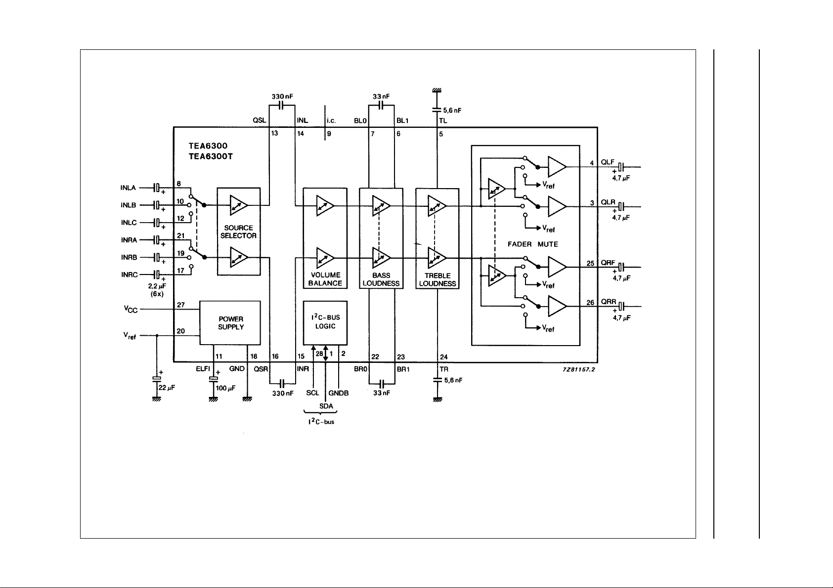
Fig.1 Block diagram.
TEA6300T
TEA6300
Philips Semiconductors Product specification
Sound fader control circuit
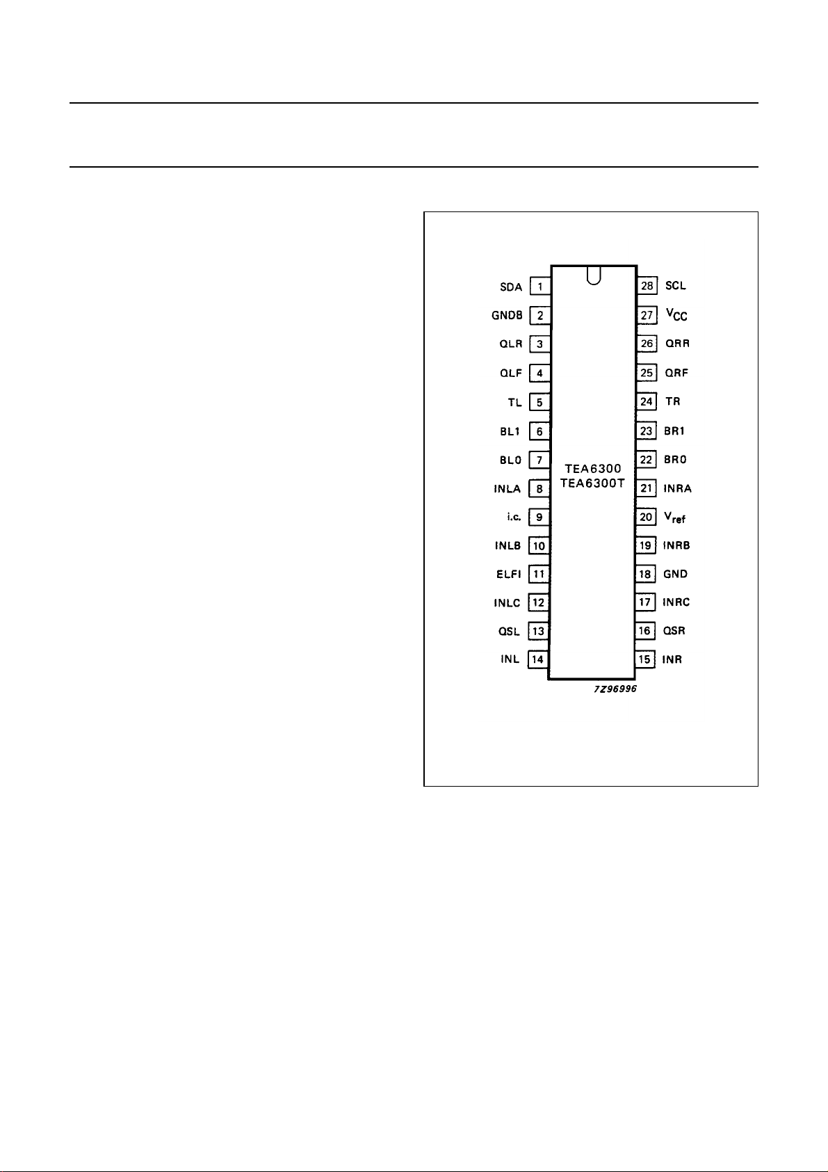
PINNING
2
2
C-bus)
C-bus)
1 SDA serial data input/output (I
2
2 GNDB ground for I
3 QLR output left rear
4 QLF output left front
5 TL treble control capacitor; left channel
6 BL1 bass control capacitor; left channel
7 BL0 bass control capacitor; left channel
8 INLA input left source A
9 i.c. internally connected
10 INLB input left source B
11 ELFI electronic filtering for supply
12 INLC input left source C
13 QSL output source selector left
14 INL input left control part
15 INR input right control part
16 QSR output source selector right
17 INRC input right source C
18 GND ground
19 INRB input right source B
20 V
21 INRA input right source A
22 BRO bass control capacitor; right channel
23 BR1 bass control capacitor; right channel
24 TR treble control capacitor; right channel
25 QRF output right front
26 QRR output right rear
27 V
28 SCL serial clock input (I
reference voltage (1/2 VCC)
ref
supply voltage
CC
C-bus terminals
TEA6300
TEA6300T
Fig.2 Pinning diagram.
May 1990 4

Philips Semiconductors Product specification
Sound fader control circuit
TEA6300
TEA6300T
FUNCTIONAL DESCRIPTION
The source selector selects three stereo channels −RF part (AM/FM), recorder and compact disc. As the outputs of the
source selector and the inputs of the main control part are available, additional circuits such as compander and equalizer
systems may be inserted into the signal path. The AC signal setting is performed by resistor chains in combination with
multi-input operational amplifiers. The advantage of this principle is the combination of low noise, low distortion and a
high dynamic range for the circuit.
The separate volume controls of the left and the right channel facilitate correct balance control. The range and balance
control is software programmable.
Because the TEA6300 has four outputs a low-level fader is included. The fader control is independent of the volume
control and an extra mute position is built in for the front, the rear or for all channels. The last function may be used for
muting during preset selection. An extra pop suppression circuit is built in for pop-free switching on and off. As all
switching and control functions are controllable via the two-wire I
microcomputer and the TEA6300 is required.
The on-chip power-on-reset sets the TEA6300 to the general mute mode.
RATINGS
Limiting values in accordance with the Absolute Maximum System (IEC 134)
SYMBOL PARAMETER MIN. MAX. UNIT
V
CC
P
tot
T
stg
T
amb
Supply voltage (pin 27-18) − 16 V
Maximum power dissipation − 1W
Storage temperature range −55 +150 °C
Operating ambient temperature range −40 + 85 °C
2
C-bus, no external interface between the
May 1990 5

Philips Semiconductors Product specification
Sound fader control circuit
CHARACTERISTICS
V
= 8,5 V; RS = 600 Ω; RL = 10 kΩ; f = 1 kHz; T
CC
SYMBOL PARAMETER MIN. TYP. MAX. UNIT
V
CC
I
CC
I
CC
I
CC
V
DC
V
REF
G
v
V
o(rms)
V
o(rms)
V
i(rms)
f
r
α
CS
THD V
THD V
THD V
RR
100
RR
range
Supply voltage 7,0 8,5 13,2 V
Supply current − 26 − mA
Supply current at 8,5 V −−33 mA
Supply current at 13,2 V −−44 mA
DC voltage
inputs, outputs and reference 0,45 0,5 0,55 V
Internal reference voltage (pin 20)
V
= 0,5 V
ref
CC
Maximum voltage gain
bass and treble linear, fader off 19 20 21 dB
Output voltage level
for P
at the output stage − 500 − mV
max
for start of clipping − 1000 − mV
Input sensitivity
at Vo = 500 mV − 50 − mV
Frequency response
bass and treble linear; roll-off
frequency −1 dB 35 − 20 000 Hz
Channel separation
G
= 0 dB; bass and treble linear;
v
frequency range 250 Hz to 10 kHz 70 92 − dB
Total harmonic distortion
frequency range 20 Hz to 12,5 kHz
= 50 mV; Gv= 20 dB − 0,1 0,3 %
i
= 500 mV; Gv = 0 dB − 0,05 0,2 %
i
= 1,6 V; Gv= −10 dB − 0,2 0,5 %
i
Ripple rejection
V
< 200 mV; Gv = 0 dB;
r(rms)
bass and treble linear;
at f = 100 Hz − 70 − dB
at f = 40 Hz to 12,5 kHz − 60 − dB
= 25 °C; test circuit Fig.10; unless otherwise specified
amb
− 4,25 − V
TEA6300
TEA6300T
CC
May 1990 6

Philips Semiconductors Product specification
Sound fader control circuit
TEA6300
TEA6300T
SYMBOL PARAMETER MIN. TYP. MAX. UNIT
Signal plus noise-to-noise ratio
bass and treble linear; notes 1 and 2
CCIR 468-2 weighted; quasi peak
(S + N)/N V
(S + N)/N V
(S + N)/N V
(S + N)/N V
(S + N)/N V
(S + N)/N V
P
no
α
B
Source selector
Z
i
Z
o
R
L
C
L
α
S
G
v
V
b int/Vref
V
i(rms)
V
i(rms)
THD Vi= 500 mV; RL= 10 kΩ−−0,1 %
V
no
V
o
= 50 mV; Vo= 46 mV; Po= 50 mW − 65 − dB
i
= 500 mV; Vo= 45 mV; Po= 50 mW − 67 − dB
i
= 50 mV; Vo= 200 mV; Po= 1 W 65 70 − dB
i
= 500 mV; Vo= 200 mV; Po= 1 W 65 78 − dB
i
= 50 mV; Vo= 500 mV; Po= 6 W − 70 − dB
i
= 500 mV; Vo= 500 mV; Po= 6 W − 85 − dB
i
Noise output power
mute position, only contribution of
TEA6300; power amplifier for 25 W −−10 nW
Crosstalk (20 log V
bus(p-p)/Vo(rms)
)
between bus inputs and signal outputs
GV= 0 dB; bass and treble linear − 110 − dB
Input impedance 20 30 40 kΩ
Output impedance −−100 Ω
Output load resistance 10 −−kΩ
Output load capacity 0 − 200 pF
Input isolation
not selected source; frequency range
40 Hz to 12,5 kHz − 80 − dB
Voltage gain
RL≥ 10 kΩ−0−dB
Internal bias voltage ratio − 1 −
Maximum input voltage level (RMS value)
THD < 0,5% − 1,65 − V
THD < 0,5%; VCC= 7,5 V − 1,5 − V
Total harmonic distortion
Noise output voltage
weighted CCIR 468-2, quasi peak − 920µV
DC offset voltage
between any inputs −−10 mV
May 1990 7
 Loading...