

Philips TEA5768HL Datasheet

34.807IRELESS
34.807IRELESS
IMPORTANT NOTICE
Dear customer,
nd
As from August 2
ST-NXP Wireless.
As a result, the following changes are applicable to the attached document.
● Company name - Philips Semiconductors is replaced with ST-NXP Wireless.
2008, the wireless operations of NXP have moved to a new company,
● Copyright - the copyright notice at the bottom of each page “© Koninklijke Philips
Electronics N.V. 200x. All rights reserved”, shall now read: “© ST-NXP Wireless 200x All rights reserved”.
● Web site - http://www.semiconductors.philips.com is replaced with
http://www.stnwireless.com
● Contact information - the list of sales offices previously obtained by sending an email
to sales.addresses@www.semiconductors.philips.com
http://www.stnwireless.com
If you have any questions related to the document, please contact our nearest sales office.
Thank you for your cooperation and understanding.
ST-NXP Wireless
under Contacts.
, is now found at
www.stnwireless.com
INTEGRATED CIRCUITS
DATA SH EET
TEA5768HL
Low-power FM stereo radio for
handheld applications
Product specification
Supersedes data of 2003 Nov 06
2004 Sep 13

Philips Semiconductors Product specification
Low-power FM stereo radio for
handheld applications
CONTENTS
1 FEATURES
2 GENERAL DESCRIPTION
3 ORDERING INFORMATION
4 QUICK REFERENCE DATA
5 BLOCK DIAGRAM
6 PINNING
7 FUNCTIONAL DESCRIPTION
7.1 Low-noise RF amplifier
7.2 FM mixer
7.3 VCO
7.4 Crystal oscillator
7.5 PLL tuning system
7.6 RF AGC
7.7 IF filter
7.8 FM demodulator
7.9 Level voltage generator and analog-to-digital
converter
7.10 IF counter
7.11 Soft mute
7.12 MPX decoder
7.13 Signal dependent mono to stereo blend
7.14 Signal dependent AF response
7.15 Software programmable ports
8I
8.1 I2C-bus specification
8.1.1 Data transfer
8.1.2 Power-on reset
8.2 I2C-bus protocol
8.3 Writing data
8.4 Reading data
8.5 Bus timing
2
C-BUS AND BUS-CONTROLLED
FUNCTIONS
TEA5768HL
9 LIMITING VALUES
10 THERMAL CHARACTERISTICS
11 DC CHARACTERISTICS
12 AC CHARACTERISTICS
13 INTERNAL PIN CONFIGURATION
14 APPLICATION INFORMATION
15 PACKAGE OUTLINE
16 SOLDERING
16.1 Introduction to soldering surface mount
packages
16.2 Reflow soldering
16.3 Wave soldering
16.4 Manual soldering
16.5 Suitability of surface mount IC packages for
wave and reflow soldering methods
17 DATA SHEET STATUS
18 DEFINITIONS
19 DISCLAIMERS
20 PURCHASE OF PHILIPS I2C COMPONENTS
2004 Sep 13 2
Philips Semiconductors Product specification
Low-power FM stereo radio for
handheld applications
1 FEATURES
• High sensitivity due to integrated low-noise RF input
amplifier
• FM mixer for conversion to IF of the US/Europe
(87.5 MHz to 108 MHz) and Japanese
(76 MHz to 91 MHz) FM band
• Preset tuning to receive Japanese TV audio up to
108 MHz
• RF Automatic Gain Control (AGC) circuit
• LC tuner oscillator operating with low cost fixed chip
inductors
• FM IF selectivity performed internally
• No external discriminator neededdue to fully integrated
FM demodulator
• Crystal reference frequency oscillator; the oscillator
operates with a 32.768 kHz clock crystal or with a
13 MHz crystal and with an externally applied 6.5 MHz
reference frequency
• PLL synthesizer tuning system
• I2C-bus
• 7-bit IF counter output via the I2C-bus
• 4-bit level information output via the I2C-bus
• Soft mute
• Signal dependent mono to stereo blend [Stereo Noise
Cancelling (SNC)]
• Signal dependent High Cut Control (HCC)
TEA5768HL
• Soft mute, SNC and HCC can be switched off via the
I2C-bus
• Adjustment-free stereo decoder
• Autonomous search tuning function
• Standby mode
• Two software programmable ports
• Bus enable line to switch the bus input and output lines
into 3-state mode.
2 GENERAL DESCRIPTION
The TEA5768HL is a single-chip electronically tuned FM
stereo radio for low-voltage applications with fully
integrated IF selectivity and demodulation. The radio is
completely adjustment-free and only requires a minimum
of small and low cost external components. The radio can
be tuned to the European, US and Japanese FM bands.
3 ORDERING INFORMATION
TYPE
NUMBER
TEA5768HL LQFP32 plastic low profile quad flat package; 32 leads; body 7 × 7 × 1.4 mm SOT358-1
2004 Sep 13 3
NAME DESCRIPTION VERSION
PACKAGE
Philips Semiconductors Product specification
Low-power FM stereo radio for
TEA5768HL
handheld applications
4 QUICK REFERENCE DATA
V
CCA=VCC(VCO)=VCCD
SYMBOL PARAMETER CONDITIONS MIN. TYP. MAX. UNIT
V
CCA
V
CC(VCO)
analog supply voltage 2.5 3.0 5.0 V
voltage controlled oscillator
supply voltage
V
CCD
I
CCA
I
CC(VCO)
digital supply voltage 2.5 3.0 5.0 V
analog supply current operating; V
voltage controlled oscillator
supply current
I
CCD
f
FM(ant)
T
amb
digital supply current operating; V
FM input frequency 76 − 108 MHz
ambient temperature V
FM overall system parameters; see Fig.5
V
S
S
RF
−200
+200
RF sensitivity input voltage fRF= 76 MHz to 108 MHz; ∆f = 22.5 kHz;
LOW side 200 kHz selectivity ∆f=−200 kHz; fRF= 76 MHz to 108 MHz;
HIGH side 200 kHz
selectivity
V
AFL
; V
left and right audio frequency
AFR
output voltage
(S+N)/N maximum signal plus
noise-to-noise ratio
α
cs(stereo)
stereo channel separation VRF= 1 mV; R = L = 0 or R = 0 and L = 1
THD total harmonic distortion VRF= 1 mV;L = R; ∆f = 75 kHz; f
.
2.5 3.0 5.0 V
= 3 V 6.0 8.4 10.5 mA
CCA
standby mode; V
operating; V
VCOTANK1=VVCOTANK2
standby mode; V
CCD
standby mode; V
=3V − 36 µA
CCA
= 3 V 560 750 940 µA
VCOTANK1=VVCOTANK2
=3V − 12 µA
= 3 V 2.1 3.0 3.9 mA
=3V
CCD
bus enable line HIGH 30 56 80 µA
bus enable line LOW 11 19 26 µA
CCA=VCC(VCO)=VCCD
=2.5Vto5V −10 − +75 °C
− 2 3.5 µV
f
= 1 kHz; (S+N)/N = 26 dB;
mod
de-emphasis = 75 µs; L = R;
BAF= 300 Hz to 15 kHz
32 36 − dB
note 1
∆f = +200 kHz; fRF= 76 MHz to 108 MHz;
39 43 − dB
note 1
VRF= 1 mV; L = R; ∆f = 22.5 kHz;
f
= 1 kHz; de-emphasis = 75 µs
mod
VRF= 1 mV; L = R; ∆f = 22.5 kHz;
f
= 1 kHz; de-emphasis = 75 µs;
mod
60 75 90 mV
54 60 − dB
BAF= 300 Hz to 15 kHz
24 30 − dB
including 9 % pilot; ∆f = 75 kHz; f
mod
= 1 kHz;
data byte 3 bit 3 = 0; data byte 4 bit1=1
mod
= 1 kHz;
− 0.4 1 %
de-emphasis = 75 µs
Note
1. LOWside and HIGH sideselectivity can be switched bychanging the mixer fromHIGH side to LOWside LO injection.
2004 Sep 13 4
This text is here in white to force landscape pages to be rotated correctly when browsing through the pdf in the Acrobat reader.This text is here in
_white to force landscape pages to be rotated correctly when browsing through the pdf in the Acrobat reader.This text is here inThis text is here in
white to force landscape pages to be rotated correctly when browsing through the pdf in the Acrobat reader. white to force landscape pages to be ...
2004 Sep 13 5
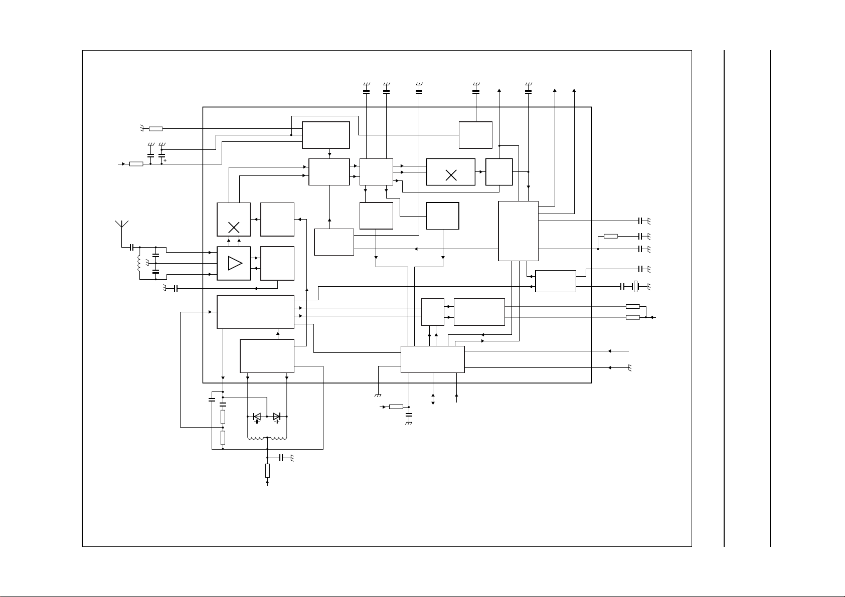
5 BLOCK DIAGRAM
Philips Semiconductors Product specification
Low-power FM stereo radio for
handheld applications
V
CCA
FM antenna
4.7 Ω
100 pF
L1
22 nF
47 nF
LIMDEC2
I
R1
22 µF
27 pF
47 pF
4.7 nF
gain
AGND
V
CCA
RFI1
RFGND
RFI2
TAGC
LOOPSW
10 nF
25
26
27
I/Q-MIXER
1st FM
28
29
30
31
32
TUNING SYSTEM
12
CPOUT VCOTANK2 V
39 nF
10 kΩ
100 kΩ
AGC
VCO
VCOTANK1
D1L3D2
÷2
N1
L2
GAIN
STABILIZATION
RESONANCE
AMPLIFIER
IF CENTRE
FREQUENCY
ADJUST
programmable divider output
reference frequency divider output
34
CC(VCO)
47 nF
LIMDEC1 TIFC
24 23 22 21 20
LIMITER
LEVEL
ADC
5678
DGND CLOCK
12 Ω
V
CCD
47 nF
DEMODULATOR
COUNTER
I
ref
MUX
I2C-BUS
CCD
22 nF
IF
TEA5768HL
PROGRAMMABLE
DATAV
33 nF
V
ref
POWER
SUPPLY
SOFTWARE
PORT
pilot
mono
MPXO TMUTE
SOFT
MUTE
MPX
DECODER
33 nF
V
AFR
19 18 17
SDS
CRYSTAL
OSCILLATOR
mhc275
V
AFL
16
15
14
13
12
11
10
PILFIL
PHASEFIL
XTAL2
XTAL1
SWPORT2
SWPORT1
BUSENABLE
BUSMODE
9
33 kΩ
1 nF
22 nF
22 nF
(1)
C
comp
(1)
C
32.768 kHz
pull
10 kΩ
10 kΩ
or
13 MHz
V
CCA
The component list is given Chapter 14.
(1) C
comp
and C
data depends on crystal specification.
pull
47 Ω
22 nF
V
CC(VCO)
TEA5768HL
Fig.1 Block diagram.

Philips Semiconductors Product specification
Low-power FM stereo radio for
handheld applications
6 PINNING
SYMBOL PIN DESCRIPTION
CPOUT 1 charge pump output of synthesizer PLL
VCOTANK1 2 voltage controlled oscillator tuned circuit output 1
VCOTANK2 3 voltage controlled oscillator tuned circuit output 2
V
CC(VCO)
DGND 5 digital ground
V
CCD
DATA 7 bus data line input/output
CLOCK 8 bus clock line input
BUSMODE 9 bus mode select input
BUSENABLE 10 bus enable input
SWPORT1 11 software programmable port 1
SWPORT2 12 software programmable port 2
XTAL1 13 crystal oscillator input 1
XTAL2 14 crystal oscillator input 2
PHASEFIL 15 phase detector loop filter
PILFIL 16 pilot detector low-pass filter
V
AFL
V
AFR
TMUTE 19 time constant for soft mute
MPXO 20 FM demodulator MPX signal output
V
ref
TIFC 22 time constant for IF centre adjust
LIMDEC1 23 decoupling IF limiter 1
LIMDEC2 24 decoupling IF limiter 2
I
gain
AGND 26 analog ground
V
CCA
RFI1 28 RF input 1
RFGND 29 RF ground
RFI2 30 RF input 2
TAGC 31 time constant RF AGC
LOOPSW 32 switch output of synthesizer PLL loop filter
4 voltage controlled oscillator supply voltage
6 digital supply voltage
17 left audio frequency output voltage
18 right audio frequency output voltage
21 reference voltage
25 gain control current for IF filter
27 analog supply voltage
TEA5768HL
2004 Sep 13 6

Philips Semiconductors Product specification
Low-power FM stereo radio for
handheld applications
CPOUT LIMDEC2
VCOTANK1 LIMDEC1
VCOTANK2 TIFC
V
CC(VCO)
CLOCK V
1
2
3
4
5
DGND MPXO
6
V
CCD
7
DATA V
8
CCA
32313029282726
TEA5768HL
9
10111213141516
XTAL1 RFI1
XTAL2 V
SWPORT1 RFI2
BUSENABLE TAGC
SWPORT2 RFGND
BUSMODE LOOPSW
25
PILFIL I
PHASEFIL AGND
gain
24
23
22
21
V
ref
20
19
TMUTE
18
AFR
17
AFL
001aab494
TEA5768HL
Fig.2 Pin configuration.
7 FUNCTIONAL DESCRIPTION
7.1 Low-noise RF amplifier
The LNA input impedance together with the LC RF input
circuit defines an FM band filter. The gain of the LNA is
controlled by the RF AGC circuit.
7.2 FM mixer
The FM quadrature mixer converts the FM RF
(76 MHz to 108 MHz) to an IF of 225 kHz.
7.3 VCO
The varactor tuned LC VCO provides the Local Oscillator
(LO) signal for the FM quadrature mixer. The VCO
frequency range is 150 MHz to 217 MHz.
7.4 Crystal oscillator
The crystal oscillator can operate with a 32.768 kHz clock
crystal or a 13 MHz crystal. The temperature drift of
standard 32.768 kHz clock crystals limits the operational
temperature range from −10 °C to +60 °C.
The PLL synthesizer can be clocked externally with a
32.768 kHz, a 6.5 MHz or a 13 MHz signal via pin XTAL2.
The crystal oscillator generates the reference frequency
for:
• The reference frequency divider for the synthesizer PLL
• The timing for the IF counter
• The free-running frequency adjustment of the stereo
decoder VCO
• The centre frequency adjustment of the IF filters.
7.5 PLL tuning system
The PLL synthesizer tuning system is suitable to operate
with a 32.768 kHz or a 13 MHz reference frequency
generated by the crystaloscillator or appliedto the IC from
an external source. The synthesizer can also be clocked
via pin XTAL2 at 6.5 MHz. The PLL tuning system can
perform an autonomous search tuning function.
7.6 RF AGC
The RF AGC prevents overloading and limits the amount
of intermodulation products created by strong adjacent
channels.
2004 Sep 13 7

Philips Semiconductors Product specification
Low-power FM stereo radio for
handheld applications
7.7 IF filter
Fully integrated IF filter.
7.8 FM demodulator
The FM quadrature demodulator has an integrated
resonator to perform the phase shift of the IF signal.
7.9 Level voltage generator and analog-to-digital converter
TheFM IF analog level voltage isconvertedto4 bits digital
data and output via the I2C-bus.
7.10 IF counter
The IF counter outputs a 7-bit count result via the I2C-bus.
7.11 Soft mute
The low-pass filtered level voltage drives the soft mute
attenuator at low RF input levels. The soft mute function
can be switched off via the I2C-bus.
7.12 MPX decoder
The PLL stereo decoder is adjustment-free. The stereo
decoder can be switched to mono via the I2C-bus.
TEA5768HL
2
8I
C-BUS AND BUS-CONTROLLED FUNCTIONS
2
8.1 I
InformationabouttheI2C-buscanbefoundinthebrochure
“The I2C-bus and how to use it”
9398 393 40011).
The standard I2C-bus specification is expanded by the
following definitions.
IC address C0: 1100000.
Structure of the I2C-bus logic: slave transceiver.
Subaddresses are not used.
The maximum LOW-level input and the minimum
HIGH-level input are specified to 0.2V
respectively.
The pin BUSMODE must be connected to ground.
Before any READ or WRITE operation the pin
BUSENABLE has to be HIGH for at least 10 µs.
Note: The bus operates at a maximum clock frequency of
400 kHz. It is not allowed to connect the IC to a bus
operating at a higher clock rate.
8.1.1 DATA TRANSFER
C-bus specification
(order number
and 0.45V
CCD
CCD
7.13 Signal dependent mono to stereo blend
With a decreasing RF input level the MPX decoder blends
from stereo to mono to limit the output noise. The
continuousmono to stereo blendcan also be programmed
viathe I2C-busto an RF level depending switchedmono to
stereo transition. Stereo Noise Cancelling (SNC) can be
switched off via the I2C-bus.
7.14 Signal dependent AF response
Theaudio bandwidth will bereduced with a decreasingRF
input level. This function can be switched off via the
I2C-bus.
7.15 Software programmable ports
Two software programmable ports(open-collector) can be
addressed via the I2C-bus.
The port 1 (pin SWPORT1) function can be changed with
write data byte 4 bit 0 (see Table 13). Pin SWPORT1 is
then output for the ready flag of read byte 1.
Datasequence:address,byte 1,byte 2,byte 3, byte 4 and
byte 5 (the data transfer has to be in this order). The
LSB = 0of the address indicates a WRITEoperationto the
TEA5768HL.
Bit 7 of each byte is considered as the MSB and has to be
transferred as the first bit of the byte.
The data becomes valid bitwise at the appropriate falling
edge of the clock. A STOP condition after any byte can
shorten transmission times.
When writing to the transceiver by using the STOP
condition before completion of the whole transfer:
• The remaining bytes will contain the old information
• If thetransfer of a byte isnot completed, the newbitswill
be used, but a new tuning cycle will not be started.
The IC can be switched into a low current standby mode
with the standby bit; the bus is then still active. The
standby current can be reduced by deactivating the bus
interface (pin BUSENABLE LOW). If the bus interface is
deactivated (pin BUSENABLE LOW) without the standby
mode being programmed, the IC maintains normal
operation, but is isolated from the bus lines.
2004 Sep 13 8

Philips Semiconductors Product specification
Low-power FM stereo radio for
handheld applications
The software programmable output (SWPORT1) can be
programmed to operate as a tuning indicator output.
As long as the IC has not completed a tuning action,
pin SWPORT1 remains LOW. The pin becomes HIGH,
when a preset or search tuning is completed or when a
band limit is reached.
The reference frequency divider of the synthesizer PLL is
changed when the MSB in byte 5 is set to logic 1. The
tuning system can then be clocked via pin XTAL2 at
6.5 MHz.
2
8.2 I
Table 1 Write mode
Notes
1. S = START condition.
2. A = acknowledge.
3. P = STOP condition.
C-bus protocol
(1)
S
address (write) A
TEA5768HL
8.1.2 POWER-ON RESET
At Power-on reset the mute is set, all other bits are set to
LOW. To initialize the IC all bytes have to be transferred.
(2)
data byte(s) A
(2)
(3)
P
Table 2 Read mode
(1)
S
address (read) A
(2)
data byte 1
Notes
1. S = START condition.
2. A = acknowledge.
Table 3 IC address byte
IC ADDRESS MODE
1100000R/W
Note
1. Read or write mode:
a) 0 = write operation to the TEA5768HL
b) 1 = read operation from the TEA5768HL.
(1)
2004 Sep 13 9
Philips Semiconductors Product specification
Low-power FM stereo radio for
TEA5768HL
handheld applications
8.3 Writing data
Table 4 Write mode
DATA BYTE 1 DATA BYTE 2 DATA BYTE 3 DATA BYTE 4 DATA BYTE 5
Table 5 Format of 1st data byte
BIT 7 (MSB) BIT 6 BIT 5 BIT 4 BIT 3 BIT 2 BIT 1 BIT 0 (LSB)
MUTE SM PLL13 PLL12 PLL11 PLL10 PLL9 PLL8
Table 6 Description of 1st data byte bits
BIT SYMBOL DESCRIPTION
7 MUTE if MUTE = 1 then L and R audio are muted; if MUTE = 0 then L and R audio are not
muted
6SMSearch Mode: if SM = 1 then in search mode; if SM = 0 then not in search mode
5 to 0 PLL[13:8] setting of synthesizer programmable counter for search or preset
Table 7 Format of 2nd data byte
BIT 7 (MSB) BIT 6 BIT 5 BIT 4 BIT 3 BIT 2 BIT 1 BIT 0 (LSB)
PLL7 PLL6 PLL5 PLL4 PLL3 PLL2 PLL1 PLL0
Table 8 Description of 2nd data byte bits
BIT SYMBOL DESCRIPTION
7 to 0 PLL[7:0] setting of synthesizer programmable counter for search or preset
Table 9 Format of 3rd data byte
BIT 7 (MSB) BIT 6 BIT 5 BIT 4 BIT 3 BIT 2 BIT 1 BIT 0 (LSB)
SUD SSL1 SSL0 HLSI MS MR ML SWP1
Table 10 Description of 3rd data byte bits
BIT SYMBOL DESCRIPTION
7 SUD Search Up/Down: if SUD = 1 then search up; if SUD = 0 then search down
6 and 5 SSL[1:0] Search Stop Level: see Table 11
4 HLSI HIGH/LOW Side Injection: if HLSI = 1 then HIGH side LO injection; if HLSI = 0 then
LOW side LO injection
3MSMono to Stereo: if MS = 1 then forced mono; if MS = 0 then stereo ON
2MRMute Right: if MR = 1 then the right audio channel is muted and forced mono; if MR = 0
then the right audio channel is not muted
1MLMute Left: if ML = 1 then the left audio channel is muted and forced mono; if ML = 0
then the left audio channel is not muted
0 SWP1 Software programmable port 1: if SWP1 = 1 then port 1 is HIGH; if SWP1 = 0 then
port 1 is LOW
2004 Sep 13 10
Philips Semiconductors Product specification
Low-power FM stereo radio for
TEA5768HL
handheld applications
Table 11 Search stop level setting
SSL1 SSL0 SEARCH STOP LEVEL
0 0 not allowed in search mode
0 1 low; level ADC output= 5
1 0 mid; level ADC output = 7
1 1 high; level ADC output = 10
Table 12 Format of 4th data byte
BIT 7 (MSB) BIT 6 BIT 5 BIT 4 BIT 3 BIT 2 BIT 1 BIT 0 (LSB)
SWP2 STBY BL XTAL SMUTE HCC SNC SI
Table 13 Description of 4th data byte bits
BIT SYMBOL DESCRIPTION
7 SWP2 Software programmable port 2: if SWP2 = 1 then port 2 is HIGH; if SWP2 = 0 then
port 2 is LOW
6 STBY Standby: if STBY = 1 then in standby mode; if STBY = 0 then not in standby mode
5BLBand Limits: if BL = 1 then Japanese FM band; if BL = 0 then US/Europe FM band
4 XTAL if XTAL = 1 then f
3 SMUTE Soft MUTE: if SMUTE = 1 then soft mute is ON; if SMUTE = 0 then soft mute is OFF
2 HCC High Cut Control: if HCC = 1 then high cut control is ON; if HCC = 0 then high cut
control is OFF
1 SNC Stereo Noise Cancelling: if SNC = 1 then stereo noise cancelling is ON; if SNC = 0
then stereo noise cancelling is OFF
0SISearch Indicator: if SI = 1 then pin SWPORT1 is output forthe ready flag; if SI = 0 then
pin SWPORT1 is software programmable port 1
= 32.768 kHz; if XTAL = 0 then f
xtal
= 13 MHz
xtal
Table 14 Format of 5th data byte
BIT 7 (MSB) BIT 6 BIT 5 BIT 4 BIT 3 BIT 2 BIT 1 BIT 0 (LSB)
PLLREF DTC −−−−−−
Table 15 Description of 5th data byte bits
BIT SYMBOL DESCRIPTION
7 PLLREF if PLLREF = 1 then the 6.5 MHz reference frequency for the PLL is enabled;
if PLLREF = 0 then the 6.5 MHz reference frequency for the PLL is disabled
6 DTC if DTC = 1 then the de-emphasis time constant is 75 µs; if DTC = 0 then the
de-emphasis time constant is 50 µs
5to0 − not used; position is don’t care
2004 Sep 13 11
 Loading...