

Philips tea1501, tea1501 n DATASHEETS

INTEGRATED CIRCUITS
DATA SH EET
TEA1501
Greeny; GreenChip
Preliminary specification
File under Integrated Circuits, IC11
1998 Aug 19
Philips Semiconductors Preliminary specification
Greeny; GreenChip TEA1501
FEATURES
• Direct off-line operation (90 to 276 V AC)
• Low external component count
• Integrated high voltage startup current source for a fast
startup within 0.25 s
• Integrated power switch: 650 V, 40 Ω, 0.25 A
• Programmable primary peak current
• Data transfer from isolated secondary side to
non-isolated primary side via the transformer
• On/Off function replaces expensive mains switch by a
functional switch.
Green features
• Low current consumption in Off mode, typical 40 µA
• Efficient burst mode operation, for 0.1 to 3 W output
power.
Protection features
• Cycle-by-cycle current control with programmable
primary peak current
• Over-voltage protection
• Under-voltage lockout
• Over-temperature protection.
GENERAL DESCRIPTION
The TEA1501 (Greeny) is the low power member of the
GreenChip family and is especially designed for standby
switched mode power supply applications. Greeny
incorporates all the necessary functions for an efficient
and low cost power supply for 90 to 276 V AC universal
input. Greeny is a monolithic integrated circuit and is
available in a DIP8 package. The design is made in the
BCD_PowerLogic750 process and includes the high
voltage switching device. Using only 7 functional pins,
Greeny contains extensive control functions to form a
flexible and a reliable power supply with a minimum of
external components. Greeny operates in a flyback
topology (see Fig.1) with a fixed switching frequency,
constant primary peak current control and regulates the
output voltage in burst mode.
Applications include low power supplies and standby
power supplies as used in television, monitor, lighting
electronics and domestic appliances with an output power
from 0.1 to 3 W.
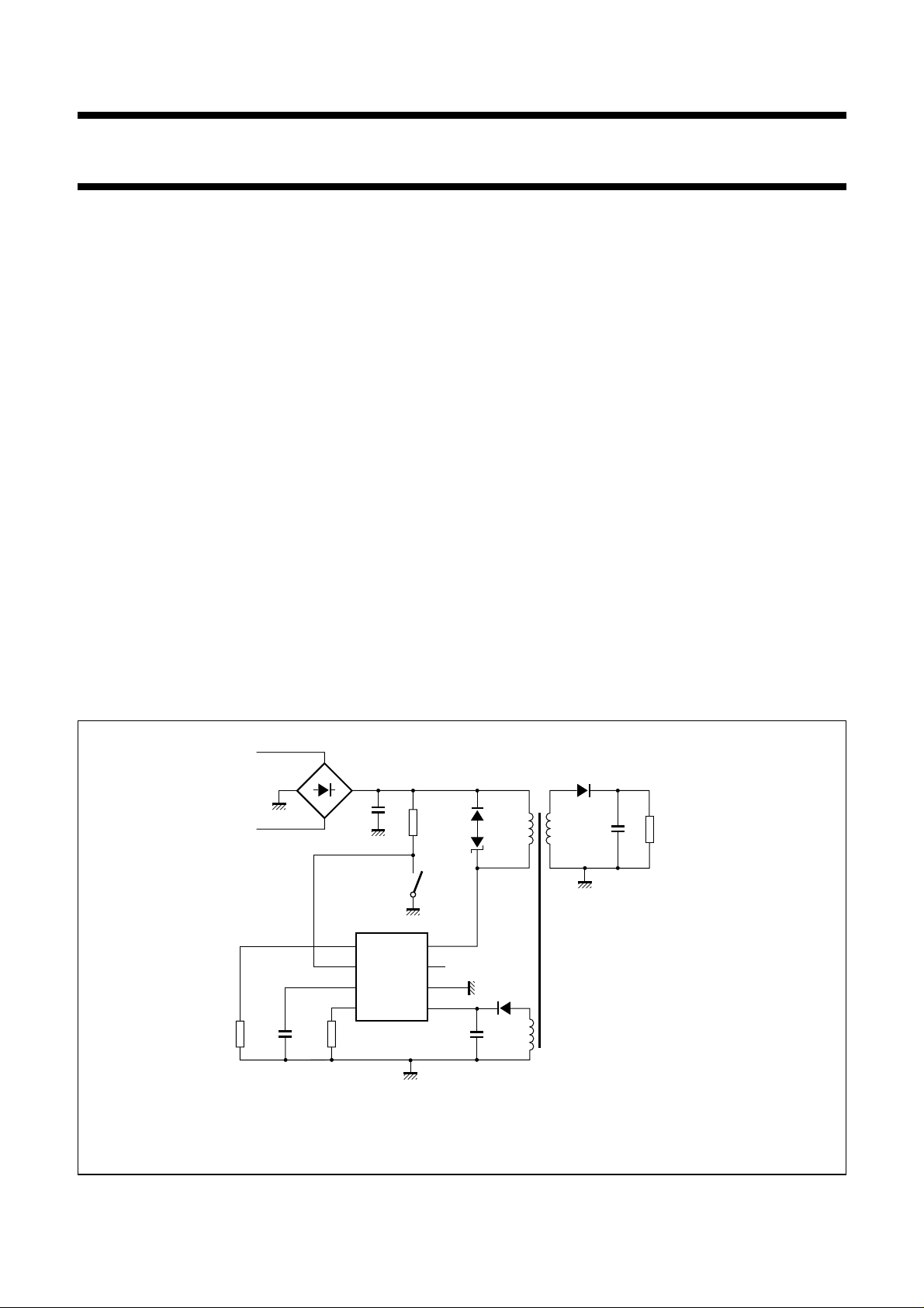
BASIC FLYBACK CONFIGURATION
handbook, full pagewidth
on/off
Src
OOD
TEA1501
Bt
Ref
Src
C
R
Bt
Ref
R
(1) The secondary earthing point is isolated from the primary earthing points.
Fig.1 Basic flyback configuration.
Drn
n.c.
Gnd
Vaux
V
in
n
V
zener
n
n
s
p
a
MGM823
V
out
load
(1)
1998 Aug 19 2

Philips Semiconductors Preliminary specification
Greeny; GreenChip TEA1501
QUICK REFERENCE
SYMBOL PARAMETER CONDITIONS MIN. TYP. MAX. UNIT
V
on/off
V
data(off)
V
data(on)
I
start
I
Drn(off)
V
BD
R
dson
V
detect
ORDERING INFORMATION
on/off level Greeny 0.4 0.7 0.9 V
data off level 20 µA<I
data on level 20 µA<I
startup current, Vaux pin V
drain current in Off mode V
breakdown voltage I
=8V, V
Vaux
< 0.4 V − 40 100 µA
OOD
Drn(off)
on resistance Tj=25°C, I
< 100 µA 0.9 1.3 1.6 V
OOD
< 100 µA 3.5 4.0 4.5 V
OOD
> 0.9 V −2.4 −1.8 −1.2 mA
OOD
+ 100 µA 650 −−V
=80mA 25 40 55 Ω
Drn
detection level 0.47 0.50 0.53 V
TYPE NUMBER
PACKAGE
NAME DESCRIPTION VERSION
TEA1501 DIP8 plastic dual in-line package; 8 leads (300 mil) SOT97-1
1998 Aug 19 3

Philips Semiconductors Preliminary specification
Greeny; GreenChip TEA1501
BLOCK DIAGRAM
handbook, full pagewidth
Gnd
OOD
Vaux Ref
5
SUPPLY CURRENT
TRACKING
6
MODULATOR
3
Bt
BURST OSCILLATOR
on/off level
2
data offdata on
Vaux MANAGEMENT
REFERENCE BLOCK
TEMPERATURE
PROTECTION
LOGIC
COUNTER
48
startup current source
SWITCH
OSCILLATOR
GATE DRIVER
LEADING EDGE
BLANKING
TEA1501
Drn
power
switch
1
Src
V
detect
MGM820
Fig.2 Block diagram.
PINNING
SYMBOL PIN DESCRIPTION
Src 1 source of the power switch and input
for primary current sensing
OOD 2 on/off input and data transfer output
Bt 3 input for burst capacitor
Ref 4 input for reference resistor
Vaux 5 supply input of the IC and input for
voltage regulation
Gnd 6 ground
n.c. 7 not connected to comply with safety
requirements
Drn 8 drain of the power switch and input
for startup current
1998 Aug 19 4
handbook, halfpage
Src
1
2
TEA1501
3
Bt
4
Ref
MGM821
Fig.3 DIL8 Package.
Drn
8
n.c.OOD
7
Gnd
6
Vaux
5

Philips Semiconductors Preliminary specification
Greeny; GreenChip TEA1501
FUNCTIONAL DESCRIPTION
The TEA1501 contains a high voltage power switch, a high
voltage startup circuit and low voltage control circuitry on
the same IC. Together with a transformer and a few
external components a low power, isolated, flyback
converter can be built. The Greeny system operates in a
burst mode. During each burst period the output voltage is
regulated to a desired voltage level.
System operation
N/OFF
O
The Greeny system can be switched on and off by means
of a low cost, low voltage switch. In the Off mode the
startup current source and power switch are disabled. In
the On mode, Greeny delivers the startup current for the
supply capacitor and after the supply voltage reaches the
startup level Greeny activates the power switch.
S
TARTUP
The startup is realized with a high voltage startup current
source instead of a dissipative bleeder resistor which is
commonly used by low voltage control ICs. When Greeny
is switched on, the startup current source is enabled and
starts charging the Vaux capacitor. The startup current
level is high and accurate (typical 1.8 mA) which results in
a well-defined and short startup time, within 0.25 s. After
the supply voltage reaches the startup level the current
source is switched off and the Vaux capacitor supplies the
chip. Reducing the power dissipation in the current source
to zero after startup is one of the green features of Greeny.
O
PERATION
After startup the flyback converter starts delivering energy
to the secondary and auxiliary winding. The Greeny
system works with fixed switching frequency and fixed
peak current.
As all the windings of the flyback transformer have the
same flux variation, the secondary voltage and the
auxiliary voltage are related via the turns-ratio (n
s/na
).
Therefore, the isolated secondary voltage is controlled by
the non-isolated auxiliary voltage.
The burst mode operates by switching at high frequency
until the Vaux voltage reaches its regulation level of 20 V.
Greeny stops switching until the time period set by the
burst oscillator has expired. At the start of the next burst
period Greeny starts switching at high frequency and
repeats the cycle again.
To guarantee a stable operation in a burst mode controlled
system a Vaux slope compensation circuit is integrated in
Greeny. The Greeny system delivers a constant voltage to
the secondary load until a burst duty cycle of 40%.
D
ATA TRANSFER
The TEA1501 has a data transfer function which makes
communication from the isolated secondary side to the
non-isolated primary side of the transformer possible,
without using an opto-coupler. This communication
function is activated by increasing the secondary load.
With this data transfer function a main power supply can
be switched on and off by the Greeny system.
The power delivered to the secondary and auxiliary
winding is proportional to the number of primary current
pulses per burst period, provided that the converter
operates in discontinuous conduction mode. During each
burst period the number of primary current pulses is
counted. A threshold (N
) of 56 pulses is integrated. The
data
clamp level on the OOD pin is set to data-on level from
data-off level in case the N
threshold is passed. This
data
data-on clamp level can be sensed by the on/off input of a
main supply control IC of the GreenChip family. The
data-on clamp level is maintained until a burst appears
with a number of pulses below the N
threshold.
data
1998 Aug 19 5

Philips Semiconductors Preliminary specification
Greeny; GreenChip TEA1501
Waveforms of Greeny in the Off mode, Startup mode and Operation mode
handbook, full pagewidth
V
Drn
detection
level
V
Src
regulation
V
Vaux
level
V
out
V
Bt
OOD
on/off
level
switch
period
switch on
time
operationstartupoff
burst on
time
burst period
V
Fig.4 Waveforms of Greeny in the Off mode, Startup mode and Operation mode.
MGM828
1998 Aug 19 6
 Loading...